EP2124268B1 - Laminiertes piezoelektrisches element, mit dem laminierten piezoelektrischen element ausgestattete einspritzanordnung und kraftstoffeinspritzsystem - Google Patents
Laminiertes piezoelektrisches element, mit dem laminierten piezoelektrischen element ausgestattete einspritzanordnung und kraftstoffeinspritzsystem Download PDFInfo
- Publication number
- EP2124268B1 EP2124268B1 EP07832736.8A EP07832736A EP2124268B1 EP 2124268 B1 EP2124268 B1 EP 2124268B1 EP 07832736 A EP07832736 A EP 07832736A EP 2124268 B1 EP2124268 B1 EP 2124268B1
- Authority
- EP
- European Patent Office
- Prior art keywords
- low rigidity
- layer
- laminated
- piezoelectric element
- portions
- Prior art date
- Legal status (The legal status is an assumption and is not a legal conclusion. Google has not performed a legal analysis and makes no representation as to the accuracy of the status listed.)
- Active
Links
Images







Classifications
-
- F—MECHANICAL ENGINEERING; LIGHTING; HEATING; WEAPONS; BLASTING
- F02—COMBUSTION ENGINES; HOT-GAS OR COMBUSTION-PRODUCT ENGINE PLANTS
- F02M—SUPPLYING COMBUSTION ENGINES IN GENERAL WITH COMBUSTIBLE MIXTURES OR CONSTITUENTS THEREOF
- F02M51/00—Fuel-injection apparatus characterised by being operated electrically
- F02M51/06—Injectors peculiar thereto with means directly operating the valve needle
- F02M51/0603—Injectors peculiar thereto with means directly operating the valve needle using piezoelectric or magnetostrictive operating means
-
- H—ELECTRICITY
- H10—SEMICONDUCTOR DEVICES; ELECTRIC SOLID-STATE DEVICES NOT OTHERWISE PROVIDED FOR
- H10N—ELECTRIC SOLID-STATE DEVICES NOT OTHERWISE PROVIDED FOR
- H10N30/00—Piezoelectric or electrostrictive devices
- H10N30/50—Piezoelectric or electrostrictive devices having a stacked or multilayer structure
- H10N30/508—Piezoelectric or electrostrictive devices having a stacked or multilayer structure adapted for alleviating internal stress, e.g. cracking control layers
-
- H—ELECTRICITY
- H10—SEMICONDUCTOR DEVICES; ELECTRIC SOLID-STATE DEVICES NOT OTHERWISE PROVIDED FOR
- H10N—ELECTRIC SOLID-STATE DEVICES NOT OTHERWISE PROVIDED FOR
- H10N30/00—Piezoelectric or electrostrictive devices
- H10N30/80—Constructional details
- H10N30/87—Electrodes or interconnections, e.g. leads or terminals
- H10N30/875—Further connection or lead arrangements, e.g. flexible wiring boards, terminal pins
-
- F—MECHANICAL ENGINEERING; LIGHTING; HEATING; WEAPONS; BLASTING
- F02—COMBUSTION ENGINES; HOT-GAS OR COMBUSTION-PRODUCT ENGINE PLANTS
- F02M—SUPPLYING COMBUSTION ENGINES IN GENERAL WITH COMBUSTIBLE MIXTURES OR CONSTITUENTS THEREOF
- F02M63/00—Other fuel-injection apparatus having pertinent characteristics not provided for in groups F02M39/00 - F02M57/00 or F02M67/00; Details, component parts, or accessories of fuel-injection apparatus, not provided for in, or of interest apart from, the apparatus of groups F02M39/00 - F02M61/00 or F02M67/00; Combination of fuel pump with other devices, e.g. lubricating oil pump
- F02M63/02—Fuel-injection apparatus having several injectors fed by a common pumping element, or having several pumping elements feeding a common injector; Fuel-injection apparatus having provisions for cutting-out pumps, pumping elements, or injectors; Fuel-injection apparatus having provisions for variably interconnecting pumping elements and injectors alternatively
- F02M63/0225—Fuel-injection apparatus having a common rail feeding several injectors ; Means for varying pressure in common rails; Pumps feeding common rails
Definitions
- the present invention relates to a laminated piezoelectric element applicable for use in, for example, a driving element (piezoelectric actuator), a sensor element and a circuit element.
- the driving element include a fuel jetting device for an automobile engine, a liquid jetting device such as an ink-jet device, a precision positioning device for an optical apparatus or the like, and a vibration preventive device.
- the sensor element include a burning pressure sensor, a knocking sensor, an acceleration sensor, a load sensor, an ultrasonic sensor, a pressure-sensitive sensor and a yaw rate sensor.
- Examples of the circuit element include a piezoelectric gyroscope, a piezoelectric switch, a piezoelectric transformer and a piezoelectric breaker.
- Patent Document 1 an element having a structure in which conductors are connected to a plurality of portions of the external electrode has been proposed. By connecting many conductors to the external electrode, even when a plurality of cracks occur in the external electrode, it is possible to suppress the displacement quantity of the element from being lowered.
- a laminated piezoelectric element including a laminated structure, the structure comprising: a plurality of piezoelectric layers and a plurality of internal electrodes laminated alternately therewith a low rigidity layer that is low in rigidity in comparison with the piezoelectric layers and the internal electrodes and is integrally fired with the piezoelectric layers and the internal electrodes; and a plurality of portions that are divided by the low rigidity lawyer in a laminating direction, which element further includes power supply members of an anode side and a cathode side located on each of the portions, and which low rigidity layer comprises a plurality of metal portions that are mutually separated from one another with a void interposed therebetween.
- the invention provides, in another aspect, a laminated piezoelectric element, including a laminated structure, the structure comprising: a plurality of piezoelectric layers and a plurality of internal electrodes laminated alternately therewith; a low rigidity layer that is low in rigidity in comparison with the piezoelectric layers and the internal electrodes; and a plurality of portions that are divided by the low rigidity layer in a laminating direction, in which the low rigidity layer is a low rigidity metal layer or a low rigidity ceramic layer, power supply members of an anode side and a cathode side are installed on each of the portions, and the low rigidity metal layer comprises a plurality of metal portions that are mutually separated from one another with a void interposed therebetween, and the low rigidity ceramic layer comprises a plurality of ceramic portions that are mutually separated from one another with a void interposed therebetween.
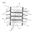
- a laminated piezoelectric element 1 (hereinafter, referred to also as "element 1") of the present background example is provided with a laminated structure 7 in which a plurality of piezoelectric layers 3 and a plurality of internal electrodes 5 are laminated alternately, and external electrodes 9 on an anode side and a cathode side, which are formed on the side faces of the laminated structure 7, and to which the internal electrodes 5 are connected.
- the laminated structure 7 is provided with low rigidity layers 11 each of which is low in rigidity in comparison with the piezoelectric layers 3 and the internal electrodes 5, and is integrally fired with the piezoelectric layers 3 and the internal electrodes 5, and has a plurality of portions divided by the low rigidity layers 11 in a laminating direction.
- At least a pair of current-feeding units 13 (power supply members) electrically connected to the external electrodes 9 on the anode side and the cathode side are disposed on each portion.
- the low rigidity layer 11 refers to a layer having a weak joining force inside the layer and/or a weak joining force to an adjacent layer, in comparison with the piezoelectric layers 3 and the internal electrodes 5. For this reason, cracks tend to occur inside the low rigidity layer 11 and/or on the interface to the adjacent layer.
- the low rigidity layer 11 tends to be damaged upon polarizing or firing in a manufacturing process of a laminated piezoelectric element 1 and during the use of the laminated piezoelectric element 1. For this reason, it is possible to generate a crack at a predetermined position in the laminated structure 7 by using the low rigidity layer 11. If a crack occurs in the piezoelectric layer 3, there is a possibility that an electrical short might develop between the adjacent internal electrodes 5. Moreover, when a crack occurs in the internal electrode 5, a portion is generated to which a voltage is not applied appropriately, resulting in a possibility of a reduction in displacement quantity of the element 1.
- the low rigidity layer 11 it is possible to generate a crack at a predetermined position; in other words, since a position to cause a crack is preliminarily recognized, the current-feeding units 13 to be electrically connected to the external electrodes 9 can be formed on a plurality of portions to be divided in a laminating direction by the low rigidity layers 11 without any loss.
- the respective current-feeding units 13 are placed on the respective portions; therefore, even when cracks occur in a plurality of the low rigidity layers 11 by a long time use of the laminated piezoelectric element 1 to cause damages at a plurality of portions of the external electrodes 9, it is possible to apply a voltage to each of the internal electrodes 5 in a stable manner. Consequently, it becomes possible to prevent a reduction in the displacement quantity of the laminated piezoelectric element 1 due to the occurrence of cracks.
- the rigidities of the low rigidity layer 11, the piezoelectric layer 3 and the internal electrode 5 can be easily compared, for example, by applying a load to the element in a direction perpendicular to a laminating direction. More specifically, it is determined by applying a load to the element 1 in the direction perpendicular to the laminating direction by using a JIS three-point bending test (JIS R 1601) or the like. It is only necessary to determine which portion of the element 1 is damaged upon carrying out the above-mentioned test. The damaged portion corresponds to a portion having the lowest rigidity in the element.
- the laminated piezoelectric element 1 of the present background example is provided with the low rigidity layer 11, a damage preferentially occurs on the low rigidity layer 11 and/or on the interface between the low rigidity layer 11 and the piezoelectric layer 3, rather than on the piezoelectric layer 3 and the internal electrodes 5, when subjected to the JIS three-point bending test. In this manner, it is possible to determine whether the low rigidity layer 11 is present, based upon whether the damaged portion is generated on the piezoelectric layer 3 or the internal electrode 5, or on the low rigidity layer 11 or on the interface between the low rigidity layer 11 and the piezoelectric layer 3.
- the element 1 is processed to form a test piece having a rectangular pillar shape in compliance with the JIS three-point bending test, and the test piece is placed between two fulcrums apart from each other with a predetermined distance, and by applying a load onto a point in the center of the fulcrums, the presence or absence of the low rigidity layer 11 can be determined.
- the low rigidity layer 11 is allowed to have rigidity lower than that of the piezoelectric layer 3 and the internal electrode 5 by using a material having rigidity lower than that of the piezoelectric layer 3 and the internal electrode 5, or by using a structure with many pores formed therein; as will be described later.
- the low rigidity layers are formed by being integrally fired together with the piezoelectric layers and the internal electrodes, it is not necessary to use a laminated structure having a plurality of laminated layers formed with an elastic conductive bonding member being interposed therebetween. For this reason, it is possible to eliminate a process used for joining a plurality of piezoelectric elements to one another by the conductive bonding member. As a result, it is possible to easily manufacture a laminated piezoelectric element.
- the rigidities of the low rigidity layer 11, the piezoelectric layer 3 and the internal electrode 5 can also be evaluated by using the Young's modulus. This is because the low rigidity layer 11 having rigidity smaller than the piezoelectric layer 3 and the internal electrode 5 also has a smaller Young's modulus in comparison with those of the piezoelectric layer 3 and the internal electrode 5. The reason that the Young's modulus of the low rigidity layer 11 is small is because, for example, as will be described later, it has many voids formed therein in comparison with the piezoelectric layer 3 and the internal electrode 5.
- a nano-indentation method may be used as the measuring method of the Young's modulus.
- a "Nano-Indenter II" made by Nano-Instruments Co., Ltd. may be used as the measuring device.
- the piezoelectric layer 3 or the internal electrode 5 is exposed, and the Young's modulus thereof can be measured by using the measuring device.
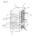
- the laminated piezoelectric element 1 is provided with a laminated structure 7 in which a plurality of piezoelectric layers 3 and a plurality of internal electrodes 5 are laminated alternately, and external electrodes 9 (power supply members) on an anode side and a cathode side, which are formed on the side faces of the laminated structure 7, and to which the internal electrodes 5 are connected.
- the laminated structure 7 is provided with low rigidity layers 11 each of which has low rigidity in comparison with the piezoelectric layers 3 and the internal electrodes 5, and is integrally fired with the piezoelectric layers 3 and the internal electrodes 5.
- the external electrodes 9 are separated from each other to one side and the other side on the side face of the laminated structure 7 in a laminating direction based upon the low rigidity layer 11.
- the low rigidity layer 11 refers to a layer having lower rigidity in comparison with the piezoelectric layer 3 and the internal electrode 5.
- the rigidities of these can be evaluated by using a JIS three-point bending test (JIS R 1601), a test in compliance with the JIS three-point bending test, or a measuring process of the Young's modulus.
- the low rigidity layer 11 also refers to a layer having a weak joining force inside the layer and/or a weak joining force to an adjacent layer, in comparison with the piezoelectric layers 3 and the internal electrodes 5. For this reason, cracks easily occur inside the low rigidity layer 11 and/or on the interface to the adjacent layer.
- the external electrodes 9 are separated from each other to one side and the other side on a side face of the laminated structure 7 in the laminating direction based upon the low rigidity layer 11. Since the external electrodes 9 are separated from each other, that is, since a disconnection section having a predetermined shape is preliminarily formed in the external electrodes 9, influences to the external electrode 9 from cracks caused in the low rigidity layer 11 can be reduced. With this arrangement, it becomes possible to reduce the possibility of an occurrence of a crack in an unexpected direction in the external electrode 9.
- the external electrodes 9 are separated from each other to one side and the other side on the side face of the laminated structure 7 in the laminating direction based upon the low rigidity layer 11.
- the gap between the external electrodes 9 is preferably set to 0.1 to 2 times as long as the average thickness of the low rigidity layer 11. By setting the gap to not less than 0.1 times as long, the influences of cracks occurring in the low rigidity layer 11 can be reduced. Moreover, by setting the gap to not more than 2 times as long, predetermined voltages can be applied to the respective internal electrodes 5 in a stable manner.
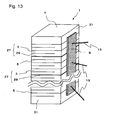
- the laminated piezoelectric element 1 is provided with a laminated structure 7 in which a plurality of piezoelectric layers 3 and a plurality of internal electrodes 5 are laminated alternately, external electrodes 9 on an anode side and a cathode side, which are formed on the side faces of the laminated structure 7, and to which the internal electrodes 5 are connected, and conductive bonding members 15 (power supply members) that are placed on the outer surfaces of the external electrodes 9.
- the laminated structure 7 is provided with low rigidity layers 11 each of which is low in rigidity in comparison with the piezoelectric layers 3 and the internal electrodes 5, and is integrally fired with the piezoelectric layers 3 and the internal electrodes 5.
- the conductive bonding members 15 are separated from each other to one side and the other side on the side face of the laminated structure 7 in a laminating direction based upon the low rigidity layer 11.
- the low rigidity layer 11 refers to a layer having lower rigidity in comparison with the piezoelectric layer 3 and the internal electrode 5 in the same manner as in the first laminated piezoelectric element 1, and the rigidities thereof can be evaluated by a JIS three-point bending test (JIS R 1601), a test in compliance with the JIS three-point bending test, or a measuring process of the Young's modulus.
- JIS R 1601 JIS three-point bending test
- a test in compliance with the JIS three-point bending test or a measuring process of the Young's modulus.
- the low rigidity layer 11 is a layer having a weak joining force inside the layer and/or a weak joining force to an adjacent layer, in comparison with the piezoelectric layers 3 and the internal electrodes 5, cracks easily occur inside the low rigidity layer 11 and/or on the interface to the adjacent layer.
- the conductive bonding members 15 are separated from each other to one side and the other side on the side face of the laminated structure 7 in the laminating direction based upon the low rigidity layer 11. Since the conductive bonding members 15 are separated from each other, that is, since a disconnection section having a predetermined shape is preliminarily formed in the conductive bonding members 15, even upon occurrence of a crack in the low rigidity layer 11, it becomes possible to reduce the possibility of an occurrence of a crack in an unexpected direction in the conductive bonding members 15.
- the conductive bonding members 15 are used for joining the external electrodes 9 to the current-feeding units 13.
- the conductive bonding members 15 are formed on the outer surface of each external electrode 9 in a layer state. This arrangement is made so as to simplify the process for forming the conductive bonding members 15 on the side face of the laminated structure 7 and so as to positively join the external electrode 9 and the current-feeding unit 13 to each other.
- each of the conductive bonding members 15 is formed in the layer state in this manner, the above-mentioned separated structure of the conductive bonding members 15 functions more effectively.
- the thickness of the conductive bonding members 15 is preferably set to 10 ⁇ m to 200 ⁇ m.
- the thickness of 10 ⁇ m or more makes it possible to more positively apply predetermined voltages to the respective internal electrodes 5.
- the thickness of 200 ⁇ m or less makes the conductive bonding members less susceptible to cracks even upon application of a stress caused by repetitive driving operations of the laminated piezoelectric element 1.
- the conductive bonding members 15 are separated from each other to one side and the other side on the side face of the laminated structure 7 in the laminating direction based upon the low rigidity layer 11.
- the gap between the conductive bonding members 15 is preferably set to 0.1 to 3 times as long as the average thickness of the low rigidity layer 11. By setting the gap to not less than 0.1 times as long, the influences of cracks occurring in the low rigidity layer 11 can be reduced. Moreover, by setting the gap to not more than 3 times as long, predetermined voltages can be applied to the respective internal electrodes 5 in a stable manner.
- any material may be used as the conductive bonding member 15 as long as it electrically connects each of the external electrodes 9 on the anode side and the cathode side to the current-feeding units 13. Therefore, specific materials for the conductive bonding member 15 include solder, wax material and conductive resins. In particular, from the viewpoint of durability of a joined portion between the external electrodes 9 and the current-feeding units, solder using an alloy of lead, tin and silver is preferably used.
- the laminated piezoelectric element 1 is preferably designed so that, the external electrodes 9 are separated from each other to one side and the other side on the side face of a laminated structure 7 in the laminating direction based upon the low rigidity layer 11.
- the laminated piezoelectric element 1 is superior in durability, and is continuously operable for a long period of time in a stable manner, even under high electric field and high pressure.
- the piezoelectric layers 3 are preferably made adjacent to each low rigidity layer 11 on both of the sides in its laminating direction. In the case where the piezoelectric layers 3 are made adjacent to the low rigidity layer 11 on both of the sides in the laminating direction, since the low rigidity layer 11 is sandwiched by the piezoelectric members having a high insulating property, it is possible to effectively prevent an electrical short from occurring through a crack generated in the low rigidity layer 11.
- the piezoelectric layers 3 are made adjacent to the low rigidity layer 11 on both of the sides in the laminating direction, even upon occurrence of a crack in the low rigidity layer 11, it becomes possible to reduce the possibility of the internal electrode 5 adjacent to the low rigidity layer 11 in the laminating direction exposing to the crack face. Consequently, it is possible to prevent an electrical short from occurring through a crack generated in a gap between the low rigidity layer 11 and the internal electrode 5 adjacent thereto in the laminating direction and/or a gap between the internal electrode 5 and the external electrode 9.
- any material may be used as long as it has a low rigidity in comparison with the piezoelectric layer 3 and the internal electrodes 5 and it can be integrally fired together with the piezoelectric layer 3 and the internal electrodes 5.
- Specific examples thereof include metal of a simple substance, such as Cu and Ni, and an alloy, such as a silver-platinum alloy and a silver-palladium alloy.
- a silver-palladium alloy is preferably used as its main component.
- the low rigidity layer 11 may be formed by using a metal component as its main component, as described above, or may be made from ceramics or the like.
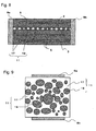
- voids 17 are formed in a low rigidity layer 11, and the low rigidity layer 11 has a void ratio higher than those of the internal electrode 5 and the piezoelectric layer 3. For this reason, the layer is further low in its rigidity in comparison with the piezoelectric layer 3 and the internal electrodes 5. With this arrangement, sites where cracks occur can be more positively concentrated on the low rigidity layer 11 so that the possibility of cracks occurring in the internal electrodes 5 and piezoelectric layers 3 can be reduced.
- the low rigidity layer 11 is provided with a plurality of metal portions 19 that are separated from one another.
- the composition of the low rigidity layer 11 provided with the metal portions 19 can be measured, for example, in the following manner. That is, first, the laminated structure 7 is cut so that the metal portions 19 of the low rigidity layer 11 are exposed. Then, one portion of the low rigidity layer 11 is sampled. Next, by carrying out a chemical analysis such as an ICP (Inductive Coupling Plasma) light emission analysis or the like, the composition of the low rigidity layer 11 can be measured. Alternatively, the cut face of the laminated piezoelectric element 1 may be analyzed and measured by using an EPMA (Electron Probe Micro Analysis) method.
- ICP Inductive Coupling Plasma
- EPMA Electrode Micro Analysis
- the low rigidity layer 11 can be observed under an SEM (Scanningtype Electron Microscope) or under a metal microscope. Moreover, the low rigidity layer 11 can be analyzed by the EPMA method.
- the low rigidity layer 11 preferably has a structure in which a large number of metal portions 19 having mutually different sizes are placed at random.
- the formation of the low rigidity layer 11 into the above-mentioned structure is in particular effective. This structure makes it possible to reduce the possibility of the stress concentrating locally inside the single low rigidity layer 11, and consequently to disperse the stress over a wider range inside the single low rigidity layer 11.
- the low rigidity layer 11 has a plurality of metal portions 19 that are mutually separated from one another with a void 17 interposed therebetween.
- the low rigidity layer 11 has the plurality of the metal portions 19 that are mutually separated from one another with the void 17 interposed therebetween.
- the void ratio refers to a rate (%) of the area occupied by the voids 17 relative to the cross-sectional area of the laminated structure 7 on a cross section perpendicular to, or in parallel with a laminating direction of the laminated structure 7.
- a laminated structure 7 is subjected to a grinding process by using a known grinding means so that the cross section perpendicular to the laminating direction is exposed. More specifically, the grinding process is carried out by using, for example, a bench grinding machine KEMET-V-300 made by Kemet Japan Co., Ltd. as the grinding device, with diamond paste being applied thereto.
- the cross section, thus exposed by the grinding process is observed by using, for example, a scanning electron microscope (SEM), an optical microscope, a metal microscope, or the like so that a cross-sectional image is obtained.
- SEM scanning electron microscope
- the void ratios of the internal electrodes 5 and the low rigidity layer 11 can be measured by image-processing the cross-sectional image.
- void portions are painted into black solid portions, while the other portions except for the void portions are painted into white solid portions. Then, the ratio of the black portions, that is, (the area of black portions) / (the area of black portions + the area of white portions), is found, and this is indicated by percentage so that the void ratio can be calculated. Moreover, in the case where the cross-sectional image is provided as a colored image, the image is converted into gray scales so as to be divided into black portions and white portions.
- the binarizing process may be carried out by setting the threshold value of the border visually or by the use of image processing software.
- the void ratio of the low rigidity layer 11 is preferably set to 10% to 95%. In the case of the void ratio of 10% or more, it is possible to effectively suppress cracks occurred in the low rigidity layer 11 from developing toward the piezoelectric layer 3 and/or the internal electrodes 5. Moreover, in the case of 95% or less, it is possible to maintain the outer shape of the laminated piezoelectric element 1 in a stable manner.
- the low rigidity layer 11 is preferably provided with a plurality of ceramic portions 21 that are separated from one another. This arrangement is made so that, since the ceramic portions 21 themselves are successively damaged, a stress, caused by the displacement of the piezoelectric layer 3, can be dispersed over a wide range. Thus, it is possible to provide a highly reliable laminated piezoelectric element 1 with high durability.
- a perovskite-type oxide such as lead-zirconate- titanate (PbZrO 3 -PbTiO 3 )
- PbZrO 3 -PbTiO 3 lead-zirconate- titanate
- the component of the ceramic portions 21 can be analyzed and measured by using an analyzing method, such as an EPMA method, as described earlier.
- the low rigidity layer 11 preferably has a structure in which a large number of ceramic portions 21 having mutually different sizes are placed at random.
- the formation of the low rigidity layer 11 into the above-mentioned structure is in particular effective. This structure makes it possible to reduce the possibility of the stress concentrating locally a part of the low rigidity layer 11, and consequently to disperse the stress over a wider range therein.
- the low rigidity layer 11 is preferably provided with a plurality of ceramic portions 21 that are separated from one another with a void 17 interposed therebetween. This arrangement is made so that, since the ceramic portions 21 themselves are more easily damaged, a stress caused by the displacement of the piezoelectric layer 3, can be dispersed over a wide range.
- the void ratio of the low rigidity layer 11 is preferably set to 30% to 90%.
- the stress dispersing effect by the low rigidity layer 11 is enhanced so that it is possible to provide a highly reliable laminated piezoelectric element 1.
- the void ratio is more preferably set to 50% or more.
- the low rigidity layer 11 is mainly formed by pillar-shaped ceramic portions 21.
- the piezoelectric layers 3 made in contact with the low rigidity layer 11 are supported by these ceramic portions 21.
- the void ratio refers to a rate (%) of the area occupied by the voids 17 relative to the cross-sectional area of the low rigidity layer 11 on a cross section perpendicular to, or in parallel with a laminating direction of the laminated structure 7.
- the method described earlier may be used as a method for measuring the void ratio.
- the low rigidity layer 11 is provided with a plurality of metal portions 19 and a plurality of ceramic portions 21 that are mutually separated from one another so that a laminated piezoelectric element 1 that is superior in durability can be achieved.
- the low rigidity layer 11 is provided with the metal portions 19 and the ceramic portions 21, and each of the metal portions 19 and each of the ceramic portions 21 are preferably designed to have portions that are made in contact with each other.
- the stress alleviating effect is exerted more greatly.
- the metal portions 19 and the ceramic portions 21 have respective features in their stress-alleviating functions and effects.
- the respective features in their stress-alleviating effects are obtained, since these portions are allowed to function integrally.
- the portions 19 and the ceramic portions 21 are preferably set to virtually the same ratio.
- the ratio refers to a ratio between the total area of the metal portions 19 and the total area of the ceramic portions 21 on a cross section perpendicular to, or in parallel with the laminating direction of the laminated structure 7.
- each ceramic portion 21 is preferably formed by a piezoelectric member.
- a higher stress alleviating effect is exerted. This is because, by placing the piezoelectric members so as to be separated from each other, the ceramic portions 21 serving as the piezoelectric members are allowed to have a higher degree of freedom. In the case where the degree of freedom in the ceramic portions 21 becomes higher, upon occurrence of a stress in each ceramic portion 21, ion positions inside the piezoelectric crystal are moved so that the crystal structure is easily deformed in response to the direction of the stress. Thus, it becomes possible to obtain a high stress-alleviating effect.
- the thickness of the low rigidity layer 11 is preferably set to 1 to 20 ⁇ m. In the case of the thickness of 1 ⁇ m or more, since the low rigidity layer 11 is easily deformed, the stress can be dispersed over a wide range. Moreover, in the case of the thickness of 20 ⁇ m or less, it is possible to stabilize a position where a rupture occurs in the low rigidity layer 11.
- the laminated structure 7 is designed to have a plurality of low rigidity layers 11 in the laminating direction. More specifically, a low rigidity layer 11 is preferably disposed for every 5 to 300 piezoelectric layers 3. By disposing a low rigidity layer 11 for every 5 or more piezoelectric layers 3, the binding force of the piezoelectric layers 3 is improved so that the joining strength to the piezoelectric layers 3 can be improved. Moreover, by disposing a low rigidity layer 11 for every not less than 300 piezoelectric layers 3, the binding force of the piezoelectric layers 3 can be sufficiently dispersed.
- a plurality of low rigidity layers 11 are installed, and these are preferably disposed regularly in the laminating direction. By regularly disposing these, the entire binding force of the laminated structure 7 is dispersed, and it is possible to suppress a reduction in the amount of change in piezoelectric displacement even during a driving operation under a low temperature for a long period of time, and consequently to provide a stable driving operation for a long period of time.
- the gap between the respective low rigidity layers 11 is formed into a fixed distance so that it is possible to provide a simple structure that is easily manufactured, and also to prevent cracks from occurring on portions other than the low rigidity layers 11.
- the low rigidity layers 11 may be disposed with fixed intervals in the laminating direction of the laminated structure 7, or may be disposed with gradually widening intervals from the center in the laminating direction toward the two end faces, as shown in Fig. 11 .
- this layout of the low rigidity layers 11 makes it possible to suppress concentration of the stress, and consequently to disperse the stress. With this arrangement, it is possible to suppress a strain from occurring in the laminated structure 7 upon application of a voltage.
- another structure may be used in which, in the vicinity of the center of the laminated structure 7 on which the stress is concentrated, a plurality of the low rigidity layers 11 are disposed with fixed intervals, and on the two ends of this portion in which the low rigidity layers 11 are disposed with fixed intervals, the low rigidity layers 11 are disposed with gradually increasing intervals.
- the stress is prevented from being concentrated, while being dispersed, and it is possible to manufacture a laminated piezoelectric element 1 having a large displacement quantity.
- a laminated piezoelectric element 1 is provided with a laminated structure 7 in which a plurality of piezoelectric layers 3 and a plurality of metal layers 23 are alternately laminated and external electrodes 9 on an anode side and a cathode side, which are formed on the side faces of the laminated structure 7.
- Each metal layer 23 is provided with internal electrodes 5 that are connected to the external electrodes 9 on the anode side and the cathode side, and low rigidity metal layers 25 having low rigidity in comparison with the piezoelectric layers 3 and the internal electrodes 5.
- the laminated structure 7 has a plurality of portions that are divided by the low rigidity metal layers 25 in a laminating direction. At least a pair of current-feeding units 13 (power supply members) electrically connected to the external electrodes 9 on the anode side and the cathode side are disposed on each portion.
- the low rigidity metal layer 25 refers to a layer that is low in rigidity in comparison with the piezoelectric layers 3 and the internal electrodes 5, and has a weak joining force inside the layer and/or a weak joining force to an adjacent layer. For this reason, cracks tend to occur inside the low rigidity metal layer 25 and/or on the interface to the adjacent layer.
- each of the low rigidity metal layers 25 tends to be damaged upon polarizing or firing in a manufacturing process of a laminated piezoelectric element 1 and during the use of the laminated piezoelectric element 1.
- the above-mentioned low rigidity metal layers make it possible to reduce the possibility of occurrence of cracks in the internal electrode 5 and the piezoelectric layer 3. Consequently, it becomes possible to provide a highly reliable laminated piezoelectric element 1 that can be driven in a stable manner.
- the current-feeding units 13 to be electrically connected to the external electrodes 9 can be formed on a plurality of portions to be divided in a laminating direction by the low rigidity metal layers 25 without any loss.
- the rigidities of the low rigidity metal layer 25, the piezoelectric layer 3 and the internal electrode 5 can be evaluated by using a JIS three-point bending test (JIS R 1601), a test in compliance with the JIS three-point bending test, or measurements of the Young's modulus.
- JIS R 1601 JIS three-point bending test
- a test in compliance with the JIS three-point bending test or measurements of the Young's modulus.
- the laminated piezoelectric element 1 of the present embodiment is provided with the low rigidity metal layers 25, a damage preferentially occurs on the low rigidity metal layer 25 and/or on the interface between the low rigidity metal layer 25 and the piezoelectric layer 3, rather than on the piezoelectric layer 3 and the internal electrodes 5, when subjected to the JIS three-point bending test. In this manner, it is possible to determine whether the low rigidity metal layer 25 is present, based upon whether the ruptured portion is generated on the piezoelectric layer 3 or the internal electrode 5, or on the low rigidity metal layer 25 or on the interface between the low rigidity metal layer 25 and the piezoelectric layer 3.
- the low rigidity metal layer 25 is allowed to have rigidity lower than that of the piezoelectric layer 3 and the internal electrode 5 by using a material having rigidity lower than that of the piezoelectric layer 3 and the internal electrode 5, or by using a structure with many pores 17 formed therein, as will be described later.
- the external electrodes 9 are preferably separated from each other to one side and the other side on the side faces of the laminated structure 7 in the laminating direction based upon the low rigidity metal layer 25. Since the external electrodes 9 are separated from each other to one side and the other side on the side faces of the laminated structure 7 in the laminating direction based upon the low rigidity metal layer 25, it becomes possible to prevent a crack from occurring in an unexpected direction in the external electrodes 9.
- conductive bonding members 15, which are separated from each other to one side and the other side in the laminating direction based upon the low rigidity metal layer 25, are preferably disposed on the outer surface of the external electrodes 9. Since the conductive bonding members 15 are disposed in this manner, it is possible to electrically connect the external electrodes 9 to the current-feeding units 13 stably by using a simply process in the same manner as in a third laminated piezoelectric element 1.
- each low rigidity metal layer 25 is provided with a plurality of metal portions 19 that are separated from one another.
- the low rigidity metal layer 25 by forming the low rigidity metal layer 25 in this manner, it becomes possible to reduce the binding force inside the low rigidity metal layer 25 and/or the binding force thereof to an adjacent layer. Thus, the rigidity thereof can be further reduced.
- the composition of the low rigidity metal layer 25 having the metal portions 19 can be analyzed and measured by using an analyzing method, such as an EPMA (Electron Probe Micro Analysis) method.
- an analyzing method such as an EPMA (Electron Probe Micro Analysis) method.
- the low rigidity metal layer 25 for example, metal of a simple substance, such as Cu and Ni, and an alloy, such as a silver-platinum alloy and a silver-palladium alloy, may be used.
- a silver-palladium alloy is preferably used as its main component.
- the low rigidity metal layer 25 preferably has a plurality of metal portions 19 that are mutually separated from one another with a void 17 interposed therebetween.
- the low rigidity metal layer 25 since the low rigidity metal layer 25 has such a structure, it is possible to further reduce the possibility of cracks occurring in the internal electrodes 5 and piezoelectric layer 3.
- the metal portions 19 that are mutually separated from one another with the void 17 interposed therebetween are prepared, it is possible to effectively reduce the possibility of an electrical short occurring through a crack generated in the low rigidity metal layer 25.
- the void ratio refers to a rate (%) of the area occupied by the voids 17 relative to the cross-sectional area of the laminated structure 7 on a cross section perpendicular to, or in parallel with a laminating direction of the laminated structure 7.
- the same method as that of the low rigidity layer 11 may be used as described earlier.
- a laminated piezoelectric element 1 is provided with a laminated structure 7 in which a plurality of ceramic layers 27 and a plurality of internal electrodes 5 are laminated alternately, and external electrodes 9 on an anode side and a cathode side, which are formed on the side faces of the laminated structure 7, and to which the internal electrodes 5 are connected.
- each ceramic layer 27 is provided with a piezoelectric layer 3 and a low rigidity ceramic layer 29 having low rigidity in comparison with the piezoelectric layers 3 and the internal electrodes 5.
- the laminated structure 7 has a plurality of portions divided by the low rigidity ceramic layers 29 in a laminating direction. At least a pair of current-feeding units 13 (power supply members) electrically connected to the external electrodes 9 on the anode side and the cathode side are disposed on each portion.
- each low rigidity ceramic layer 29 refers to a layer that is low in rigidity in comparison with the piezoelectric layer 3 and the internal electrode 5, and has a weak joining force inside the layer and/or a weak joining force to an adjacent layer. For this reason, cracks tend to occur inside the low rigidity ceramic layer 29 and/or on the interface to the adjacent layer.
- each of the low rigidity ceramic layers 29 tends to be damaged upon polarizing or firing in a manufacturing process of a laminated piezoelectric element 1 and during the use of the laminated piezoelectric element 1. For this reason, it becomes possible to reduce the possibility of cracks occurring in the internal electrode 5 and the piezoelectric layer 3. Consequently, it becomes possible to provide a highly reliable laminated piezoelectric element 1 that is operable in a stable manner.
- the current-feeding units 13 to be electrically connected to the external electrodes 9 can be formed on a plurality of portions to be divided in a laminating direction by the low rigidity ceramic layers 29 without any loss.
- the rigidities of the low rigidity ceramic layer 29, the piezoelectric layer 3 and the internal electrode 5 can be evaluated by using a JIS three-point bending test (JIS R 1601), a test in compliance with the JIS three-point bending test, or measurements of the Young's modulus.
- JIS R 1601 JIS three-point bending test
- a test in compliance with the JIS three-point bending test or measurements of the Young's modulus.
- the laminated piezoelectric element 1 of the present background example is provided with the low rigidity ceramic layers 29, a rupture preferentially occurs on the low rigidity ceramic layer 29 or on the interface between the low rigidity ceramic layer 29 and the piezoelectric layer 3, rather than on the piezoelectric layer 3 and the internal electrodes 5, when subjected to the JIS three-point bending test. In this manner, it is possible to determine whether the low rigidity ceramic layer 29 is present, based upon whether the ruptured portion is generated on the piezoelectric layer 3 and the internal electrode 5, or on the low rigidity ceramic layer 29 or on the interface between the low rigidity ceramic layer 29 and the piezoelectric layer 3.
- the low rigidity ceramic layer 29 is allowed to have rigidity lower than that of the piezoelectric layer 3 and the internal electrode 5 by using a material having rigidity lower than that of the piezoelectric layer 3 and the internal electrode 5, or by using a structure with many pores 17 formed therein, as will be described later.
- the external electrodes 9 are preferably separated from each other to one side and the other side on the side faces of the laminated structure 7 in the laminating direction based upon the low rigidity ceramic layer 29. Since the external electrodes 9 are separated from each other to one side and the other side on the side faces of the laminated structure 7 in the laminating direction based upon the low rigidity ceramic layer 29, it becomes possible to prevent a crack from occurring in an unexpected direction in the external electrodes 9.
- conductive bonding members 15, which are separated from each other to one side and the other side in the laminating direction based upon the low rigidity ceramic layer 29, are preferably disposed on the outer surface of the external electrodes 9. Since the conductive bonding members 15 are formed in this manner, it is possible to electrically connect the external electrodes 9 to the current-feeding units 13 stably by using a simply process in the same manner as in the third laminated piezoelectric element 1.
- each low rigidity ceramic layer 29 is preferably provided with a plurality of ceramic portions 21 that are separated from one another.
- the low rigidity ceramic layer 29 by forming the low rigidity ceramic layer 29 in this manner, it becomes possible to reduce the binding force inside the low rigidity ceramic layer 29 and/or the binding force thereof to an adjacent layer. Thus, the rigidity thereof can be further reduced.
- the composition of the low rigidity ceramic layer 29 having the ceramic portions 21 can be analyzed and measured by using an analyzing method, such as an EPMA (Electron Probe Micro Analysis) method.
- an analyzing method such as an EPMA (Electron Probe Micro Analysis) method.
- a perovskite-type oxide such as lead-zirconate-titanate (PbZrO 3 -PbTiO 3 ), can be used as the ceramic portions 21.
- the low rigidity ceramic layer 29 is preferably provided with a plurality of ceramic portions 21 that are separated from one another with a void 17 interposed therebetween.
- the void ratio of the low rigidity ceramic layer 29 is preferably set to 30% to 90%.
- the void ratio refers to a rate (%) of the area occupied by the voids 17 relative to the area of the low rigidity ceramic layer 29 on the cross section perpendicular to, or in parallel with a laminating direction of the laminated structure 7, in the same manner as in the low rigidity layer 11.
- the same method as described earlier may be used.
- each ceramic portion 21 is preferably formed by a piezoelectric member.
- a higher stress alleviating effect is exerted. This is because, by placing the piezoelectric members so as to be separated from each other, the ceramic portions 21 serving as the piezoelectric members are allowed to have a higher degree of freedom. In the case where the degree of freedom in the ceramic portions 21 becomes higher, upon occurrence of a stress in each ceramic portion 21, ion positions inside the piezoelectric crystal are moved so that the crystal structure is easily deformed in response to the direction of the stress. Thus, it becomes possible to obtain a high stress-alleviating effect.
- the thickness of the piezoelectric layer 3 is preferably set to 0.05 mm or more. By setting the thickness of the piezoelectric layer 3 to 0.05 mm or more, it is possible to maintain a high insulating property between the adjacent internal electrodes 5, even upon application of a high voltage to the laminated piezoelectric element 1. With this structure, it becomes possible to obtain a greater displacement quantity. Moreover, the thickness of the piezoelectric layer 3 is preferably set to 0.25 mm or less. By setting the thickness of the piezoelectric layer 3 to 0.25 mm or less, it becomes possible to achieve a small size of the laminated piezoelectric element 1.
- any material may be used as the piezoelectric layer 3 as long as it is a ceramic material having a piezoelectric property.
- a ceramic material having a high piezoelectric strain constant d 33 is preferably used.
- a piezoelectric ceramic material mainly composed of lead titanate-zirconate Pb(Zr, Ti)O 3 or barium titanate BaTiO 3 , may be used.
- each internal electrode 5 is preferably set to 1 to 10 ⁇ m. By setting the thickness of the internal electrode 5 to 1 ⁇ m or more, it becomes possible to apply a predetermined voltage in a stable manner. Moreover, by setting the thickness of the internal electrode 5 to 10 ⁇ m or less, it becomes possible to more positively prevent disconnection in the internal electrode 5.
- a material for the internal electrode 5 for example, metal of a simple substance, such as Cu and Ni, and an alloy, such as a silver-platinum alloy and a silver-palladium alloy, may be used.
- a silver-palladium alloy is preferably used as its main component.
- external electrodes 9 on the anode side and the cathode side are formed.
- internal electrodes 5 or, in some cases, low rigidity layers 11 are electrically connected alternately for every other layer.
- these may be formed either on the opposing side faces or on the adjacent side faces.
- any material may be used as long as it has good conductivity.
- metal of a simple substance such as Cu and Ni, or an alloy thereof may be used.
- silver or an alloy mainly composed of silver is preferably used.
- the current-feeding unit 13 although not particularly limited as long as it has conductivity, for example, metal of a simple substance, such as Cu and Ni, and an alloy, such as a silver- platinum alloy and a silver-palladium alloy, may be used.
- a degreasing process is preferably carried out at a temperature that is higher than Tg temperature of the scattering component.
- silver powder having an average particle size of 2 ⁇ m, glass powder containing silica having an average particle size of 2 ⁇ m, with a softening point of 650°C, and a binder were mixed so that a silver glass conductive paste was prepared.
- This silver glass conductive paste was screen-printed on a portion of each side face of the laminated structure 7 on which external electrodes 9 were to be formed, with a thickness of 30 ⁇ m.
- the laminated structure 7 with the silver glass conductive paste printed on each side face was baked at 700°C for 30 minutes so that a laminated structure 7, provided with external electrodes 9, was manufactured.
- a laminated structure 7 was obtained by using the same method as example 1. Next, resist used for reducing wettability was applied to portions of the side face of the laminated structure 7, located on the side of the low rigidity layer 11. Thereafter, silver powder having an average particle size of 2 ⁇ m and glass powder containing silica having an average particle size of 2 ⁇ m, with a softening point of 650°C, were mixed. Moreover, by adding a binder to this mixture, a silver glass conductive paste was prepared. This silver glass conductive paste was screen-printed on a portion of each side face of the laminated structure 7 on which external electrodes 9 were to be formed, with a thickness of 30 ⁇ m.
Landscapes
- Engineering & Computer Science (AREA)
- Chemical & Material Sciences (AREA)
- Combustion & Propulsion (AREA)
- Mechanical Engineering (AREA)
- General Engineering & Computer Science (AREA)
- Fuel-Injection Apparatus (AREA)
- General Electrical Machinery Utilizing Piezoelectricity, Electrostriction Or Magnetostriction (AREA)
Claims (8)
- Laminiertes piezoelektrisches Element (1), eine laminierte Struktur (7) beinhaltend, wobei die Struktur umfasst:eine Vielzahl von piezoelektrischen Schichten (3) und eine Vielzahl von damit alternierend laminierten internen Elektroden (5);eine Schicht geringer Steifigkeit (11), welche im Vergleich zu den piezoelektrischen Schichten und den internen Elektroden eine geringe Steifigkeit aufweist und integral mit den piezoelektrischen Schichten und den internen Elektroden gebrannt ist; undeine Vielzahl von Abschnitten, die von der Schicht geringer Steifigkeit in einer Laminierrichtung unterteilt werden,wobei das Element weiterhin Stromversorgungsbauteile (9) einer anodischen Seite und einer kathodischen Seite beinhaltet, welche sich an jedem der Abschnitte befinden,dadurch gekennzeichnet, dassSchicht geringer Steifigkeit eine Vielzahl von Metallabschnitten (19) aufweist, welche gegenseitig durch eine dazwischen liegende Lücke (17) voneinander getrennt sind.
- Laminiertes piezoelektrisches Element (1), eine laminierte Struktur (7) beinhaltend, wobei die Struktur umfasst:eine Vielzahl von piezoelektrischen Schichten (3) und eine Vielzahl von damit alternierend laminierten internen Elektroden (5);eine Schicht geringer Steifigkeit (11), welche im Vergleich zu den piezoelektrischen Schichten und den internen Elektroden eine geringe Steifigkeit aufweist; undeine Vielzahl von Abschnitten, die von der Schicht geringer Steifigkeit in einer Laminierrichtung unterteilt werden,wobei die Schicht geringer Steifigkeit eine Metallschicht geringer Steifigkeit oder eine Keramikschicht geringer Steifigkeit ist, Stromversorgungsbauteile (9) einer anodischen Seite und einer kathodischen Seite auf jedem der Abschnitte montiert sind,dadurch gekennzeichnet, dassMetallschicht geringer Steifigkeit eine Vielzahl von Metallabschnitten (19) aufweist, welche gegenseitig durch eine dazwischen liegende Lücke (17) voneinander getrennt sind, und die Keramikschicht geringer Steifigkeit eine Vielzahl von Keramikabschnitten (21) aufweist, welche gegenseitig durch eine dazwischen liegende Lücke (17) voneinander getrennt sind.
- Das laminierte piezoelektrische Element gemäß Anspruch 1 oder 2, weiterhin umfassend externe Elektroden der anodischen Seite und der kathodischen Seite, wobei jede externe Elektrode auf einer Seitenfläche der laminierten Struktur vorgesehen ist und mit den internen Elektroden verbunden ist,
wobei die Stromversorgungsbauteile ein Paar von Stromversorgungseinheiten (13) umfassen, welche elektrisch jeweils mit den externen Elektroden der anodischen Seite und der kathodischen Seite verbunden sind, wobei das Paar von Stromversorgungseinheiten auf jedem der Abschnitte montiert sind. - Das laminierte piezoelektrische Element gemäß Anspruch 1 oder 2, wobei die Stromversorgungsbauteile externe Elektroden sind, welche voneinander zu einer der Seiten und der anderen Seite in einer Laminierrichtung getrennt sind, basierend auf der Position der Schicht geringer Steifigkeit auf einer Seitenfläche der laminierten Struktur.
- Das laminierte piezoelektrische Element gemäß Anspruch 1 oder 2, wobei die Stromversorgungsbauteile leitende Verbindungselemente sind, welche voneinander zu einer der Seiten und der anderen Seite in einer Laminierrichtung getrennt sind, basierend auf der Position der Schicht geringer Steifigkeit auf einer Seitenfläche der laminierten Struktur.
- Das laminierte piezoelektrische Element gemäß einem der vorhergehenden Ansprüche, wobei die laminierte Struktur eine Vielzahl der Schichten geringer Steifigkeit in der Laminierrichtung aufweist.
- Düsenvorrichtung (33), umfassend:das laminierte piezoelektrische Element gemäß einem der vorhergehenden Ansprüche; undeine Düsenöffnung (35),wobei die Vorrichtung eingerichtet ist, eine Flüssigkeit aus der Düsenöffnung zu entladen, wenn das laminierte piezoelektrische Element angesteuert wird.
- Kraftstoffdüsensystem (49), umfassend:ein gemeinsames Verteilerrohr (51), das ausgestaltet ist, einen Hochdruckkraftstoff zu speichern;die Düsenvorrichtung gemäß Anspruch 7, welche ausgestaltet ist, den in dem gemeinsamen Verteilerrohr gespeicherten Kraftstoff zu versprühen;eine Druckpumpe (53), welche ausgestaltet ist, das gemeinsame Verteilerrohr mit Hochdruckkraftstoff zu versorgen; undeine Düsenkontrolleinheit (55), welche ausgestaltet ist, ein Steuersignal an die Düsenvorrichtung auszugeben.
Applications Claiming Priority (2)
| Application Number | Priority Date | Filing Date | Title |
|---|---|---|---|
| JP2006320969 | 2006-11-29 | ||
| PCT/JP2007/073021 WO2008066098A1 (fr) | 2006-11-29 | 2007-11-29 | Elément piézoélectrique laminé, dispositif de projection fourni avec l'élément piézoélectrique laminé et système de projection de carburant |
Publications (3)
| Publication Number | Publication Date |
|---|---|
| EP2124268A1 EP2124268A1 (de) | 2009-11-25 |
| EP2124268A4 EP2124268A4 (de) | 2013-10-23 |
| EP2124268B1 true EP2124268B1 (de) | 2015-04-15 |
Family
ID=39467888
Family Applications (1)
| Application Number | Title | Priority Date | Filing Date |
|---|---|---|---|
| EP07832736.8A Active EP2124268B1 (de) | 2006-11-29 | 2007-11-29 | Laminiertes piezoelektrisches element, mit dem laminierten piezoelektrischen element ausgestattete einspritzanordnung und kraftstoffeinspritzsystem |
Country Status (5)
| Country | Link |
|---|---|
| US (1) | US8049397B2 (de) |
| EP (1) | EP2124268B1 (de) |
| JP (1) | JP5066098B2 (de) |
| CN (2) | CN102290526B (de) |
| WO (1) | WO2008066098A1 (de) |
Families Citing this family (23)
| Publication number | Priority date | Publication date | Assignee | Title |
|---|---|---|---|---|
| EP1942533B1 (de) * | 2005-10-28 | 2013-05-01 | Kyocera Corporation | Geschichtetes piezoelektrisches element und injektionsvorrichtung damit |
| DE102006026644A1 (de) * | 2006-06-08 | 2007-12-13 | Robert Bosch Gmbh | Piezoelektrischer Aktor |
| WO2009038080A1 (ja) * | 2007-09-18 | 2009-03-26 | Kyocera Corporation | 積層型圧電素子、これを備えた噴射装置及び燃料噴射システム |
| JP5334972B2 (ja) * | 2008-06-30 | 2013-11-06 | 京セラ株式会社 | 積層型圧電素子、これを備えた噴射装置および燃料噴射システム |
| JP5339885B2 (ja) * | 2008-12-22 | 2013-11-13 | 京セラ株式会社 | 積層型圧電素子、これを備えた噴射装置および燃料噴射システム |
| DE102009043000A1 (de) * | 2009-05-29 | 2010-12-02 | Epcos Ag | Piezoelektrisches Vielschichtbauelement |
| DE102009034099A1 (de) * | 2009-07-21 | 2011-01-27 | Epcos Ag | Piezoaktor mit elektrischer Kontaktierung |
| DE102010006587A1 (de) | 2010-02-02 | 2011-08-04 | Epcos Ag, 81669 | Piezoelektrisches Bauelement |
| JP2011176187A (ja) * | 2010-02-25 | 2011-09-08 | Kyocera Corp | 積層型圧電素子およびこれを備えた噴射装置ならびに燃料噴射システム |
| CN101840991B (zh) * | 2010-04-30 | 2012-01-25 | 清华大学 | 电致动结构及电致动元件 |
| WO2012011302A1 (ja) * | 2010-07-21 | 2012-01-26 | 京セラ株式会社 | 積層型圧電素子およびこれを備えた噴射装置ならびに燃料噴射システム |
| DE102010042969A1 (de) * | 2010-10-26 | 2012-04-26 | Continental Automotive Gmbh | Piezoelektrisches Bauteil mit Kontaktierung |
| WO2013057940A1 (ja) | 2011-10-19 | 2013-04-25 | パナソニック株式会社 | 電子機器 |
| JP5842635B2 (ja) * | 2012-01-27 | 2016-01-13 | Tdk株式会社 | 積層型圧電素子 |
| JP5905292B2 (ja) * | 2012-02-21 | 2016-04-20 | 日本碍子株式会社 | 圧電素子及び圧電素子の製造方法 |
| US9579691B2 (en) | 2013-05-21 | 2017-02-28 | Mplus Co., Ltd. | Piezoelectric element and electronic component including the same |
| JP5611427B2 (ja) * | 2013-07-31 | 2014-10-22 | 京セラ株式会社 | 積層型圧電素子、これを備えた噴射装置および燃料噴射システム |
| DE102015117203A1 (de) * | 2015-10-08 | 2017-04-13 | Epcos Ag | Drucksensor |
| WO2020170962A1 (ja) * | 2019-02-18 | 2020-08-27 | 株式会社バルカー | 圧電センサーおよび圧電センサーの製造方法 |
| AT523510B1 (de) * | 2020-01-29 | 2021-10-15 | Piezocryst Advanced Sensorics | Strukturiertes, piezoelektrisches Sensorelement |
| KR102825915B1 (ko) * | 2020-09-09 | 2025-06-27 | 삼성전기주식회사 | 전자 부품 및 그 실장 기판 |
| TWI882226B (zh) * | 2022-02-09 | 2025-05-01 | 詠業科技股份有限公司 | 壓電結構 |
| CN117967737B (zh) * | 2024-02-01 | 2024-10-15 | 佛山大学 | 一种光致变刚度薄膜结构、柔性壳体及光控主被动混合控制方法 |
Family Cites Families (21)
| Publication number | Priority date | Publication date | Assignee | Title |
|---|---|---|---|---|
| JPS63120480A (ja) * | 1986-11-10 | 1988-05-24 | Tokin Corp | 積層型圧電アクチユエ−タ |
| GB9021122D0 (en) * | 1990-09-28 | 1990-11-14 | Cookson Group Plc | Composite multilayer ceramic structure |
| JPH04214686A (ja) * | 1990-10-05 | 1992-08-05 | Nec Corp | 電歪効果素子 |
| JPH07223315A (ja) * | 1994-02-15 | 1995-08-22 | Fujitsu Ltd | 圧電アクチュエータ及びインクジェットプリンタ用ヘッド |
| JPH1187791A (ja) * | 1997-09-02 | 1999-03-30 | Seiko Epson Corp | 圧電体素子、インクジェット式記録ヘッドおよびそれらの製造方法 |
| JP2000269562A (ja) | 1999-03-15 | 2000-09-29 | Tokin Ceramics Corp | 積層型圧電セラミック |
| JP4325161B2 (ja) | 2001-11-22 | 2009-09-02 | 株式会社デンソー | 積層型圧電体素子及びその製造方法,並びにインジェクタ |
| DE10234787C1 (de) * | 2002-06-07 | 2003-10-30 | Pi Ceramic Gmbh Keramische Tec | Verfahren zur Herstellung eines monolithischen Vielschichtaktors, monolithischer Vielschichtaktor aus einem piezokeramischen oder elektrostriktiven Material |
| DE10307825A1 (de) * | 2003-02-24 | 2004-09-09 | Epcos Ag | Elektrisches Vielschichtbauelement und Schichtstapel |
| JP4802445B2 (ja) * | 2003-09-29 | 2011-10-26 | 株式会社村田製作所 | 積層型圧電素子とその製造方法 |
| JP4470504B2 (ja) * | 2004-02-03 | 2010-06-02 | 株式会社デンソー | 積層型圧電素子及びその製造方法 |
| DE102004047105A1 (de) * | 2004-09-29 | 2006-05-24 | Robert Bosch Gmbh | Piezoaktor mit spannungsabbauenden Strukturen |
| ATE538502T1 (de) * | 2005-02-15 | 2012-01-15 | Murata Manufacturing Co | Mehrschichtiges piezoelektrisches bauelement |
| DE102005015112B4 (de) * | 2005-04-01 | 2007-05-24 | Siemens Ag | Monolithisches piezoelektrisches Bauteil mit mechanischer Entkopplungsschicht, Verfahren zum Herstellen des Bauteils und Verwendung des Bauteils |
| US7726452B2 (en) * | 2005-06-02 | 2010-06-01 | Technical Manufacturing Corporation | Systems and methods for active vibration damping |
| EP1942533B1 (de) * | 2005-10-28 | 2013-05-01 | Kyocera Corporation | Geschichtetes piezoelektrisches element und injektionsvorrichtung damit |
| DE102006049892A1 (de) * | 2006-10-23 | 2008-05-08 | Siemens Ag | Monolithischer Piezoaktor mit Übergangsbereich und Sicherheitsschicht sowie Verwendung des Piezoaktors |
| JP4358220B2 (ja) * | 2006-11-21 | 2009-11-04 | Tdk株式会社 | 積層型圧電素子 |
| EP1978567B1 (de) * | 2007-02-19 | 2014-06-25 | Continental Automotive GmbH | Piezokeramischer Mehrschichtaktor und Verfahren zur Herstellung eines piezokeramischen Mehrschichtaktors |
| JP2008218864A (ja) * | 2007-03-07 | 2008-09-18 | Denso Corp | 積層型圧電体素子 |
| DE102007015446A1 (de) * | 2007-03-30 | 2008-10-02 | Siemens Ag | Piezoelektrisches Bauteil mit Sicherheitsschicht und Infiltrationsbarriere und Verfahren zu dessen Herstellung |
-
2007
- 2007-11-29 JP JP2008547021A patent/JP5066098B2/ja active Active
- 2007-11-29 CN CN201110220681.9A patent/CN102290526B/zh active Active
- 2007-11-29 US US12/516,793 patent/US8049397B2/en active Active
- 2007-11-29 EP EP07832736.8A patent/EP2124268B1/de active Active
- 2007-11-29 CN CN200780044245.2A patent/CN101542766B/zh active Active
- 2007-11-29 WO PCT/JP2007/073021 patent/WO2008066098A1/ja not_active Ceased
Also Published As
| Publication number | Publication date |
|---|---|
| EP2124268A4 (de) | 2013-10-23 |
| US20100078505A1 (en) | 2010-04-01 |
| CN102290526B (zh) | 2014-04-16 |
| WO2008066098A1 (fr) | 2008-06-05 |
| CN102290526A (zh) | 2011-12-21 |
| EP2124268A1 (de) | 2009-11-25 |
| CN101542766A (zh) | 2009-09-23 |
| JP5066098B2 (ja) | 2012-11-07 |
| CN101542766B (zh) | 2011-09-21 |
| JPWO2008066098A1 (ja) | 2010-03-11 |
| US8049397B2 (en) | 2011-11-01 |
Similar Documents
| Publication | Publication Date | Title |
|---|---|---|
| EP2124268B1 (de) | Laminiertes piezoelektrisches element, mit dem laminierten piezoelektrischen element ausgestattete einspritzanordnung und kraftstoffeinspritzsystem | |
| EP1998383B1 (de) | Verfahren zur herstellung eines keramikelements und keramikelement für gassensorbauteil, brennstoffzellenbauteil, filterbauteil, vielschichtpiezobauteil, einspritzvorrichtung und kraftstoffeinspritzsystem | |
| EP2003706B1 (de) | Verfahren zur herstellung eines keramikglieds sowie keramikglied für gassensor, brennstoffzelle und piezoelektrisches vielschichtbauelement | |
| US7936108B2 (en) | Multi-layer piezoelectric element with electrodes made of glass and conductive material | |
| EP2194592B1 (de) | Laminiertes piezoelektrisches element und einspritzvorrichtung und kraftstoffeinspritzsystem, die mit dem laminierten piezoelektrischen element ausgestattet sind | |
| EP2190042A1 (de) | Gestapeltes piezoelektrisches element sowie düsenvorrichtung und brennstoffdüsensystem damit | |
| EP1677370B1 (de) | Mehrschichtiges piezoelektrisches Bauelement | |
| JP5084744B2 (ja) | 積層型圧電素子、これを備えた噴射装置及び燃料噴射システム | |
| EP2082444B1 (de) | Piezoelektrische aktoreinheit und verfahren zu ihrer herstellung | |
| EP1930962B1 (de) | Geschichtetes piezoelektrisches element und injektionseinrichtung damit | |
| EP2530756A1 (de) | Laminiertes piezoelektrisches element, herstellungsverfahren dafür, mit dem piezoelektrischen element ausgestattete einspritzvorrichtung und kraftstoffeinspritzsystem | |
| EP1942532A1 (de) | Laminiertes piezoelektrisches element und jet-vorrichtung damit | |
| EP2333858B1 (de) | Piezoelektrisches vielschichtelement sowie einspritzvorrichtung und kraftstoffeinspritzsystem mit demselben | |
| CN102449792B (zh) | 层叠型压电元件及具有该层叠型压电元件的喷射装置以及燃料喷射系统 | |
| CN100587990C (zh) | 层叠型压电元件及使用该层叠型压电元件的喷射装置 |
Legal Events
| Date | Code | Title | Description |
|---|---|---|---|
| PUAI | Public reference made under article 153(3) epc to a published international application that has entered the european phase |
Free format text: ORIGINAL CODE: 0009012 |
|
| 17P | Request for examination filed |
Effective date: 20090624 |
|
| AK | Designated contracting states |
Kind code of ref document: A1 Designated state(s): AT BE BG CH CY CZ DE DK EE ES FI FR GB GR HU IE IS IT LI LT LU LV MC MT NL PL PT RO SE SI SK TR |
|
| DAX | Request for extension of the european patent (deleted) | ||
| RIC1 | Information provided on ipc code assigned before grant |
Ipc: F02M 63/02 20060101ALI20130911BHEP Ipc: F02M 51/06 20060101ALI20130911BHEP Ipc: H01L 41/047 20060101ALI20130911BHEP Ipc: H01L 41/083 20060101AFI20130911BHEP |
|
| A4 | Supplementary search report drawn up and despatched |
Effective date: 20130919 |
|
| 17Q | First examination report despatched |
Effective date: 20140522 |
|
| GRAP | Despatch of communication of intention to grant a patent |
Free format text: ORIGINAL CODE: EPIDOSNIGR1 |
|
| INTG | Intention to grant announced |
Effective date: 20141110 |
|
| GRAS | Grant fee paid |
Free format text: ORIGINAL CODE: EPIDOSNIGR3 |
|
| GRAA | (expected) grant |
Free format text: ORIGINAL CODE: 0009210 |
|
| AK | Designated contracting states |
Kind code of ref document: B1 Designated state(s): AT BE BG CH CY CZ DE DK EE ES FI FR GB GR HU IE IS IT LI LT LU LV MC MT NL PL PT RO SE SI SK TR |
|
| REG | Reference to a national code |
Ref country code: GB Ref legal event code: FG4D Ref country code: CH Ref legal event code: EP |
|
| REG | Reference to a national code |
Ref country code: IE Ref legal event code: FG4D |
|
| REG | Reference to a national code |
Ref country code: AT Ref legal event code: REF Ref document number: 722400 Country of ref document: AT Kind code of ref document: T Effective date: 20150515 |
|
| REG | Reference to a national code |
Ref country code: DE Ref legal event code: R096 Ref document number: 602007041090 Country of ref document: DE Effective date: 20150528 |
|
| REG | Reference to a national code |
Ref country code: FR Ref legal event code: PLFP Year of fee payment: 9 |
|
| REG | Reference to a national code |
Ref country code: NL Ref legal event code: VDEP Effective date: 20150415 |
|
| REG | Reference to a national code |
Ref country code: AT Ref legal event code: MK05 Ref document number: 722400 Country of ref document: AT Kind code of ref document: T Effective date: 20150415 |
|
| REG | Reference to a national code |
Ref country code: LT Ref legal event code: MG4D |
|
| PG25 | Lapsed in a contracting state [announced via postgrant information from national office to epo] |
Ref country code: NL Free format text: LAPSE BECAUSE OF FAILURE TO SUBMIT A TRANSLATION OF THE DESCRIPTION OR TO PAY THE FEE WITHIN THE PRESCRIBED TIME-LIMIT Effective date: 20150415 |
|
| PG25 | Lapsed in a contracting state [announced via postgrant information from national office to epo] |
Ref country code: LT Free format text: LAPSE BECAUSE OF FAILURE TO SUBMIT A TRANSLATION OF THE DESCRIPTION OR TO PAY THE FEE WITHIN THE PRESCRIBED TIME-LIMIT Effective date: 20150415 Ref country code: ES Free format text: LAPSE BECAUSE OF FAILURE TO SUBMIT A TRANSLATION OF THE DESCRIPTION OR TO PAY THE FEE WITHIN THE PRESCRIBED TIME-LIMIT Effective date: 20150415 Ref country code: PT Free format text: LAPSE BECAUSE OF FAILURE TO SUBMIT A TRANSLATION OF THE DESCRIPTION OR TO PAY THE FEE WITHIN THE PRESCRIBED TIME-LIMIT Effective date: 20150817 Ref country code: FI Free format text: LAPSE BECAUSE OF FAILURE TO SUBMIT A TRANSLATION OF THE DESCRIPTION OR TO PAY THE FEE WITHIN THE PRESCRIBED TIME-LIMIT Effective date: 20150415 |
|
| PG25 | Lapsed in a contracting state [announced via postgrant information from national office to epo] |
Ref country code: IS Free format text: LAPSE BECAUSE OF FAILURE TO SUBMIT A TRANSLATION OF THE DESCRIPTION OR TO PAY THE FEE WITHIN THE PRESCRIBED TIME-LIMIT Effective date: 20150815 Ref country code: GR Free format text: LAPSE BECAUSE OF FAILURE TO SUBMIT A TRANSLATION OF THE DESCRIPTION OR TO PAY THE FEE WITHIN THE PRESCRIBED TIME-LIMIT Effective date: 20150716 Ref country code: AT Free format text: LAPSE BECAUSE OF FAILURE TO SUBMIT A TRANSLATION OF THE DESCRIPTION OR TO PAY THE FEE WITHIN THE PRESCRIBED TIME-LIMIT Effective date: 20150415 Ref country code: LV Free format text: LAPSE BECAUSE OF FAILURE TO SUBMIT A TRANSLATION OF THE DESCRIPTION OR TO PAY THE FEE WITHIN THE PRESCRIBED TIME-LIMIT Effective date: 20150415 |
|
| REG | Reference to a national code |
Ref country code: DE Ref legal event code: R082 Ref document number: 602007041090 Country of ref document: DE Representative=s name: VIERING, JENTSCHURA & PARTNER MBB PATENT- UND , DE |
|
| REG | Reference to a national code |
Ref country code: DE Ref legal event code: R097 Ref document number: 602007041090 Country of ref document: DE |
|
| PG25 | Lapsed in a contracting state [announced via postgrant information from national office to epo] |
Ref country code: EE Free format text: LAPSE BECAUSE OF FAILURE TO SUBMIT A TRANSLATION OF THE DESCRIPTION OR TO PAY THE FEE WITHIN THE PRESCRIBED TIME-LIMIT Effective date: 20150415 Ref country code: DK Free format text: LAPSE BECAUSE OF FAILURE TO SUBMIT A TRANSLATION OF THE DESCRIPTION OR TO PAY THE FEE WITHIN THE PRESCRIBED TIME-LIMIT Effective date: 20150415 |
|
| PLBE | No opposition filed within time limit |
Free format text: ORIGINAL CODE: 0009261 |
|
| STAA | Information on the status of an ep patent application or granted ep patent |
Free format text: STATUS: NO OPPOSITION FILED WITHIN TIME LIMIT |
|
| PG25 | Lapsed in a contracting state [announced via postgrant information from national office to epo] |
Ref country code: PL Free format text: LAPSE BECAUSE OF FAILURE TO SUBMIT A TRANSLATION OF THE DESCRIPTION OR TO PAY THE FEE WITHIN THE PRESCRIBED TIME-LIMIT Effective date: 20150415 Ref country code: CZ Free format text: LAPSE BECAUSE OF FAILURE TO SUBMIT A TRANSLATION OF THE DESCRIPTION OR TO PAY THE FEE WITHIN THE PRESCRIBED TIME-LIMIT Effective date: 20150415 Ref country code: RO Free format text: LAPSE BECAUSE OF NON-PAYMENT OF DUE FEES Effective date: 20150415 Ref country code: SK Free format text: LAPSE BECAUSE OF FAILURE TO SUBMIT A TRANSLATION OF THE DESCRIPTION OR TO PAY THE FEE WITHIN THE PRESCRIBED TIME-LIMIT Effective date: 20150415 |
|
| 26N | No opposition filed |
Effective date: 20160118 |
|
| PG25 | Lapsed in a contracting state [announced via postgrant information from national office to epo] |
Ref country code: IT Free format text: LAPSE BECAUSE OF FAILURE TO SUBMIT A TRANSLATION OF THE DESCRIPTION OR TO PAY THE FEE WITHIN THE PRESCRIBED TIME-LIMIT Effective date: 20150415 |
|
| PG25 | Lapsed in a contracting state [announced via postgrant information from national office to epo] |
Ref country code: SI Free format text: LAPSE BECAUSE OF FAILURE TO SUBMIT A TRANSLATION OF THE DESCRIPTION OR TO PAY THE FEE WITHIN THE PRESCRIBED TIME-LIMIT Effective date: 20150415 |
|
| PG25 | Lapsed in a contracting state [announced via postgrant information from national office to epo] |
Ref country code: LU Free format text: LAPSE BECAUSE OF FAILURE TO SUBMIT A TRANSLATION OF THE DESCRIPTION OR TO PAY THE FEE WITHIN THE PRESCRIBED TIME-LIMIT Effective date: 20151129 Ref country code: MC Free format text: LAPSE BECAUSE OF FAILURE TO SUBMIT A TRANSLATION OF THE DESCRIPTION OR TO PAY THE FEE WITHIN THE PRESCRIBED TIME-LIMIT Effective date: 20150415 |
|
| REG | Reference to a national code |
Ref country code: CH Ref legal event code: PL |
|
| PG25 | Lapsed in a contracting state [announced via postgrant information from national office to epo] |
Ref country code: LI Free format text: LAPSE BECAUSE OF NON-PAYMENT OF DUE FEES Effective date: 20151130 Ref country code: CH Free format text: LAPSE BECAUSE OF NON-PAYMENT OF DUE FEES Effective date: 20151130 |
|
| REG | Reference to a national code |
Ref country code: IE Ref legal event code: MM4A |
|
| PG25 | Lapsed in a contracting state [announced via postgrant information from national office to epo] |
Ref country code: BE Free format text: LAPSE BECAUSE OF FAILURE TO SUBMIT A TRANSLATION OF THE DESCRIPTION OR TO PAY THE FEE WITHIN THE PRESCRIBED TIME-LIMIT Effective date: 20150415 |
|
| REG | Reference to a national code |
Ref country code: FR Ref legal event code: PLFP Year of fee payment: 10 |
|
| PG25 | Lapsed in a contracting state [announced via postgrant information from national office to epo] |
Ref country code: IE Free format text: LAPSE BECAUSE OF NON-PAYMENT OF DUE FEES Effective date: 20151129 |
|
| PG25 | Lapsed in a contracting state [announced via postgrant information from national office to epo] |
Ref country code: BG Free format text: LAPSE BECAUSE OF FAILURE TO SUBMIT A TRANSLATION OF THE DESCRIPTION OR TO PAY THE FEE WITHIN THE PRESCRIBED TIME-LIMIT Effective date: 20150415 Ref country code: HU Free format text: LAPSE BECAUSE OF FAILURE TO SUBMIT A TRANSLATION OF THE DESCRIPTION OR TO PAY THE FEE WITHIN THE PRESCRIBED TIME-LIMIT; INVALID AB INITIO Effective date: 20071129 |
|
| PG25 | Lapsed in a contracting state [announced via postgrant information from national office to epo] |
Ref country code: CY Free format text: LAPSE BECAUSE OF FAILURE TO SUBMIT A TRANSLATION OF THE DESCRIPTION OR TO PAY THE FEE WITHIN THE PRESCRIBED TIME-LIMIT Effective date: 20150415 Ref country code: SE Free format text: LAPSE BECAUSE OF FAILURE TO SUBMIT A TRANSLATION OF THE DESCRIPTION OR TO PAY THE FEE WITHIN THE PRESCRIBED TIME-LIMIT Effective date: 20150415 |
|
| PG25 | Lapsed in a contracting state [announced via postgrant information from national office to epo] |
Ref country code: TR Free format text: LAPSE BECAUSE OF FAILURE TO SUBMIT A TRANSLATION OF THE DESCRIPTION OR TO PAY THE FEE WITHIN THE PRESCRIBED TIME-LIMIT Effective date: 20150415 Ref country code: MT Free format text: LAPSE BECAUSE OF FAILURE TO SUBMIT A TRANSLATION OF THE DESCRIPTION OR TO PAY THE FEE WITHIN THE PRESCRIBED TIME-LIMIT Effective date: 20150415 |
|
| REG | Reference to a national code |
Ref country code: FR Ref legal event code: PLFP Year of fee payment: 11 |
|
| REG | Reference to a national code |
Ref country code: FR Ref legal event code: PLFP Year of fee payment: 12 |
|
| REG | Reference to a national code |
Ref country code: DE Ref legal event code: R079 Ref document number: 602007041090 Country of ref document: DE Free format text: PREVIOUS MAIN CLASS: H01L0041083000 Ipc: H10N0030500000 |
|
| PGFP | Annual fee paid to national office [announced via postgrant information from national office to epo] |
Ref country code: FR Payment date: 20221010 Year of fee payment: 16 |
|
| PGFP | Annual fee paid to national office [announced via postgrant information from national office to epo] |
Ref country code: GB Payment date: 20221006 Year of fee payment: 16 |
|
| P01 | Opt-out of the competence of the unified patent court (upc) registered |
Effective date: 20230505 |
|
| GBPC | Gb: european patent ceased through non-payment of renewal fee |
Effective date: 20231129 |
|
| PG25 | Lapsed in a contracting state [announced via postgrant information from national office to epo] |
Ref country code: GB Free format text: LAPSE BECAUSE OF NON-PAYMENT OF DUE FEES Effective date: 20231129 |
|
| PG25 | Lapsed in a contracting state [announced via postgrant information from national office to epo] |
Ref country code: FR Free format text: LAPSE BECAUSE OF NON-PAYMENT OF DUE FEES Effective date: 20231130 |
|
| PG25 | Lapsed in a contracting state [announced via postgrant information from national office to epo] |
Ref country code: GB Free format text: LAPSE BECAUSE OF NON-PAYMENT OF DUE FEES Effective date: 20231129 Ref country code: FR Free format text: LAPSE BECAUSE OF NON-PAYMENT OF DUE FEES Effective date: 20231130 |
|
| PGFP | Annual fee paid to national office [announced via postgrant information from national office to epo] |
Ref country code: DE Payment date: 20250930 Year of fee payment: 19 |