EP2126155B1 - Améliorations de dispositifs améliorés à sorbeurs en film mince - Google Patents
Améliorations de dispositifs améliorés à sorbeurs en film mince Download PDFInfo
- Publication number
- EP2126155B1 EP2126155B1 EP07824741.8A EP07824741A EP2126155B1 EP 2126155 B1 EP2126155 B1 EP 2126155B1 EP 07824741 A EP07824741 A EP 07824741A EP 2126155 B1 EP2126155 B1 EP 2126155B1
- Authority
- EP
- European Patent Office
- Prior art keywords
- getter
- sputtering
- conditions
- cap portion
- pressure
- Prior art date
- Legal status (The legal status is an assumption and is not a legal conclusion. Google has not performed a legal analysis and makes no representation as to the accuracy of the status listed.)
- Active
Links
Images


Classifications
-
- G—PHYSICS
- G01—MEASURING; TESTING
- G01C—MEASURING DISTANCES, LEVELS OR BEARINGS; SURVEYING; NAVIGATION; GYROSCOPIC INSTRUMENTS; PHOTOGRAMMETRY OR VIDEOGRAMMETRY
- G01C19/00—Gyroscopes; Turn-sensitive devices using vibrating masses; Turn-sensitive devices without moving masses; Measuring angular rate using gyroscopic effects
- G01C19/56—Turn-sensitive devices using vibrating masses, e.g. vibratory angular rate sensors based on Coriolis forces
- G01C19/567—Turn-sensitive devices using vibrating masses, e.g. vibratory angular rate sensors based on Coriolis forces using the phase shift of a vibration node or antinode
- G01C19/5677—Turn-sensitive devices using vibrating masses, e.g. vibratory angular rate sensors based on Coriolis forces using the phase shift of a vibration node or antinode of essentially two-dimensional [2D] vibrators, e.g. ring-shaped vibrators
- G01C19/5684—Turn-sensitive devices using vibrating masses, e.g. vibratory angular rate sensors based on Coriolis forces using the phase shift of a vibration node or antinode of essentially two-dimensional [2D] vibrators, e.g. ring-shaped vibrators the devices involving a micromechanical structure
-
- B—PERFORMING OPERATIONS; TRANSPORTING
- B01—PHYSICAL OR CHEMICAL PROCESSES OR APPARATUS IN GENERAL
- B01J—CHEMICAL OR PHYSICAL PROCESSES, e.g. CATALYSIS OR COLLOID CHEMISTRY; THEIR RELEVANT APPARATUS
- B01J20/00—Solid sorbent compositions or filter aid compositions; Sorbents for chromatography; Processes for preparing, regenerating or reactivating thereof
- B01J20/02—Solid sorbent compositions or filter aid compositions; Sorbents for chromatography; Processes for preparing, regenerating or reactivating thereof comprising inorganic material
-
- B—PERFORMING OPERATIONS; TRANSPORTING
- B01—PHYSICAL OR CHEMICAL PROCESSES OR APPARATUS IN GENERAL
- B01J—CHEMICAL OR PHYSICAL PROCESSES, e.g. CATALYSIS OR COLLOID CHEMISTRY; THEIR RELEVANT APPARATUS
- B01J20/00—Solid sorbent compositions or filter aid compositions; Sorbents for chromatography; Processes for preparing, regenerating or reactivating thereof
- B01J20/28—Solid sorbent compositions or filter aid compositions; Sorbents for chromatography; Processes for preparing, regenerating or reactivating thereof characterised by their form or physical properties
- B01J20/28002—Solid sorbent compositions or filter aid compositions; Sorbents for chromatography; Processes for preparing, regenerating or reactivating thereof characterised by their form or physical properties characterised by their physical properties
- B01J20/28011—Other properties, e.g. density, crush strength
-
- B—PERFORMING OPERATIONS; TRANSPORTING
- B01—PHYSICAL OR CHEMICAL PROCESSES OR APPARATUS IN GENERAL
- B01J—CHEMICAL OR PHYSICAL PROCESSES, e.g. CATALYSIS OR COLLOID CHEMISTRY; THEIR RELEVANT APPARATUS
- B01J20/00—Solid sorbent compositions or filter aid compositions; Sorbents for chromatography; Processes for preparing, regenerating or reactivating thereof
- B01J20/28—Solid sorbent compositions or filter aid compositions; Sorbents for chromatography; Processes for preparing, regenerating or reactivating thereof characterised by their form or physical properties
- B01J20/28014—Solid sorbent compositions or filter aid compositions; Sorbents for chromatography; Processes for preparing, regenerating or reactivating thereof characterised by their form or physical properties characterised by their form
- B01J20/28026—Particles within, immobilised, dispersed, entrapped in or on a matrix, e.g. a resin
-
- B—PERFORMING OPERATIONS; TRANSPORTING
- B01—PHYSICAL OR CHEMICAL PROCESSES OR APPARATUS IN GENERAL
- B01J—CHEMICAL OR PHYSICAL PROCESSES, e.g. CATALYSIS OR COLLOID CHEMISTRY; THEIR RELEVANT APPARATUS
- B01J20/00—Solid sorbent compositions or filter aid compositions; Sorbents for chromatography; Processes for preparing, regenerating or reactivating thereof
- B01J20/28—Solid sorbent compositions or filter aid compositions; Sorbents for chromatography; Processes for preparing, regenerating or reactivating thereof characterised by their form or physical properties
- B01J20/28014—Solid sorbent compositions or filter aid compositions; Sorbents for chromatography; Processes for preparing, regenerating or reactivating thereof characterised by their form or physical properties characterised by their form
- B01J20/28033—Membrane, sheet, cloth, pad, lamellar or mat
- B01J20/28035—Membrane, sheet, cloth, pad, lamellar or mat with more than one layer, e.g. laminates, separated sheets
-
- B—PERFORMING OPERATIONS; TRANSPORTING
- B01—PHYSICAL OR CHEMICAL PROCESSES OR APPARATUS IN GENERAL
- B01J—CHEMICAL OR PHYSICAL PROCESSES, e.g. CATALYSIS OR COLLOID CHEMISTRY; THEIR RELEVANT APPARATUS
- B01J20/00—Solid sorbent compositions or filter aid compositions; Sorbents for chromatography; Processes for preparing, regenerating or reactivating thereof
- B01J20/28—Solid sorbent compositions or filter aid compositions; Sorbents for chromatography; Processes for preparing, regenerating or reactivating thereof characterised by their form or physical properties
- B01J20/28054—Solid sorbent compositions or filter aid compositions; Sorbents for chromatography; Processes for preparing, regenerating or reactivating thereof characterised by their form or physical properties characterised by their surface properties or porosity
- B01J20/28057—Surface area, e.g. B.E.T specific surface area
-
- B—PERFORMING OPERATIONS; TRANSPORTING
- B01—PHYSICAL OR CHEMICAL PROCESSES OR APPARATUS IN GENERAL
- B01J—CHEMICAL OR PHYSICAL PROCESSES, e.g. CATALYSIS OR COLLOID CHEMISTRY; THEIR RELEVANT APPARATUS
- B01J20/00—Solid sorbent compositions or filter aid compositions; Sorbents for chromatography; Processes for preparing, regenerating or reactivating thereof
- B01J20/30—Processes for preparing, regenerating, or reactivating
- B01J20/32—Impregnating or coating ; Solid sorbent compositions obtained from processes involving impregnating or coating
- B01J20/3202—Impregnating or coating ; Solid sorbent compositions obtained from processes involving impregnating or coating characterised by the carrier, support or substrate used for impregnation or coating
- B01J20/3204—Inorganic carriers, supports or substrates
-
- B—PERFORMING OPERATIONS; TRANSPORTING
- B01—PHYSICAL OR CHEMICAL PROCESSES OR APPARATUS IN GENERAL
- B01J—CHEMICAL OR PHYSICAL PROCESSES, e.g. CATALYSIS OR COLLOID CHEMISTRY; THEIR RELEVANT APPARATUS
- B01J20/00—Solid sorbent compositions or filter aid compositions; Sorbents for chromatography; Processes for preparing, regenerating or reactivating thereof
- B01J20/30—Processes for preparing, regenerating, or reactivating
- B01J20/32—Impregnating or coating ; Solid sorbent compositions obtained from processes involving impregnating or coating
- B01J20/3214—Impregnating or coating ; Solid sorbent compositions obtained from processes involving impregnating or coating characterised by the method for obtaining this coating or impregnating
- B01J20/3217—Resulting in a chemical bond between the coating or impregnating layer and the carrier, support or substrate, e.g. a covalent bond
-
- B—PERFORMING OPERATIONS; TRANSPORTING
- B01—PHYSICAL OR CHEMICAL PROCESSES OR APPARATUS IN GENERAL
- B01J—CHEMICAL OR PHYSICAL PROCESSES, e.g. CATALYSIS OR COLLOID CHEMISTRY; THEIR RELEVANT APPARATUS
- B01J20/00—Solid sorbent compositions or filter aid compositions; Sorbents for chromatography; Processes for preparing, regenerating or reactivating thereof
- B01J20/30—Processes for preparing, regenerating, or reactivating
- B01J20/32—Impregnating or coating ; Solid sorbent compositions obtained from processes involving impregnating or coating
- B01J20/3231—Impregnating or coating ; Solid sorbent compositions obtained from processes involving impregnating or coating characterised by the coating or impregnating layer
- B01J20/3234—Inorganic material layers
- B01J20/3236—Inorganic material layers containing metal, other than zeolites, e.g. oxides, hydroxides, sulphides or salts
-
- B—PERFORMING OPERATIONS; TRANSPORTING
- B01—PHYSICAL OR CHEMICAL PROCESSES OR APPARATUS IN GENERAL
- B01J—CHEMICAL OR PHYSICAL PROCESSES, e.g. CATALYSIS OR COLLOID CHEMISTRY; THEIR RELEVANT APPARATUS
- B01J20/00—Solid sorbent compositions or filter aid compositions; Sorbents for chromatography; Processes for preparing, regenerating or reactivating thereof
- B01J20/30—Processes for preparing, regenerating, or reactivating
- B01J20/32—Impregnating or coating ; Solid sorbent compositions obtained from processes involving impregnating or coating
- B01J20/3231—Impregnating or coating ; Solid sorbent compositions obtained from processes involving impregnating or coating characterised by the coating or impregnating layer
- B01J20/3289—Coatings involving more than one layer of same or different nature
-
- B—PERFORMING OPERATIONS; TRANSPORTING
- B81—MICROSTRUCTURAL TECHNOLOGY
- B81B—MICROSTRUCTURAL DEVICES OR SYSTEMS, e.g. MICROMECHANICAL DEVICES
- B81B7/00—Microstructural systems; Auxiliary parts of microstructural devices or systems
- B81B7/0032—Packages or encapsulation
- B81B7/0035—Packages or encapsulation for maintaining a controlled atmosphere inside of the chamber containing the MEMS
- B81B7/0038—Packages or encapsulation for maintaining a controlled atmosphere inside of the chamber containing the MEMS using materials for controlling the level of pressure, contaminants or moisture inside of the package, e.g. getters
-
- C—CHEMISTRY; METALLURGY
- C23—COATING METALLIC MATERIAL; COATING MATERIAL WITH METALLIC MATERIAL; CHEMICAL SURFACE TREATMENT; DIFFUSION TREATMENT OF METALLIC MATERIAL; COATING BY VACUUM EVAPORATION, BY SPUTTERING, BY ION IMPLANTATION OR BY CHEMICAL VAPOUR DEPOSITION, IN GENERAL; INHIBITING CORROSION OF METALLIC MATERIAL OR INCRUSTATION IN GENERAL
- C23C—COATING METALLIC MATERIAL; COATING MATERIAL WITH METALLIC MATERIAL; SURFACE TREATMENT OF METALLIC MATERIAL BY DIFFUSION INTO THE SURFACE, BY CHEMICAL CONVERSION OR SUBSTITUTION; COATING BY VACUUM EVAPORATION, BY SPUTTERING, BY ION IMPLANTATION OR BY CHEMICAL VAPOUR DEPOSITION, IN GENERAL
- C23C14/00—Coating by vacuum evaporation, by sputtering or by ion implantation of the coating forming material
- C23C14/06—Coating by vacuum evaporation, by sputtering or by ion implantation of the coating forming material characterised by the coating material
- C23C14/14—Metallic material, boron or silicon
- C23C14/16—Metallic material, boron or silicon on metallic substrates or on substrates of boron or silicon
-
- C—CHEMISTRY; METALLURGY
- C23—COATING METALLIC MATERIAL; COATING MATERIAL WITH METALLIC MATERIAL; CHEMICAL SURFACE TREATMENT; DIFFUSION TREATMENT OF METALLIC MATERIAL; COATING BY VACUUM EVAPORATION, BY SPUTTERING, BY ION IMPLANTATION OR BY CHEMICAL VAPOUR DEPOSITION, IN GENERAL; INHIBITING CORROSION OF METALLIC MATERIAL OR INCRUSTATION IN GENERAL
- C23C—COATING METALLIC MATERIAL; COATING MATERIAL WITH METALLIC MATERIAL; SURFACE TREATMENT OF METALLIC MATERIAL BY DIFFUSION INTO THE SURFACE, BY CHEMICAL CONVERSION OR SUBSTITUTION; COATING BY VACUUM EVAPORATION, BY SPUTTERING, BY ION IMPLANTATION OR BY CHEMICAL VAPOUR DEPOSITION, IN GENERAL
- C23C14/00—Coating by vacuum evaporation, by sputtering or by ion implantation of the coating forming material
- C23C14/22—Coating by vacuum evaporation, by sputtering or by ion implantation of the coating forming material characterised by the process of coating
- C23C14/34—Sputtering
-
- C—CHEMISTRY; METALLURGY
- C23—COATING METALLIC MATERIAL; COATING MATERIAL WITH METALLIC MATERIAL; CHEMICAL SURFACE TREATMENT; DIFFUSION TREATMENT OF METALLIC MATERIAL; COATING BY VACUUM EVAPORATION, BY SPUTTERING, BY ION IMPLANTATION OR BY CHEMICAL VAPOUR DEPOSITION, IN GENERAL; INHIBITING CORROSION OF METALLIC MATERIAL OR INCRUSTATION IN GENERAL
- C23C—COATING METALLIC MATERIAL; COATING MATERIAL WITH METALLIC MATERIAL; SURFACE TREATMENT OF METALLIC MATERIAL BY DIFFUSION INTO THE SURFACE, BY CHEMICAL CONVERSION OR SUBSTITUTION; COATING BY VACUUM EVAPORATION, BY SPUTTERING, BY ION IMPLANTATION OR BY CHEMICAL VAPOUR DEPOSITION, IN GENERAL
- C23C14/00—Coating by vacuum evaporation, by sputtering or by ion implantation of the coating forming material
- C23C14/22—Coating by vacuum evaporation, by sputtering or by ion implantation of the coating forming material characterised by the process of coating
- C23C14/54—Controlling or regulating the coating process
-
- Y—GENERAL TAGGING OF NEW TECHNOLOGICAL DEVELOPMENTS; GENERAL TAGGING OF CROSS-SECTIONAL TECHNOLOGIES SPANNING OVER SEVERAL SECTIONS OF THE IPC; TECHNICAL SUBJECTS COVERED BY FORMER USPC CROSS-REFERENCE ART COLLECTIONS [XRACs] AND DIGESTS
- Y10—TECHNICAL SUBJECTS COVERED BY FORMER USPC
- Y10T—TECHNICAL SUBJECTS COVERED BY FORMER US CLASSIFICATION
- Y10T428/00—Stock material or miscellaneous articles
- Y10T428/24—Structurally defined web or sheet [e.g., overall dimension, etc.]
- Y10T428/24942—Structurally defined web or sheet [e.g., overall dimension, etc.] including components having same physical characteristic in differing degree
- Y10T428/24992—Density or compression of components
Definitions
- This invention relates to a method of manufacture of thin film getters. This invention is particularly concerned with thin film getters obtained by sputtering.
- Getter materials are highly reactive materials that are used in vacuum technology applications to improve the quality of a vacuum.
- Commonly used getter materials are titanium, zirconium, niobium, tantalum, and vanadium; and alloys or compounds thereof with one or more elements selected from aluminium, transition metal elements or rare earths, such as binary alloys including titanium-vanadium, and zirconium-aluminium, or ternary alloys such as zirconium-vanadium-iron.
- Getters function by reacting chemically with the trace gases present in the vacuum environment. For example, oxides and nitrides of the getter material may be formed where there are traces of oxygen and nitrogen in the vacuum environment.
- getter materials are in the field of micromachined devices, where it can frequently be necessary to employ vacuum packaging.
- in-situ getters are used to absorb any products of outgassing.
- One particular example relates to the manufacture of micromachined capacitive gyroscopes, such as those described in EP1163490 .
- the Q-factor of the oscillation in such structures is sensitive to pressure, and, in particular, falls dramatically with increasing pressure. It is therefore important to maintain a stable, high vacuum around the vibrating structure. This is partly achieved through the use of an in situ getter device. In such applications, it is desirable for the getter device to be able to absorb a large a quantity of gas. Often, this can be achieved by ensuring that the getter material has a high porosity - i.e. a large specific area.
- a known problem with getter devices is that of activation: it is necessary to ensure that the getter device can be made active in-situ.
- a highly reactive getter material will develop a passivating oxide layer rapidly if exposed to normal atmospheric conditions, thus becoming useless as a getter in vacuum conditions.
- Various solutions to this problem have been proposed. For example, Sparks proposed, in United States Patent No. US 6,923,625 , the covering of a reactive material with a layer of a substantially non-reactive material. Where the non-reactive layer is sufficiently thin, appropriate heating causes the reactive material to become interdiffused with the non-reactive material, to the extent that at least a portion of the reactive material is able to react with getter gases from the surrounding atmosphere.
- An alternative solution disclosed by SAES Getters S.p.A in their European Patent Application Publication No. 1518599 , is to provide a getter multilayer formed of a layer of a first non-expandable getter alloy having a low activation temperature over a layer of a second different, non-evaporable getter material having high specific surface.
- the multilayer getter is produced under vacuum conditions, such that the second getter alloy is never exposed to atmosphere during subsequent handling. Only the first getter alloy is exposed. Subsequent activation needs take place at the low activation temperature of the first getter alloy.
- Both of the above solutions exhibit the disadvantage that the getter device necessarily comprises a number of different materials. This complicates the manufacturing process, particularly where a sputtering process is used during manufacture.
- Document EP-A-1 518 599 discloses a multilayer getter deposited on an inner device surface by a sputtering process.
- Document WO 02/27058 A1 discloses a getter device comprising a layer of getter material with a porous main portion and a cap portion deposited on the main portion.
- the present invention resides in the concept of a getter device produced through sputtering in which the properties of the getter device are tailored through appropriate control of sputtering parameters during manufacture of the device.
- Such devices can be manufactured using only one getter material, and yet can still be substantially protected from atmospheric conditions during handling, and activated in situ in, for example, a micromaching environment, when required.
- the present invention provides a method of manufacturing and activating a thin film getter device comprising sputtering a getter material onto a substrate, the sputtering comprising the steps of: (a) sputtering a main portion of the getter material using a first set of sputtering conditions; (b) sputtering a cap portion of the getter material using a second set of sputtering conditions; wherein the first set of sputtering conditions is configured to produce a resultant layer of getter material of higher specific area than that produced using the second set of sputtering conditions, the first set of sputtering conditions comprising a first pressure, and the second set of sputtering conditions comprising a second, lower pressure or the first set of sputtering conditions comprising a lower temperature than the second set of sputtering conditions; and wherein the cap portion and the main portion consist of the same getter material and the first portion is protected from atmospheric conditions by the cap portion; and wherein the method further
- the present disclosure describes a thin film getter device comprising a layer of getter material deposited on a substrate, the layer having a first portion and a cap portion forming an external surface of the device, the cap portion having a lower specific area than the first portion.
- the present disclosure also describes a thin film getter device comprising a layer of getter material deposited on a substrate, the layer having a main portion and a cap portion forming an external surface of the device, the cap portion having a lower specific area than the main portion. The cap portion reduces the level of oxidation of the main portion of the getter device during normal handling.
- a key advantage of the present invention is that both the cap portion and the main portion are fabricated from the same getter material, for example titanium, resulting in a much simpler fabrication process than possible with prior-known getter devices, whilst still enabling a cap portion to be present to facilitate handling of the getter device in normal conditions.
- the present invention uses the same material deposited under different conditions to result in a cap portion in the form of a layer of material having different physical properties to the main portion of the getter device.
- the cap portion has a substantially uniform specific area.
- the cap portion may have a specific area that varies between a first value at a boundary between the first portion and the cap portion, and a second value at the external surface of the device, the second value being lower than the first value.
- the present disclosure also describes a method of manufacturing a thin film getter device comprising sputtering getter material onto a substrate, the sputtering comprising the steps of: sputtering a first portion of getter material using a first set of sputtering conditions; and sputtering a cap portion of getter material using a second set of sputtering conditions; the first set of sputtering conditions being configured to produce a resultant layer of higher specific area than that produced using the second set of sputtering conditions.
- the present disclosure also provides a method of manufacturing a thin film getter device comprising sputtering getter material onto a substrate, the sputtering comprising the steps of (a) sputtering a main portion of getter material using a first set of sputtering conditions; and (b) sputtering a cap portion of getter material using a second set of sputtering conditions; the first set of sputtering conditions being configured to produce a resultant layer of lower density than that produced using the second set of sputtering conditions.
- the main portion of the layer of getter material is deposited directly onto the substrate, and the cap portion is deposited onto the main portion.
- the sputtering conditions can be changed during a continuous sputtering process, with no need to expose the getter device to normal atmospheric conditions during its fabrication.
- the first set of sputtering conditions comprises a first pressure
- the second set of sputtering conditions comprises a second, lower pressure. It has been found that variation of the pressure provides a particularly simple manner in which to vary the physical properties of the sputtered layer of getter material between the main portion and the cap portion.
- the first set of sputtering conditions comprises a lower temperature than the second set of sputtering conditions.
- the second set of sputtering conditions may comprise the application of a continuously varying pressure, which pressure decreases from a first pressure equal to that used in the first set of sputtering conditions to a second pressure.
- the pressure decreases linearly from the first pressure to the second pressure.
- the present disclosure extends to a vibrating structure gyroscope, such as a capacitive gyroscope, comprising a getter device as described above.
- Getter devices are fabricated using sputter deposition techniques according to embodiments of the present invention.
- Sputter deposition also known as cathodic deposition, is a well known technique that is widely used in the semiconductor and optics industries for the deposition of thin films of material.
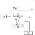
- a schematic diagram of sputter deposition apparatus 100 is shown in Figure 1 , and its operation will be briefly explained in the following.
- a gas source 110 is provided for a chamber 120, which is maintained at a low pressure by means of a vacuum pump 130.
- the gas is an inert gas, for example argon.
- the chamber holds a substrate 140, and a target 150.
- the process gas supplied from the gas source is ionised within the vacuum chamber 120, and the resulting positively charged ions 160 are accelerated towards the target 150 under the influence of an electric field due to anode 170.
- the ions collide with the target 150 to eject target material in the direction of the substrate 140.
- Target material collects on the substrate resulting in the growth of a thin film 180 of target material on the substrate 140.
- the rate of growth and the quality of the film 180 depend critically on the actual configuration of the sputtering apparatus that is used. A number of important parameters can be identified.
- the size and configuration of the chamber influences the cleanliness of the system through the out-gassing rate, which is partly determined by the surface-area to volume ratio of the chamber.
- the geometric relationship of the target to the substrate influences the thin film growth rate, and, through the path length between the target and the substrate, will affect the energy of the target material when incident on the substrate.
- the uniformity of the resulting thin film is also influenced as a result of geometric variation in the ejection of material from the target
- the choice of vacuum pump used will set the attainable base pressure in the system, therefore influencing the overall cleanliness of the system, and, through setting of the gas volume pump speed, determines the cleanliness of the process gas. These features in turn may influence the thin film morphology, for example by the pinning of grain boundaries at impurities, or influencing the density of nucleation sites.
- One example of a vacuum pump that can be used in sputtering systems is the cryo pump.
- the cryo pump uses liquid helium to solidify any gases present in the system, and, for sputtering systems, has the advantage that a relatively clean vacuum is produced.
- the choice of process gas determines the ease of plasma formation through the ionisation energy of the process gas, and also determines the kinetic energy of ejected target material through the atomic mass of the process gas.
- the choice of process gas pressure limits the actual energy of both ions incident on the target and target particles incident on the substrate through variation of the number of scattering collisions that take place in the chamber.
- the choice of target material influences deposition rate, uniformity and kinetic energy of ejected target material.
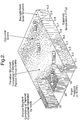
- Zone Model also known as the Thornton Model, that is described in J.A. Thornton, J. Vac. Sci. Technol. 11, p666 (1974 ), and that is schematically illustrated in Figure 2 .
- Zone T microstructure an additional transitional zone between zone I and II.
- the model describes how the microstructure of the thin film obtained changes in dependence on the conditions in which the film is sputtered, parameterising those conditions in terms of substrate temperature, measured relative to the melting point of the target material, and sputter pressure.
- Zone I microstructures obtained in low energy conditions (high pressure and low temperature), are characterised by a tapered grain structure, which arises out of a random set of nucleation sites at which growth occurs competitively, resulting in touching, domed "grains" that are not strongly inter-bonded. Under more energetic conditions (lower pressure and higher temperature), Zone T microstructures, and then Zone II microstructures are obtained. The transition between 1 and 11 occurs at a temperature of around 1 ⁇ 3 T m , as can be seen from Figure 2 . In the transitional zone, the grains are more densely packed than in Zone I, and have a fibrous structure. Zone II microstructures have a yet more densely packed, columnar grain structure that has faceted surfaces and much stronger inter-bonding between the grains.
- Zone III microstructures are obtained, in which there are larger, columnar grains.
- the transition from Zone I to Zone III microstructures occurs at around 1 ⁇ 2 T m , as can be seen from Figure 2 . It is noted that the transitional temperatures also vary with pressure resulting in the two dimensional zone model shown in Figure 2 .
- Zone II or Zone III microstructures are arranged to produce films that exhibit mechanical strength, high density, and low resistivity.
- getter devices open, porous structures having a high specific area are required, and therefore sputtered thin films having a Zone I microstructure are likely to be more effective getters.
- Less energetic conditions high pressure and/or lower temperatures are needed in order to manufacture effective getter devices.
- higher density structures will have a lower specific area, whilst lower density structures will have a higher specific area.
- FIG. 3 shows a schematic diagram of getter device 300 produced in accordance with a first embodiment of the invention.
- the getter device comprises substrate 320, and getter material in the form of a layer referenced generally 350, which layer comprises a first portion 340, and a cap portion 360.
- the getter material in the present embodiment is titanium, and the getter device is produced by sputtering titanium onto the substrate 320 to form the thin film 350, which is of the order of 1 ⁇ m thick.
- the main portion 340 of the layer, which forms the bulk of the thin film 350, is formed using sputtering conditions arranged, as described in further detail below, to result in an open, porous structure, with a high specific area, that will exhibit high getter activity.
- the cap portion 360 is much thinner than the main portion, of the order of 0.01 ⁇ m to 0.1 ⁇ m. It is formed using conditions arranged, as described in further detail below, to result in a denser microstructure having a lower specific area, and therefore a lower getter activity, than the main portion 340.
- the cap portion forms an external surface of the getter device, and so, when the getter device is exposed to atmospheric conditions, the getter material in the cap portion rapidly oxidises. However, since the cap portion has only limited porosity, the bulk of the getter device in the main portion 340 of the layer 350 is protected from oxidation when the device is handled under normal atmospheric conditions.
- the device 300 must be activated in order to function as a getter in a vacuum environment.
- the getter material in the first portion 340 must be exposed. Experiment has shown that this can be accomplished by heating the device to a temperature of 450 °C. It is currently thought that this activation is due either to thermal expansion of the getter device resulting in the grain structure of the cap portion 350 opening up and exposing the main portion 340, or because further grain growth at the higher temperature results in a coarsening of the grain structure that increases the intergrain porosity. Alternatively, the activation could be a result of diffusion of the thin surface layers of the cap portion in to the bulk, thereby exposing fresh material. Other mechanisms, however, may be responsible.
- the device 300 is fabricated in a CVC601 sputtering system obtained from CVC Products Inc., of 525 Lee Road, P.O. Box 1888, Rochester, N.Y. 14603, USA. It is a cryo-pumped batch-loaded multiple-substrate deposition machine, with three 8" Magnetron targets in a sputter up configuration.
- the substrates are held on a rotatable partially thermally isolated carousel, which can hold either twelve 4" wafers, or eight 5" wafers.
- Titanium films were deposited directly onto a silicon substrate, with a shadow mask used to define the position of the deposited getter layer. No sputter etch was carried out. No special measures were taken to ensure good adhesion of the titanium to the substrate, since titanium has a high reactivity and is therefore expected to chemically bond with the substrate surface. Experimentally, it was found that good adhesion was obtained under all deposition conditions.
- sputtering in less energetic conditions generally results in a more open, more porous structure that is preferable where gettering activity is desired.
- direct control of the substrate temperature is not possible, and so only indirect temperature control is possible.
- Such indirect control can be achieved by changing the sputtering power, which would result in a lower degree of self-heating, but is unlikely to be sufficient to provide the magnitude of temperature control necessary for significant microstructural changes to be achieved in the case of titanium, which has a high melting point (1660 °C).
- the temperature in the CVC601 system is neither precisely controllable nor precisely measurable.
- the sputter pressure can be controlled directly, and is also expected to result in significant changes to the microstructure of the resulting thin film.
- a microstructure having a more open structure and lower density is obtained.
- Such a microstructure exhibits a higher specific surface area available for gettering chemistry to occur.
- the first portion 340 of device 300 illustrated in Figure 3 is the first part of the film to be deposited onto the substrate, and is deposited using a sputter pressure of 14 mTorr, that is significantly greater than the 8 mTorr pressure used in the fabrication of standard thin titanium films, and using a sputter power of 500 W for 100 minutes to achieve a thickness of approximately 1 ⁇ m.
- the cap portion 360 is formed by reducing the sputter pressure to 8 mTorr and continuing deposition at 500 W for 1-10 minutes to achieve a cap thickness of approximately 0.01-0.1 ⁇ m. The cap portion is therefore significantly thinner than the first portion.
- both the cap portion 360 and the first portion 340 are therefore fabricated in one continuous deposition process, with the advantage that the first portion is not exposed to atmospheric conditions during fabrication. Post-fabrication, the first portion 340 is protected from atmospheric conditions by cap portion 360. Moreover, the fabrication of the device 300 can be carried out for lower cost than that of prior known protected getter devices since both the first, main portion of the device 300, and the protecting cap portion, are fabricated in a single continuous process using a single material.
- a getter device 500 produced in accordance with a second embodiment of the invention is shown in Figure 5 .
- the device 500 is very similar to the device 300 of the first embodiment shown in Figure 3 , and like parts are referenced with the same numerals as used in Figure 3 , with an increment of 200.
- Device 500 comprises a substrate 520, and a layer of getter material 550 that is shown divided into a main portion 540 and a cap portion 560.
- Device 500 differs significantly from device 300 only in cap portion 560, which has a graded density profile, so that there is no distinct line of demarcation between the structural properties of the main, porous, portion 540, and those of the cap portion 560, but instead a gradual increase in the density of the film on moving through the cap portion, from a first value equal to that of the main portion, to a second, higher value at the surface of the getter device. There is therefore a corresponding decrease in porosity on moving through the cap portion 560 to the surface of the getter device.
- the specific area of the microstructure of the getter device is continuous across the boundary between the main portion and the cap portion.
- Device 500 is fabricated in the CVC601 sputtering system as described above in relation to the fabrication of the device 300.
- the fabrication process is substantially the same, except in that the pressure is not switched from 14 mTorr to 8 mTorr during the last ten minutes of the sputtering process, but is instead linearly decreased from 14 mTorr to 8 mTorr during the last ten minutes of the sputtering process, to result in the graded structure of the cap portion 560 that is described above.
- Figure 6a shows the atomic percentages of titanium and oxygen in a number of as-deposited getter devices standard titanium film (results labelled 610), a porous titanium film (results labelled 620), a porous titanium film with a thin (uniform) cap of standard titanium film (results labelled 630), a porous titanium film with a thick (uniform) cap of standard titanium film (results labelled 640), and a porous titanium film with a graded cap (results labelled 650).
- the bar on the left hand side indicates the amount of titanium present in the films by atomic percentages and the bar on the right indicates the amount of oxygen present by atomic percentages.
- the thin cap has a thickness of approximately 0.01 ⁇ m, resulting from a deposition time of 1 minute, whilst the thick cap has a thickness of approximately 0.1 ⁇ m , resulting from a deposition time of 10 minutes.
- the standard metal film fabricated by deposition at 8 mTorr show the lowest oxygen incorporation (at 9.9% atomic).
- the porous metal film results labelled 620 show that the porous film has more than double the oxygen content of the standard metal film (approximately 22.3% atomic), demonstrating the improved porosity of films deposited at higher pressures.
- the capped structures (results labelled 630, 640, and 650) have significantly lower oxygen content (15.2% atomic, 15.5% atomic and 13.4% atomic for samples 630, 640, and 650 respectively) than the porous metal, but still greater oxygen incorporation than the standard metal films.
- the graded cap (results labelled 650) exhibits the lowest oxygen incorporation at approximately 13.4%.
- the porous film exhibits the lowest increase in oxygen content of 6.2%.
- the thick-capped sample exhibits a significantly larger increase in oxygen content of 13.9%, whilst the thin capped (results labelled 630) and the graded cap (results labelled 650) samples exhibit greater-still increases in oxygen content of 16.5% and 16.1% respectively.
- all the capping treatments significantly improve the gettering performance of the devices, as compared to the porous structure.
- the slightly poorer performance of the thick-capped structure is thought to be due to poorer break-up of the cap on heating to 450°C.
- Such gyroscope structures comprise a vibrating a silicon substantially planar ring vibrating structure and capacitive means for imparting drive motion to, and sensing motion of, the vibrating structure, as is disclosed in EP1163490 , and are suitable for manufacturing by micromachining techniques.
- the vibrating ring structure is enclosed within a vacuum package formed at a late stage in the manufacture of the gyroscope. It is necessary to ensure that the vibrating structure is in an ambient pressure that is kept as low as possible in order that the Q-factor of its oscillations is kept as high as possible.
- Getter devices as described above can be used to maintain a stable, low pressure in the package despite outgassing from other components of the structure.
- the getter is incorporated into the "lid" of the package, and activation occurs during the bonding of the lid to the base of the structure, on which the vibrating ring is formed.
- getter devices according to embodiments of the invention can readily be altered as desired through adjustment of the porosities of the various portions of the getter layers, the thickness of the cap portion, and the gradient of porosity applied to the cap portion through the control of the sputtering pressure.
- getter materials other than titanium, such as, for example, those getter materials disclosed hereinabove.
- the above sputtering parameter values are suitable for the CVC601 sputtering system described above, these parameters will not necessarily transfer immediately to other sputtering systems.
- the pressures used for the above-described embodiments of the invention cannot be simply carried over to other sputtering systems since the absolute pressure value necessary to achieve the optimum microstructure will vary with the other parameters of the sputtering system as is described above.
Landscapes
- Chemical & Material Sciences (AREA)
- Organic Chemistry (AREA)
- Chemical Kinetics & Catalysis (AREA)
- Analytical Chemistry (AREA)
- Engineering & Computer Science (AREA)
- Microelectronics & Electronic Packaging (AREA)
- Materials Engineering (AREA)
- Metallurgy (AREA)
- Inorganic Chemistry (AREA)
- Mechanical Engineering (AREA)
- General Physics & Mathematics (AREA)
- Remote Sensing (AREA)
- Radar, Positioning & Navigation (AREA)
- Computer Hardware Design (AREA)
- Physics & Mathematics (AREA)
- Dispersion Chemistry (AREA)
- Physical Vapour Deposition (AREA)
- Gyroscopes (AREA)
- Solid-Sorbent Or Filter-Aiding Compositions (AREA)
Claims (5)
- Procédé de fabrication et d'activation d'un dispositif à sorbeur en film mince (300) comprenant la pulvérisation d'un matériau sorbeur sur un substrat (320), la pulvérisation comprenant les étapes suivantes :(a) la pulvérisation d'une partie principale (340) du matériau sorbeur en utilisant un premier ensemble de conditions de pulvérisation ;(b) la pulvérisation d'une partie de coiffe (360) du matériau sorbeur en utilisant un second ensemble de conditions de pulvérisation ; dans lequelle premier ensemble de conditions de pulvérisation comprenant une première pression, et le second ensemble de conditions de pulvérisation comprenant une seconde pression plus basse ou
le premier ensemble de conditions de pulvérisation est configuré pour produire une couche résultante (340) de matériau sorbeur d'une plus grande surface spécifique que celle produite en utilisant le second ensemble de conditions de pulvérisation ;
le premier ensemble de conditions de pulvérisation comprenant une température plus basse que le second ensemble de conditions de pulvérisation ; et dans lequel
la partie de coiffe (360) et la partie principale (340) sont constituées du même matériau sorbeur et la première partie (340) est protégée de conditions atmosphériques par la partie de coiffe (360) ; et dans lequel le procédé comprend en outre :
(c) l'installation du dispositif à sorbeur (300) dans un environnement de vide et l'activation du dispositif en exposant le matériau sorbeur. - Procédé selon la revendication 1, dans lequel la partie principale (340) et la partie de coiffe (360) sont fabriquées dans un seul processus de dépôt continu.
- Procédé selon la revendication 1 ou 2, dans lequel le matériau sorbeur est du titane.
- Procédé selon l'une quelconque des revendications précédentes, dans lequel le premier ensemble de conditions de pulvérisation comprend une première pression, et le second ensemble de conditions de pulvérisation comprend une seconde pression plus basse.
- Procédé selon l'une quelconque des revendications précédentes, dans lequel l'activation du dispositif implique le chauffage du dispositif à sorbeur à 450 °C.
Priority Applications (1)
| Application Number | Priority Date | Filing Date | Title |
|---|---|---|---|
| EP07824741.8A EP2126155B1 (fr) | 2006-12-15 | 2007-11-28 | Améliorations de dispositifs améliorés à sorbeurs en film mince |
Applications Claiming Priority (4)
| Application Number | Priority Date | Filing Date | Title |
|---|---|---|---|
| GB0625060A GB0625060D0 (en) | 2006-12-15 | 2006-12-15 | Improvements relating to thin film getter devices |
| EP06270102 | 2006-12-15 | ||
| PCT/GB2007/004559 WO2008071906A1 (fr) | 2006-12-15 | 2007-11-28 | Améliorations de dispositifs améliorés à sorbeurs en film mince |
| EP07824741.8A EP2126155B1 (fr) | 2006-12-15 | 2007-11-28 | Améliorations de dispositifs améliorés à sorbeurs en film mince |
Publications (2)
| Publication Number | Publication Date |
|---|---|
| EP2126155A1 EP2126155A1 (fr) | 2009-12-02 |
| EP2126155B1 true EP2126155B1 (fr) | 2019-03-13 |
Family
ID=38924456
Family Applications (1)
| Application Number | Title | Priority Date | Filing Date |
|---|---|---|---|
| EP07824741.8A Active EP2126155B1 (fr) | 2006-12-15 | 2007-11-28 | Améliorations de dispositifs améliorés à sorbeurs en film mince |
Country Status (4)
| Country | Link |
|---|---|
| US (1) | US8663789B2 (fr) |
| EP (1) | EP2126155B1 (fr) |
| JP (1) | JP2009522104A (fr) |
| WO (1) | WO2008071906A1 (fr) |
Families Citing this family (13)
| Publication number | Priority date | Publication date | Assignee | Title |
|---|---|---|---|---|
| FR2952627A1 (fr) | 2009-11-17 | 2011-05-20 | Commissariat Energie Atomique | Getter ayant deux temperatures d'activation et structure comportant ce getter |
| FR2976933B1 (fr) | 2011-06-23 | 2014-06-06 | Commissariat Energie Atomique | Structure getter comportant un materiau permeable aux gaz |
| FR2977883B1 (fr) * | 2011-07-11 | 2014-03-14 | Commissariat Energie Atomique | Structure getter a capacite de pompage optimisee |
| US9196556B2 (en) * | 2014-02-28 | 2015-11-24 | Raytheon Company | Getter structure and method for forming such structure |
| JP6209270B2 (ja) * | 2014-04-03 | 2017-10-04 | 日立オートモティブシステムズ株式会社 | 加速度センサ |
| US11524271B2 (en) * | 2017-08-28 | 2022-12-13 | Industry-University Cooperation Foundation Hanyang University Erica Campus | Thin film getter and manufacturing method therefor |
| CN108039314A (zh) * | 2017-12-08 | 2018-05-15 | 米亚索乐装备集成(福建)有限公司 | 叠层薄膜的制备方法和叠层薄膜 |
| AU2020256199B2 (en) | 2019-04-01 | 2022-12-15 | The Regents Of The University Of Colorado, A Body Corporate | Device and method for wireless microstimulation |
| JP7510640B2 (ja) | 2019-12-17 | 2024-07-04 | 国立研究開発法人産業技術総合研究所 | 反射防止構造体、及びその製造方法 |
| CN113337800A (zh) * | 2020-03-02 | 2021-09-03 | 杭州海康微影传感科技有限公司 | 薄膜吸气剂及其制备方法 |
| CN117535632A (zh) * | 2020-04-01 | 2024-02-09 | 佳能安内华股份有限公司 | 成膜设备、控制设备以及成膜方法 |
| CN111892014B (zh) * | 2020-07-30 | 2023-10-31 | 钢铁研究总院 | 一种吸气薄膜及其制备方法 |
| FR3128232A1 (fr) * | 2021-10-14 | 2023-04-21 | Safran Electronics & Defense | Procédé de fabrication d’un élément de pompage comprenant la réalisation d’un dépôt de matériau getter par pulvérisation par faisceau d’ions |
Citations (1)
| Publication number | Priority date | Publication date | Assignee | Title |
|---|---|---|---|---|
| US6258219B1 (en) * | 1993-09-09 | 2001-07-10 | Applied Materials, Inc. | Two-step deposition process for preventing arcs |
Family Cites Families (17)
| Publication number | Priority date | Publication date | Assignee | Title |
|---|---|---|---|---|
| JPH0624629B2 (ja) * | 1990-02-09 | 1994-04-06 | 科学技術庁金属材料技術研究所長 | 内部拡散薄膜型ゲッター材料 |
| TW287117B (fr) * | 1994-12-02 | 1996-10-01 | Getters Spa | |
| US5814241A (en) * | 1994-12-29 | 1998-09-29 | Tovarischetstvo S Organichennoi Otvetstvennostju "Tekhnovakt" | Non-vaporizing getter and method of obtaining the same |
| JPH1187651A (ja) * | 1997-09-08 | 1999-03-30 | Hitachi Ltd | 半導体集積回路装置およびその製造方法 |
| GB9828478D0 (en) | 1998-12-24 | 1999-02-17 | British Aerospace | Method of manufacturing a vibrating structure gyroscope |
| JP3518855B2 (ja) * | 1999-02-26 | 2004-04-12 | キヤノン株式会社 | ゲッター、ゲッターを有する気密容器および画像形成装置、ゲッターの製造方法 |
| IT1318937B1 (it) * | 2000-09-27 | 2003-09-19 | Getters Spa | Metodo per la produzione di dispositivi getter porosi con ridottaperdita di particelle e dispositivi cosi' prodotti |
| JP2003022744A (ja) * | 2001-07-06 | 2003-01-24 | Sony Corp | 非蒸発型ゲッター、表示装置およびこれらの製造方法 |
| TW583049B (en) | 2001-07-20 | 2004-04-11 | Getters Spa | Support with integrated deposit of gas absorbing material for manufacturing microelectronic, microoptoelectronic or micromechanical devices |
| US6992442B2 (en) | 2001-12-11 | 2006-01-31 | Honeywell International Inc. | Restricted getter |
| US6923625B2 (en) | 2002-01-07 | 2005-08-02 | Integrated Sensing Systems, Inc. | Method of forming a reactive material and article formed thereby |
| US6914323B2 (en) * | 2003-03-20 | 2005-07-05 | Honeywell International Inc. | Methods and apparatus for attaching getters to MEMS device housings |
| US6988924B2 (en) * | 2003-04-14 | 2006-01-24 | Hewlett-Packard Development Company, L.P. | Method of making a getter structure |
| ITMI20031178A1 (it) | 2003-06-11 | 2004-12-12 | Getters Spa | Depositi multistrato getter non evaporabili ottenuti per |
| JP2005016965A (ja) * | 2003-06-23 | 2005-01-20 | Sumitomo Precision Prod Co Ltd | パッケージおよびその製造方法、ならびに振動ジャイロおよびその製造方法 |
| DE102005001449B3 (de) * | 2005-01-12 | 2006-07-20 | Fraunhofer-Gesellschaft zur Förderung der angewandten Forschung e.V. | Verfahren zum Erzeugen eines vorgegebenen Innendrucks in einem Hohlraum eines Halbleiterbauelements |
| KR20100005255U (ko) | 2005-02-17 | 2010-05-20 | 세스 게터스 에스.피.에이 | 플렉시블 다층 게터 |
-
2007
- 2007-11-28 JP JP2008549936A patent/JP2009522104A/ja active Pending
- 2007-11-28 US US12/159,828 patent/US8663789B2/en active Active
- 2007-11-28 WO PCT/GB2007/004559 patent/WO2008071906A1/fr not_active Ceased
- 2007-11-28 EP EP07824741.8A patent/EP2126155B1/fr active Active
Patent Citations (1)
| Publication number | Priority date | Publication date | Assignee | Title |
|---|---|---|---|---|
| US6258219B1 (en) * | 1993-09-09 | 2001-07-10 | Applied Materials, Inc. | Two-step deposition process for preventing arcs |
Also Published As
| Publication number | Publication date |
|---|---|
| US20090081434A1 (en) | 2009-03-26 |
| WO2008071906A1 (fr) | 2008-06-19 |
| JP2009522104A (ja) | 2009-06-11 |
| US8663789B2 (en) | 2014-03-04 |
| EP2126155A1 (fr) | 2009-12-02 |
Similar Documents
| Publication | Publication Date | Title |
|---|---|---|
| EP2126155B1 (fr) | Améliorations de dispositifs améliorés à sorbeurs en film mince | |
| US6923625B2 (en) | Method of forming a reactive material and article formed thereby | |
| US7786561B2 (en) | Encapsulated microcomponent equipped with at least one getter | |
| US9637377B2 (en) | Method for forming a micro-surface structure and for producing a micro-electromechanical component | |
| JP2016047595A (ja) | マイクロエレクトロニクス、マイクロオプトエレクトロニクスまたはマイクロメカニクスのデバイスのための支持体 | |
| CN101611465B (zh) | 空气稳定的碱金属或碱土金属释放体 | |
| JP4831931B2 (ja) | マイクロエレクトロニクス、マイクロオプトエレクトロニクスまたはマイクロメカニクスのデバイスを製造するための気体吸収物質の集積堆積物を有する支持体 | |
| US20090001537A1 (en) | Gettering material for encapsulated microdevices and method of manufacture | |
| KR20100135957A (ko) | 몰리브덴-니오브 합금, 몰리브덴-니오브 합금을 포함하는 스퍼터링 타겟, 이러한 스퍼터링 타겟의 제조 방법 및 이러한 스퍼터링 타겟으로부터 준비되는 박막 및 그 용도 | |
| US7147908B2 (en) | Semiconductor package with getter formed over an irregular structure | |
| JP5661452B2 (ja) | スパッタリング方法 | |
| US20190382263A1 (en) | Method for producing a system including a first microelectromechanical element and a second microelectromechanical element, and a system | |
| JP4971305B2 (ja) | 小型ゲッタ蒸着層の形成方法 | |
| Wu et al. | Oblique angle deposition of Au/Ti porous getter films | |
| KR20210027394A (ko) | 게터를 포함하는 밀폐된 패키지, 이러한 밀폐된 패키지를 포함하는 부품 및 관련 제조 공정 | |
| Yamazaki et al. | Effective surface area of SnO2-sputtered films evaluated by measurement of physical adsorption isotherms | |
| CN115323334B (zh) | 一种溅射方法及溅射装置 | |
| JP3989083B2 (ja) | 真空容器 | |
| EP4143874B1 (fr) | Appareil et procédés de scellement hermétique de mems | |
| JP4670613B2 (ja) | 成膜方法及び成膜装置、並びに成膜用ターゲット | |
| WO2019136261A1 (fr) | Co-dépôt en phase gazeuse de structures métalliques chargées d'hydrogène/deutérium | |
| EP4504647A1 (fr) | Substrat comprenant une base et un film getter intégré pour fabriquer des dispositifs microélectroniques | |
| CN115404437A (zh) | 溅射方法和溅射设备 | |
| Shaalan et al. | Nanostructure of WO3 sputtered films deposited at various gas pressures | |
| JPS59141219A (ja) | 薄膜の作製方法 |
Legal Events
| Date | Code | Title | Description |
|---|---|---|---|
| PUAI | Public reference made under article 153(3) epc to a published international application that has entered the european phase |
Free format text: ORIGINAL CODE: 0009012 |
|
| 17P | Request for examination filed |
Effective date: 20090616 |
|
| AK | Designated contracting states |
Kind code of ref document: A1 Designated state(s): AT BE BG CH CY CZ DE DK EE ES FI FR GB GR HU IE IS IT LI LT LU LV MC MT NL PL PT RO SE SI SK TR |
|
| DAX | Request for extension of the european patent (deleted) | ||
| 17Q | First examination report despatched |
Effective date: 20100407 |
|
| GRAP | Despatch of communication of intention to grant a patent |
Free format text: ORIGINAL CODE: EPIDOSNIGR1 |
|
| STAA | Information on the status of an ep patent application or granted ep patent |
Free format text: STATUS: GRANT OF PATENT IS INTENDED |
|
| INTG | Intention to grant announced |
Effective date: 20181121 |
|
| GRAS | Grant fee paid |
Free format text: ORIGINAL CODE: EPIDOSNIGR3 |
|
| GRAA | (expected) grant |
Free format text: ORIGINAL CODE: 0009210 |
|
| STAA | Information on the status of an ep patent application or granted ep patent |
Free format text: STATUS: THE PATENT HAS BEEN GRANTED |
|
| AK | Designated contracting states |
Kind code of ref document: B1 Designated state(s): AT BE BG CH CY CZ DE DK EE ES FI FR GB GR HU IE IS IT LI LT LU LV MC MT NL PL PT RO SE SI SK TR |
|
| REG | Reference to a national code |
Ref country code: GB Ref legal event code: FG4D |
|
| REG | Reference to a national code |
Ref country code: CH Ref legal event code: EP Ref country code: AT Ref legal event code: REF Ref document number: 1107755 Country of ref document: AT Kind code of ref document: T Effective date: 20190315 |
|
| REG | Reference to a national code |
Ref country code: IE Ref legal event code: FG4D |
|
| REG | Reference to a national code |
Ref country code: DE Ref legal event code: R096 Ref document number: 602007057844 Country of ref document: DE |
|
| REG | Reference to a national code |
Ref country code: NL Ref legal event code: FP |
|
| REG | Reference to a national code |
Ref country code: LT Ref legal event code: MG4D |
|
| PG25 | Lapsed in a contracting state [announced via postgrant information from national office to epo] |
Ref country code: FI Free format text: LAPSE BECAUSE OF FAILURE TO SUBMIT A TRANSLATION OF THE DESCRIPTION OR TO PAY THE FEE WITHIN THE PRESCRIBED TIME-LIMIT Effective date: 20190313 Ref country code: SE Free format text: LAPSE BECAUSE OF FAILURE TO SUBMIT A TRANSLATION OF THE DESCRIPTION OR TO PAY THE FEE WITHIN THE PRESCRIBED TIME-LIMIT Effective date: 20190313 Ref country code: LT Free format text: LAPSE BECAUSE OF FAILURE TO SUBMIT A TRANSLATION OF THE DESCRIPTION OR TO PAY THE FEE WITHIN THE PRESCRIBED TIME-LIMIT Effective date: 20190313 |
|
| PG25 | Lapsed in a contracting state [announced via postgrant information from national office to epo] |
Ref country code: BG Free format text: LAPSE BECAUSE OF FAILURE TO SUBMIT A TRANSLATION OF THE DESCRIPTION OR TO PAY THE FEE WITHIN THE PRESCRIBED TIME-LIMIT Effective date: 20190613 Ref country code: GR Free format text: LAPSE BECAUSE OF FAILURE TO SUBMIT A TRANSLATION OF THE DESCRIPTION OR TO PAY THE FEE WITHIN THE PRESCRIBED TIME-LIMIT Effective date: 20190614 Ref country code: LV Free format text: LAPSE BECAUSE OF FAILURE TO SUBMIT A TRANSLATION OF THE DESCRIPTION OR TO PAY THE FEE WITHIN THE PRESCRIBED TIME-LIMIT Effective date: 20190313 |
|
| REG | Reference to a national code |
Ref country code: AT Ref legal event code: MK05 Ref document number: 1107755 Country of ref document: AT Kind code of ref document: T Effective date: 20190313 |
|
| PG25 | Lapsed in a contracting state [announced via postgrant information from national office to epo] |
Ref country code: EE Free format text: LAPSE BECAUSE OF FAILURE TO SUBMIT A TRANSLATION OF THE DESCRIPTION OR TO PAY THE FEE WITHIN THE PRESCRIBED TIME-LIMIT Effective date: 20190313 Ref country code: PT Free format text: LAPSE BECAUSE OF FAILURE TO SUBMIT A TRANSLATION OF THE DESCRIPTION OR TO PAY THE FEE WITHIN THE PRESCRIBED TIME-LIMIT Effective date: 20190713 Ref country code: CZ Free format text: LAPSE BECAUSE OF FAILURE TO SUBMIT A TRANSLATION OF THE DESCRIPTION OR TO PAY THE FEE WITHIN THE PRESCRIBED TIME-LIMIT Effective date: 20190313 Ref country code: SK Free format text: LAPSE BECAUSE OF FAILURE TO SUBMIT A TRANSLATION OF THE DESCRIPTION OR TO PAY THE FEE WITHIN THE PRESCRIBED TIME-LIMIT Effective date: 20190313 Ref country code: RO Free format text: LAPSE BECAUSE OF FAILURE TO SUBMIT A TRANSLATION OF THE DESCRIPTION OR TO PAY THE FEE WITHIN THE PRESCRIBED TIME-LIMIT Effective date: 20190313 Ref country code: ES Free format text: LAPSE BECAUSE OF FAILURE TO SUBMIT A TRANSLATION OF THE DESCRIPTION OR TO PAY THE FEE WITHIN THE PRESCRIBED TIME-LIMIT Effective date: 20190313 |
|
| PG25 | Lapsed in a contracting state [announced via postgrant information from national office to epo] |
Ref country code: PL Free format text: LAPSE BECAUSE OF FAILURE TO SUBMIT A TRANSLATION OF THE DESCRIPTION OR TO PAY THE FEE WITHIN THE PRESCRIBED TIME-LIMIT Effective date: 20190313 |
|
| REG | Reference to a national code |
Ref country code: DE Ref legal event code: R097 Ref document number: 602007057844 Country of ref document: DE |
|
| PG25 | Lapsed in a contracting state [announced via postgrant information from national office to epo] |
Ref country code: AT Free format text: LAPSE BECAUSE OF FAILURE TO SUBMIT A TRANSLATION OF THE DESCRIPTION OR TO PAY THE FEE WITHIN THE PRESCRIBED TIME-LIMIT Effective date: 20190313 Ref country code: IS Free format text: LAPSE BECAUSE OF FAILURE TO SUBMIT A TRANSLATION OF THE DESCRIPTION OR TO PAY THE FEE WITHIN THE PRESCRIBED TIME-LIMIT Effective date: 20190713 |
|
| PLBE | No opposition filed within time limit |
Free format text: ORIGINAL CODE: 0009261 |
|
| STAA | Information on the status of an ep patent application or granted ep patent |
Free format text: STATUS: NO OPPOSITION FILED WITHIN TIME LIMIT |
|
| PG25 | Lapsed in a contracting state [announced via postgrant information from national office to epo] |
Ref country code: DK Free format text: LAPSE BECAUSE OF FAILURE TO SUBMIT A TRANSLATION OF THE DESCRIPTION OR TO PAY THE FEE WITHIN THE PRESCRIBED TIME-LIMIT Effective date: 20190313 |
|
| 26N | No opposition filed |
Effective date: 20191216 |
|
| PG25 | Lapsed in a contracting state [announced via postgrant information from national office to epo] |
Ref country code: SI Free format text: LAPSE BECAUSE OF FAILURE TO SUBMIT A TRANSLATION OF THE DESCRIPTION OR TO PAY THE FEE WITHIN THE PRESCRIBED TIME-LIMIT Effective date: 20190313 |
|
| PG25 | Lapsed in a contracting state [announced via postgrant information from national office to epo] |
Ref country code: TR Free format text: LAPSE BECAUSE OF FAILURE TO SUBMIT A TRANSLATION OF THE DESCRIPTION OR TO PAY THE FEE WITHIN THE PRESCRIBED TIME-LIMIT Effective date: 20190313 |
|
| REG | Reference to a national code |
Ref country code: CH Ref legal event code: PL |
|
| PG25 | Lapsed in a contracting state [announced via postgrant information from national office to epo] |
Ref country code: LU Free format text: LAPSE BECAUSE OF NON-PAYMENT OF DUE FEES Effective date: 20191128 Ref country code: LI Free format text: LAPSE BECAUSE OF NON-PAYMENT OF DUE FEES Effective date: 20191130 Ref country code: CH Free format text: LAPSE BECAUSE OF NON-PAYMENT OF DUE FEES Effective date: 20191130 Ref country code: MC Free format text: LAPSE BECAUSE OF FAILURE TO SUBMIT A TRANSLATION OF THE DESCRIPTION OR TO PAY THE FEE WITHIN THE PRESCRIBED TIME-LIMIT Effective date: 20190313 |
|
| REG | Reference to a national code |
Ref country code: BE Ref legal event code: MM Effective date: 20191130 |
|
| PG25 | Lapsed in a contracting state [announced via postgrant information from national office to epo] |
Ref country code: IE Free format text: LAPSE BECAUSE OF NON-PAYMENT OF DUE FEES Effective date: 20191128 |
|
| PG25 | Lapsed in a contracting state [announced via postgrant information from national office to epo] |
Ref country code: BE Free format text: LAPSE BECAUSE OF NON-PAYMENT OF DUE FEES Effective date: 20191130 |
|
| PG25 | Lapsed in a contracting state [announced via postgrant information from national office to epo] |
Ref country code: CY Free format text: LAPSE BECAUSE OF FAILURE TO SUBMIT A TRANSLATION OF THE DESCRIPTION OR TO PAY THE FEE WITHIN THE PRESCRIBED TIME-LIMIT Effective date: 20190313 |
|
| PG25 | Lapsed in a contracting state [announced via postgrant information from national office to epo] |
Ref country code: HU Free format text: LAPSE BECAUSE OF FAILURE TO SUBMIT A TRANSLATION OF THE DESCRIPTION OR TO PAY THE FEE WITHIN THE PRESCRIBED TIME-LIMIT; INVALID AB INITIO Effective date: 20071128 Ref country code: MT Free format text: LAPSE BECAUSE OF FAILURE TO SUBMIT A TRANSLATION OF THE DESCRIPTION OR TO PAY THE FEE WITHIN THE PRESCRIBED TIME-LIMIT Effective date: 20190313 |
|
| PGFP | Annual fee paid to national office [announced via postgrant information from national office to epo] |
Ref country code: NL Payment date: 20251022 Year of fee payment: 19 |
|
| PGFP | Annual fee paid to national office [announced via postgrant information from national office to epo] |
Ref country code: DE Payment date: 20251022 Year of fee payment: 19 |
|
| PGFP | Annual fee paid to national office [announced via postgrant information from national office to epo] |
Ref country code: GB Payment date: 20251022 Year of fee payment: 19 |
|
| PGFP | Annual fee paid to national office [announced via postgrant information from national office to epo] |
Ref country code: IT Payment date: 20251022 Year of fee payment: 19 |
|
| PGFP | Annual fee paid to national office [announced via postgrant information from national office to epo] |
Ref country code: FR Payment date: 20251022 Year of fee payment: 19 |