EP2129201B1 - Mehrschichtiges schaltungssubstrat - Google Patents
Mehrschichtiges schaltungssubstrat Download PDFInfo
- Publication number
- EP2129201B1 EP2129201B1 EP08711655.4A EP08711655A EP2129201B1 EP 2129201 B1 EP2129201 B1 EP 2129201B1 EP 08711655 A EP08711655 A EP 08711655A EP 2129201 B1 EP2129201 B1 EP 2129201B1
- Authority
- EP
- European Patent Office
- Prior art keywords
- basic material
- constrained
- layer
- conductor pattern
- material layer
- Prior art date
- Legal status (The legal status is an assumption and is not a legal conclusion. Google has not performed a legal analysis and makes no representation as to the accuracy of the status listed.)
- Not-in-force
Links
Images


Classifications
-
- H—ELECTRICITY
- H05—ELECTRIC TECHNIQUES NOT OTHERWISE PROVIDED FOR
- H05K—PRINTED CIRCUITS; CASINGS OR CONSTRUCTIONAL DETAILS OF ELECTRIC APPARATUS; MANUFACTURE OF ASSEMBLAGES OF ELECTRICAL COMPONENTS
- H05K1/00—Printed circuits
- H05K1/02—Details
- H05K1/11—Printed elements for providing electric connections to or between printed circuits
- H05K1/115—Via connections; Lands around holes or via connections
-
- H—ELECTRICITY
- H05—ELECTRIC TECHNIQUES NOT OTHERWISE PROVIDED FOR
- H05K—PRINTED CIRCUITS; CASINGS OR CONSTRUCTIONAL DETAILS OF ELECTRIC APPARATUS; MANUFACTURE OF ASSEMBLAGES OF ELECTRICAL COMPONENTS
- H05K1/00—Printed circuits
- H05K1/02—Details
- H05K1/0271—Arrangements for reducing stress or warp in rigid printed circuit boards, e.g. caused by loads, vibrations or differences in thermal expansion
-
- H—ELECTRICITY
- H05—ELECTRIC TECHNIQUES NOT OTHERWISE PROVIDED FOR
- H05K—PRINTED CIRCUITS; CASINGS OR CONSTRUCTIONAL DETAILS OF ELECTRIC APPARATUS; MANUFACTURE OF ASSEMBLAGES OF ELECTRICAL COMPONENTS
- H05K3/00—Apparatus or processes for manufacturing printed circuits
- H05K3/46—Manufacturing multilayer circuits
- H05K3/4611—Manufacturing multilayer circuits by laminating two or more circuit boards
- H05K3/4626—Manufacturing multilayer circuits by laminating two or more circuit boards characterised by the insulating layers or materials
- H05K3/4629—Manufacturing multilayer circuits by laminating two or more circuit boards characterised by the insulating layers or materials laminating inorganic sheets comprising printed circuits, e.g. green ceramic sheets
-
- H—ELECTRICITY
- H05—ELECTRIC TECHNIQUES NOT OTHERWISE PROVIDED FOR
- H05K—PRINTED CIRCUITS; CASINGS OR CONSTRUCTIONAL DETAILS OF ELECTRIC APPARATUS; MANUFACTURE OF ASSEMBLAGES OF ELECTRICAL COMPONENTS
- H05K1/00—Printed circuits
- H05K1/02—Details
- H05K1/03—Use of materials for the substrate
- H05K1/0306—Inorganic insulating substrates, e.g. ceramic, glass
-
- H—ELECTRICITY
- H05—ELECTRIC TECHNIQUES NOT OTHERWISE PROVIDED FOR
- H05K—PRINTED CIRCUITS; CASINGS OR CONSTRUCTIONAL DETAILS OF ELECTRIC APPARATUS; MANUFACTURE OF ASSEMBLAGES OF ELECTRICAL COMPONENTS
- H05K2201/00—Indexing scheme relating to printed circuits covered by H05K1/00
- H05K2201/01—Dielectrics
- H05K2201/0183—Dielectric layers
- H05K2201/0195—Dielectric or adhesive layers comprising a plurality of layers, e.g. in a multilayer structure
-
- H—ELECTRICITY
- H05—ELECTRIC TECHNIQUES NOT OTHERWISE PROVIDED FOR
- H05K—PRINTED CIRCUITS; CASINGS OR CONSTRUCTIONAL DETAILS OF ELECTRIC APPARATUS; MANUFACTURE OF ASSEMBLAGES OF ELECTRICAL COMPONENTS
- H05K2201/00—Indexing scheme relating to printed circuits covered by H05K1/00
- H05K2201/09—Shape and layout
- H05K2201/09209—Shape and layout details of conductors
- H05K2201/09654—Shape and layout details of conductors covering at least two types of conductors provided for in H05K2201/09218 - H05K2201/095
- H05K2201/09781—Dummy conductors, i.e. not used for normal transport of current; Dummy electrodes of components
-
- H—ELECTRICITY
- H05—ELECTRIC TECHNIQUES NOT OTHERWISE PROVIDED FOR
- H05K—PRINTED CIRCUITS; CASINGS OR CONSTRUCTIONAL DETAILS OF ELECTRIC APPARATUS; MANUFACTURE OF ASSEMBLAGES OF ELECTRICAL COMPONENTS
- H05K2201/00—Indexing scheme relating to printed circuits covered by H05K1/00
- H05K2201/10—Details of components or other objects attached to or integrated in a printed circuit board
- H05K2201/10227—Other objects, e.g. metallic pieces
- H05K2201/10378—Interposers
Definitions
- the present invention relates to a multilayer wiring board and, in particular, to a multilayer wiring board including base material layers and constrained layers that are alternately stacked.
- a multilayer wiring board 110 has been produced by stacking and pressing constrained layers 103a to 103d, each sandwiched between neighboring ones of the glass ceramic green sheet groups 102a to 102e each consisting of one layer or more.
- the glass ceramic green sheet groups 102a to 102e serve as basic material layers.
- the constrained layers 103a to 103d are formed of an inorganic composition that is not sintered under a firing condition of the glass ceramic green sheet groups 102a to 102e.
- a conductor pattern serving as one of internal electrodes 105a to 105d or one of external electrodes 107 and 108 is formed on a surface of one of the glass ceramic green sheet groups 102a to 102e and the constrained layers 103a to 103d.
- Through-holes that pass through the glass ceramic green sheet groups 102a to 102e are filled with conductive materials serving as via-hole conductors 104a to 104e, respectively. Subsequently, the glass ceramic green sheet groups 102a to 102e are fired.
- the constrained layers 103a to 103d negligibly contract when being fired.
- Patent Document 1 Japanese Unexamined Patent Application Publication No. 2000-315864
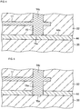
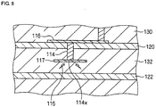
- a conductor pattern 116 is disposed on a surface of a constrained layer 120 or a basic material layer 130 and a wiring electrode 117 used for required connection is disposed in a basic material layer 132 (in the middle of the basic material layer 132) located between constrained layers 120 and 122 and if one end of a via-hole conductor 114 is connected to the wiring electrode 117, cracking 115 may occur in the basic material layer 132 in the vicinity of an end 114x of the via-hole conductor 114, that is, in the vicinity of a connection portion between the via-hole conductor 114 and the wiring electrode 117.
- the cracking 115 occurs because, although contraction of portions of the basic material layer 132 in contact with the constrained layers 120 and 122 in the surface direction is sufficiently prevented during a firing process, portions remote from the constrained layers 120 and 122 are not sufficiently constrained by the constrained layers 120 and 122. Accordingly, the portions remote from the constrained layers 120 and 122 also contract in the surface direction. That is, when the via-hole conductor 114 is disposed in the basic material layer 132 and if the via-hole conductor 114 extends to the middle of the basic material layer 132, a complicated contraction force that pulls the basic material layer 132 is exerted against a portion in the vicinity of the end 114x of the via-hole conductor 114.
- US-A-4,910,643 describes a thick film, multi-layer interconnected circuit board which includes a substrate of an electrical insulating material which will withstand high temperatures, such as alumina, having over a surface thereof a plurality of stacked layers of a glass dielectric. Between each pair of dielectric layers is a thick film conductor layer. The dielectric layers have openings or vias therethrough which are filled with a conductive material which makes electrical contact with the adjacent conductive layers. A contact pad is over the topmost dielectric layer and is electrically connected to a via conductor material in the topmost dielectric layer.
- the contact pad is of a thick film conductive material which is a layer of glass having particles of a conductive material, such as a noble metal or mixture of noble metals, dispersed therein.
- a bonding layer is between the contact pad and the topmost dielectric layer and is bonded to both.
- the bonding layer is of a mixture of the glass of the dielectric layers and the thick film conductive material of the contact pad.
- JP 2001 160 681 A which is considered to represent the closest prior art discloses a multilayer wiring board with basic material layers and constrained layers alternately stacked.
- a via connects to an intermediate conductor pattern disposed inside the basic material and further through the constrained layer so as to connect to a conductor pattern on the constrained layer.
- the present invention provides a multilayer wiring board having the following structure.
- a multilayer wiring board includes (a) at least one basic material layer and at least one constrained layer that are alternately stacked, (b) a conductor pattern disposed on or inside the basic material layer or the constrained layer, where the conductor pattern extends in a surface direction in which the basic material layer and the constrained layer extend, and (c) a via-hole conductor extending inside at least the basic material layer in a direction in which the basic material layer and the constrained layer are stacked, where the via-hole conductor is connected to the conductor pattern.
- the via-hole conductor includes a via body and an extended portion, the via body is connected to an intermediate conductor pattern disposed inside the basic material layer among the conductor patterns, and the extended portion is formed by extending the via body in a direction towards the constrained layer and away from the via body, and the extended portion is connected to the intermediate conductor pattern.
- one end of the via-hole conductor connected to the intermediate conductor pattern disposed inside the basic material layer is extended to the intermediate conductor pattern so that a via body is formed. Accordingly, the end of the via-hole conductor terminates at a position (a middle position) inside the basic material layer (at the middle position of the basic material layer).
- an extended portion is formed so that the via-hole conductor extends completely through the basic material layer and reaches the constrained layer. The extended portion of the via-hole conductor allows two via-hole conductor portions to be disposed on either side of the intermediate conductor pattern in the basic material layer.
- the contraction behaviors of the ceramic green sheet that forms the basic material layer on either side of the intermediate conductor pattern can be made substantially the same.
- the difference between the contraction behaviors can be reduced.
- the occurrence of cracking in the vicinity of a connection portion between the via-hole conductor and the intermediate conductor pattern can be prevented.
- the extended portion of the via-hole conductor is in contact with the constrained layer.
- the extended portion of the via-hole conductor is in contact with the constrained layer, the extended portion is also supported by the constrained layer. Accordingly, contraction of the extended portion in the plane direction can be constrained. As a result, the occurrence of cracking starting from the extended portion can be prevented.
- the multilayer wiring board can be formed so as to have the following various structures.
- the extended portion of the via-hole conductor extends completely through the constrained layer.
- the position of the via-hole conductor can be reliably maintained by the constrained layer.
- a precision-made multilayer wiring board can be provided.
- an end surface of the extended portion of the via-hole conductor is in contact with the constrained layer.
- the distance between the intermediate conductor pattern and the constrained layer can be maintained by the extended portion of the via-hole conductor. Accordingly, a precision-made multilayer wiring board can be produced.
- a surface of the basic material layer having the via-hole conductor formed therein and the end surface of the extended portion of the via-hole conductor are coplanar, the structure of the constrained layer can be simplified.
- the extended portion of the via-hole conductor is formed so as to be coaxial with the via body.
- the contraction force can be evenly exerted against the two portions on either side of the intermediate conductor pattern. Accordingly, the occurrence of cracking can be easily prevented.
- the diameter of the extended portion of the via-hole conductor is the same as the diameter of the via body.
- the thickness of the basic material layer having the intermediate conductor pattern therein is greater than the thickness of the other basic material.
- the thickness of the basic material layer having the intermediate conductor pattern therein is greater than the thickness of the other sheet produced from only one ceramic green sheet group.
- a ceramic green sheet group is formed from a single ceramic green sheet or is formed by stacking and pressing a plurality of ceramic green sheets.
- the present invention even when a conductor pattern disposed inside a basic material layer (in the middle of the basic material layer) is connected to a via-hole conductor, the occurrence of cracking in the vicinity of a connection portion between the via-hole conductor and the conductor pattern can be prevented. As a result, the wiring efficiency of the multilayer wiring board can be increased.
- a multilayer wiring board according to a first embodiment is described next with reference to Figs. 1 to 4 .
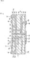
- a multilayer wiring board 10 includes alternately stacked basic material layers 30, 32, and 34 and constrained layers 40, 42, 44, and 46.
- Conductor patterns 16x, 16y, 16z, and 18 and conductor patterns 20 to 26 that extend in the surface direction of the basic material layers 30, 32, and 34 and the constrained layers 40, 42, 44, and 46 are formed on surfaces of the basic material layers 30, 32, and 34 or surfaces of the constrained layers 40, 42, 44, and 46.
- a conductor pattern (an intermediate conductor pattern) 17 is disposed inside the basic material layer 32.
- via-hole conductors 14a to 14h are connected to the conductor patterns 16x, 16y, 16z, 18, 20 and the conductor patterns 23 to 26.
- the via-hole conductors 14a to 14h extend in a direction in which the basic material layers 30, 32, and 34 and the constrained layers 40, 42, 44, and 46 are stacked.
- the via-hole conductor 14c is connected to the intermediate conductor pattern 17 disposed inside the basic material layer 32.
- An end of a via body 18 of the via-hole conductor 14c connected to the intermediate conductor pattern 17 is extended towards the constrained layer 44.
- an extended portion 15 that passes beyond the intermediate conductor pattern 17 and reaches the constrained layer 44 is formed.
- the basic material layer 32 By forming the extended portion 15 of the via-hole conductor 14c, the basic material layer 32 includes the via body 18 and the extended portion 15 of the via-hole conductor 14c disposed on either side of the intermediate conductor pattern 17. Accordingly, when being fired, contraction behaviors of two portions of the ceramic green sheet that forms the basic material layer 32 on either side of the intermediate conductor pattern 17 are substantially the same and, therefore, the difference between the contraction behaviors is decreased. Consequently, cracking occurring at a connection portion of the via-hole conductor 14c and the intermediate conductor pattern 17 can be prevented.
- the extended portion 15 is coaxial with the via body 18.
- the extended portion 15 and the via body 18 have the same diameter. If the extended portion 15 is formed so as to be coaxial with the via body 18, a contraction force can be evenly propagated to the both sides of the intermediate conductor pattern 17 when the ceramic green sheet is fired. Accordingly, the occurrence of cracking is further easily prevented.
- the extended portion 15 is formed so as to have a diameter the same as that of the via body 18, the difference between the contraction behaviors on either side of the intermediate conductor pattern 17 is negligible when the ceramic green sheet is fired. Accordingly, the occurrence of cracking is further easily prevented.
- an end surface 15x of the extended portion 15 is in contact with a surface 44a of the constrained layer 44 adjacent to the basic material layer 32 having the via-hole conductor 14c formed therein.
- the extended portion 15 of the via-hole conductor 14c is also supported by the constrained layer 44. Accordingly, contraction of the extended portion 15 in the surface direction can be constrained. Consequently, the occurrence of cracking starting from the extended portion 15 can be prevented. Since a surface of the basic material layer 32 having the via-hole conductor 14c formed therein and the end surface 15x of the extended portion 15 of the via-hole conductor 14c are coplanar, the structure of the constrained layer 44 can be simplified.
- the thickness of the basic material layer 32 having the intermediate conductor pattern 17 formed therein may be greater than the thickness of each of the other basic material layers 30 and 34.
- the thickness of the basic material layer having the intermediate conductor pattern 17 formed therein tends to be greater than the thickness of each of the other basic material layers 30 and 34 each being formed from a single ceramic green sheet group.
- chip electronic components 2 and 4 are joined, using solders 3 and 5, to the conductor patterns 20 to 23 exposed at a top surface 10a of the multilayer wiring board 10.
- an IC chip 6 is flip-chip bonded, using solder balls 7, to end surfaces of the via-hole conductors 14b to 14f exposed at the top surface 10a of the multilayer wiring board 10.
- An underfill resin 8 is filled between the IC chip 6 and the top surface 10a of the multilayer wiring board 10.
- the conductor patterns 24 and 25 exposed at a bottom surface 10b of the multilayer wiring board 10 are used as connection terminals that connect the multilayer wiring board 10 with another multilayer wiring board (not shown).
- Each of the basic material layers 30, 32, and 34 is formed by firing one or more ceramic green sheets including a first ceramic material.
- the basic material layers 30, 32, and 34 determine the board characteristic of the multilayer wiring board 10.
- Each of the constrained layers 40, 42, 44, and 46 is formed by firing one or more ceramic green sheets including a second ceramic material.
- each of the basic material layers 30, 32, and 34 range from 8 ⁇ m to 100 ⁇ m after the green sheets is sintered.
- the thickness of each of the basic material layers 30, 32, and 34 is not limited to that range. However, it is desirable that the thickness of each of the basic material layers 30, 32, and 34 be less than or equal to a maximum thickness of each of the constrained layers 40, 42, 44, and 46 that can be constrained during firing.
- the thicknesses of the basic material layers 30, 32, and 34 may differ from one another.
- a ceramic material part (e.g., a glass component) of which is impregnated in the constrained layers 40, 42, 44, and 46 during firing is used as the first ceramic material.
- the first ceramic material be a low-temperature co-fired ceramic (LTCC) that can be fired at a relatively low temperature, for example, a temperature lower than or equal to 1050°C.
- LTCC low-temperature co-fired ceramic
- glass ceramic that is a mixture of alumina and borosilicate-based glass or Ba-Al-Si-O-based ceramic that generates a glass component during firing can be used as the first ceramic material.
- the second ceramic material is adhered to part of the first ceramic material that interpenetrates from the basic material layers 30, 32, and 34. Accordingly, the constrained layers 40, 42, 44, and 46 are solidified. In addition, the basic material layers 30, 32, and 34 adjacent to the constrained layers 40, 42, 44, and 46 are joined.
- the constrained layers 40, 42, 44, and 46 include the unsintered second ceramic material having a sintering temperature higher than that of the first ceramic material. Accordingly, during firing, the constrained layers 40, 42, 44, and 46 restricts contraction thereof in the surface direction with respect to the basic material layers 30, 32, and 34. In addition, as noted above, the constrained layers 40, 42, 44, and 46 are adhered and joined when part of the first ceramic material interpenetrates.
- each of the constrained layers 40, 42, 44, and 46 be about 1 ⁇ m to about 10 ⁇ m after being sintered although, precisely speaking, the thickness depends on the states of the constrained layers 40, 42, 44, and 46, a desired force of constraint, and a firing condition.
- the material of conductor portions of the conductor patterns and the via-hole conductors can consist primarily of a conductive component that can be sintered at the same time as the basic material layers 30, 32, and 34 are sintered.
- a widely known material can be used as the material of conductor portions of the conductor patterns and the via-hole conductors. More specifically, Cu, Ag, Ni, Pd, an oxide thereof, or an alloy component thereof can be used.
- the conductor portions consisting primarily of Cu are formed.
- a method for manufacturing the multilayer wiring board 10 is described next.
- the following ceramic green sheet groups are prepared: a ceramic green sheet group 30x corresponding to the basic material layer 30 shown in Fig. 1 , ceramic green sheet groups 32s and 32t corresponding to the basic material layer 32 shown in Fig. 1 , a ceramic green sheet group 34x corresponding to the basic material layer 34 shown in Fig. 1 , and ceramic green sheet groups 40x, 42x, 44x, and 46x corresponding to the constrained layers 40, 42, 44, and 46 shown in Fig. 1 , respectively.
- the two ceramic green sheet groups 32s and 32t are prepared.
- a single ceramic green sheet group is prepared for each of the other layers.
- Each of the ceramic green sheet groups 30x, 32s, 32t, 34x, 40x, 42x, 44x, and 46x is formed by pressing a single ceramic green sheet or stacking and pressing a plurality of ceramic green sheets.
- one side of each of the ceramic green sheet groups 30x, 32s, 32t, 34x, 40x, 42x, 44x, and 46x is supported by a carrier film (not shown).
- a through-hole is formed in each of the ceramic green sheet groups 30x, 32s, 32t, 34x, 40x, 42x, 44x, and 46x by using, for example, a die. Thereafter, a conductive paste is filled with the through-holes.
- via-hole conductors 31a to 31g, via-hole conductors 33c to 33e, via-hole conductors 35c to 35e, via-hole conductors 37d and 37h, via-hole conductors 41a to 41g, via-hole conductors 43c to 43e, a via-hole conductor 45d, and via-hole conductors 47d and 47h are formed.
- conductive paste is printed on a surface of each of the ceramic green sheet groups 32t, 40x, 42x, 44x, and 46x so that a conductor pattern 33x, conductor patterns 41s to 41v, conductor patterns 43x to 43z, a conductor pattern 46x, and conductor patterns 47s and 47t are formed, respectively.
- the generated ceramic green sheet groups 30x, 32s, 32t, and 34x and the generated ceramic green sheet groups 40x, 42x, 44x, and 46x are stacked and pressed in predetermined orders and in predetermined directions.
- a ceramic green sheet compact is generated.
- the conductor pattern 33x serving as a wiring electrode is disposed between the ceramic green sheet groups 32s and 32t used for forming the basic material layer 32. If, for the conductor pattern 33x serving as the intermediate conductor pattern 17 (refer to Figs. 1 and 3 ), the via-hole conductor 33c to be connected to the conductor pattern 33x is provided in the ceramic green sheet group 32s, the via-hole conductor 33c extending to the neighboring ceramic green sheet group 44x is also provided in a portion located at a coaxial position when the ceramic green sheet group 32s is joined to the ceramic green sheet group 32t.
- the ceramic green sheets may be pressed in an appropriate order so that a ceramic green sheet compact is formed.
- the ceramic green sheet compact is fired in a predetermined atmosphere at a predetermined temperature.
- the multilayer wiring board 10 as shown in Fig. 3 is achieved.
- the basic material layers 30, 32, and 34 tend to contract.
- the constrained layers 40, 42, 44, and 46 act to constrain the contraction of the basic material layers 30, 32, and 34.
- the multilayer wiring board 10 having high precision dimensions can be manufactured.
- conductive paste used for the via-hole conductors 31a to 31g, the via-hole conductors 33c to 33e, the via-hole conductors 35c to 35e, the via-hole conductors 37d and 37h, the via-hole conductors 41a to 41g, the via-hole conductors 43c to 43e, the via-hole conductor 45d, and the via-hole conductors 47d and 47h may include glass of an amount that does not impair the conductivity and the surface treatment.
- the composition of the conductive paste is not limited to the above-described composition if the composition does not reduce the effect of the present invention.
- the firing atmosphere is appropriately changed in accordance with the type of the first ceramic material and the type of conductive particles contained in a conductive paste film.
- a Ba-Al-Si-O-based ceramic material was used for the first ceramic material of the basic material layers 30, 32, and 34.
- Alumina was used for the second ceramic material of the constrained layers 40, 42, 44, and 46.
- the thickness of each of the sintered basic material layers 30 and 34 was set to 20 ⁇ m.
- the thickness of the sintered basic material layer 32 was set to 40 ⁇ m.
- the thickness of each of the sintered constrained layers 40, 42, 44, and 46 was set to 3 ⁇ m. Note that the thickness of the basic material layer 32 may be the same as that of the basic material layers 30 and 34 if a desired electrical characteristic and mechanical strength can be obtained.
- TABLE 1 shows the cracking occurrence rates of the particular example and the comparative example. The number of samples is 100 for both examples. TABLE 1 Cracking Occurrence Rate Particular Example 0% Comparative Example 90%
- a multilayer wiring board according to a second embodiment is described next with reference to Fig. 5 .
- a multilayer wiring board has a structure substantially the same as that of the multilayer wiring board 10 of the first embodiment.
- different points are mainly described. The same numbering will be used in the following description as was utilized above in describing the first embodiment.
- the end surface 15x of an extended portion 15a of the via-hole conductor 14c is not in contact with the constrained layer 44. Instead, the end surface 15x passes through the constrained layer 44 and is in contact with a basic material layer 36 located on the other surface of the constrained layer 44.
- the occurrence of cracking in the intermediate conductor pattern 17 can be prevented.
- the occurrence of cracking starting from the extended portion 15a of the via-hole conductor 14c can be prevented.
- the reliability of the basic material layer 36 can be increased.
- a multilayer wiring board of a third embodiment has a structure similar to that of the first embodiment.
- an extended portion 15b of the via-hole conductor 14c extends to the middle point of the constrained layer 44.
- Such a structure can be generated by, for example, forming the constrained layer 44 using a plurality of green sheets and stacking the green sheet including a through-hole filled with a conductive material and the green sheet including no through-hole.
- the through-hole filled with a conductive material corresponds to the extended portion 15b of the via-hole conductor 14c.
- the occurrence of cracking in the intermediate conductor pattern 17 can be prevented.
- the occurrence of cracking starting from the extended portion 15b of the via-hole conductor 14c can be prevented.
- the reliability of the basic material layer 36 can be increased.
- the via-hole conductor 14c to be connected with the intermediate conductor pattern 17 disposed inside the basic material layer 32 is extended beyond the intermediate conductor pattern 17 so that the extended portion 15, 15a, 15b, or 15c is generated.
- the extended portions 15, 15a, 15b, and 15c do not have electrical conductivity.
- contraction behaviors of two portions of the ceramic green sheet that forms the basic material layer 32 on either side of the intermediate conductor pattern 17 can be made substantially the same and, therefore, cracking occurring at a connection portion of the intermediate conductor pattern and the via-hole conductor 14c and in the vicinity thereof can be prevented. As a result, the wiring efficiency of the multilayer wiring board can be increased.
Landscapes
- Engineering & Computer Science (AREA)
- Microelectronics & Electronic Packaging (AREA)
- Manufacturing & Machinery (AREA)
- Chemical & Material Sciences (AREA)
- Ceramic Engineering (AREA)
- Inorganic Chemistry (AREA)
- Production Of Multi-Layered Print Wiring Board (AREA)
- Structure Of Printed Boards (AREA)
Claims (4)
- Eine Mehrschichtverdrahtungsplatine, die folgende Merkmale aufweist:zumindest eine Grundmaterialschicht (30, 32, 34) einschließlich eines ersten Keramikmaterials und zumindest eine eingezwängte Schicht (40, 42, 44, 46) einschließlich eines zweiten Keramikmaterials, die abwechselnd gestapelt sind, wobei die eingezwängte Schicht (40, 42, 44, 46) eine Kontraktion derselben in einer Oberflächenrichtung in Bezug auf die Grundmaterialschicht (30, 32, 34) einschränkt;ein Leitermuster (16x-z, 19, 20-25), das auf der Grundmaterialschicht (30, 32, 34) oder der eingezwängten Schicht (40, 42, 44, 46) angeordnet ist, wobei sich das Leitermuster (16x-z, 19, 20-25) in der Oberflächenrichtung erstreckt, in der sich die Grundmaterialschicht (30, 32, 34) und die eingezwängte Schicht (40, 42, 44, 46) erstrecken;einen Durchgangslochleiter (14c), der sich in zumindest der Grundmaterialschicht (30, 32, 34) in einer Richtung erstreckt, in der die Grundmaterialschicht (30, 32, 34) und die eingezwängte Schicht (40, 42, 44, 46) gestapelt sind, wobei der Durchgangslochleiter (14c) mit dem Leitermuster (16x-z) verbunden ist; undein Zwischenleitermuster (17), das in der Grundmaterialschicht (30, 32, 34) angeordnet ist,wobei der Durchgangslochleiter (14c) mit dem Zwischenleitermuster (17) verbunden ist und einen Durchgangskörper (18) sowie einen erweiterten Abschnitt (15) umfasst, die jeweils auf einer der beiden Seiten des Zwischenleitermusters (17) angeordnet sind,wobei der Durchgangskörper (18) mit dem Zwischenleitermuster (17) verbunden ist,wobei der erweiterte Abschnitt (15) durch Erweitern des Durchgangskörpers (18) in einer Richtung zu der eingezwängten Schicht (40, 42, 44, 46) hin und von dem Durchgangskörper (18) weg gebildet ist, und ein erstes Ende des erweiterten Abschnittes (15) mit dem Zwischenleitermuster (17) verbunden ist, undwobei ein zweites Ende des erweiterten Abschnittes (15) des Durchgangslochleiters (14c) mit der eingezwängten Schicht (40, 42, 44, 46) in Kontakt steht,dadurch gekennzeichnet, dasseine Endoberfläche (15x) des erweiterten Abschnittes (15) mit einer Oberfläche (44a) der eingezwängten Schicht (44) in Kontakt steht, die zu der Grundmaterialschicht (32), in der der Durchgangslochleiter (14c) vorgesehen ist, benachbart ist.
- Die Mehrschichtverdrahtungsplatine gemäß Anspruch 1, bei der der erweiterte Abschnitt (15) des Durchgangslochleiters (14c) dahin gehend gebildet ist, mit dem Durchgangskörper (18) koaxial zu sein.
- Die Mehrschichtverdrahtungsplatine gemäß Anspruch 2, bei der der Durchmesser des erweiterten Abschnittes (15) des Durchgangslochleiters (14c) genauso groß ist wie der Durchmesser des Durchgangskörpers (18).
- Die Mehrschichtverdrahtungsplatine gemäß einem der Ansprüche 1 bis 3, bei der die Dicke der Grundmaterialschicht (32), in der das Zwischenleitermuster (17) vorliegt, größer ist als die Dicke der anderen Grundmaterialschichten (30, 34).
Applications Claiming Priority (2)
| Application Number | Priority Date | Filing Date | Title |
|---|---|---|---|
| JP2007052114 | 2007-03-01 | ||
| PCT/JP2008/052849 WO2008108172A1 (ja) | 2007-03-01 | 2008-02-20 | 多層配線基板 |
Publications (3)
| Publication Number | Publication Date |
|---|---|
| EP2129201A1 EP2129201A1 (de) | 2009-12-02 |
| EP2129201A4 EP2129201A4 (de) | 2010-12-22 |
| EP2129201B1 true EP2129201B1 (de) | 2017-04-12 |
Family
ID=39738069
Family Applications (1)
| Application Number | Title | Priority Date | Filing Date |
|---|---|---|---|
| EP08711655.4A Not-in-force EP2129201B1 (de) | 2007-03-01 | 2008-02-20 | Mehrschichtiges schaltungssubstrat |
Country Status (4)
| Country | Link |
|---|---|
| US (1) | US8541694B2 (de) |
| EP (1) | EP2129201B1 (de) |
| JP (1) | JP4905550B2 (de) |
| WO (1) | WO2008108172A1 (de) |
Families Citing this family (8)
| Publication number | Priority date | Publication date | Assignee | Title |
|---|---|---|---|---|
| KR101070022B1 (ko) * | 2009-09-16 | 2011-10-04 | 삼성전기주식회사 | 다층 세라믹 회로 기판, 다층 세라믹 회로 기판 제조방법 및 이를 이용한 전자 디바이스 모듈 |
| JP5835282B2 (ja) | 2013-07-04 | 2015-12-24 | 株式会社村田製作所 | 多層配線基板の製造方法およびプローブカードの製造方法並びに多層配線基板およびプローブカード |
| US9635761B2 (en) * | 2013-07-15 | 2017-04-25 | Massachusetts Institute Of Technology | Sleeved coaxial printed circuit board vias |
| US10249943B2 (en) | 2014-06-18 | 2019-04-02 | Massachusetts Institute Of Technology | Printed circuit board assembly with foam dielectric material |
| US10950929B2 (en) | 2016-07-14 | 2021-03-16 | Massachusetts Institute Of Technology | Foam radiator |
| WO2020129945A1 (ja) * | 2018-12-21 | 2020-06-25 | 株式会社村田製作所 | 積層体及び電子部品 |
| WO2020241775A1 (ja) * | 2019-05-29 | 2020-12-03 | 京セラ株式会社 | 電子素子実装用基板、電子装置、および電子モジュール |
| US12177964B2 (en) | 2021-01-21 | 2024-12-24 | Unimicron Technology Corp. | Circuit board and manufacturing method thereof and electronic device |
Family Cites Families (10)
| Publication number | Priority date | Publication date | Assignee | Title |
|---|---|---|---|---|
| US4487993A (en) * | 1981-04-01 | 1984-12-11 | General Electric Company | High density electronic circuits having very narrow conductors |
| JPS5852900A (ja) * | 1981-09-24 | 1983-03-29 | 株式会社日立製作所 | セラミツク多層配線板の製造方法 |
| FR2556503B1 (fr) * | 1983-12-08 | 1986-12-12 | Eurofarad | Substrat d'interconnexion en alumine pour composant electronique |
| US4910643A (en) * | 1988-06-06 | 1990-03-20 | General Electric Company | Thick film, multi-layer, ceramic interconnected circuit board |
| JP3656484B2 (ja) | 1999-03-03 | 2005-06-08 | 株式会社村田製作所 | セラミック多層基板の製造方法 |
| JP4201436B2 (ja) * | 1999-07-14 | 2008-12-24 | 日東電工株式会社 | 多層配線基板の製造方法 |
| JP2001160681A (ja) * | 1999-12-02 | 2001-06-12 | Murata Mfg Co Ltd | 多層セラミック基板およびその製造方法 |
| TW569424B (en) * | 2000-03-17 | 2004-01-01 | Matsushita Electric Industrial Co Ltd | Module with embedded electric elements and the manufacturing method thereof |
| JP4696443B2 (ja) * | 2003-09-19 | 2011-06-08 | 株式会社村田製作所 | 多層セラミック基板の製造方法 |
| JP4867276B2 (ja) * | 2005-10-14 | 2012-02-01 | 株式会社村田製作所 | セラミック基板の製造方法 |
-
2008
- 2008-02-20 WO PCT/JP2008/052849 patent/WO2008108172A1/ja not_active Ceased
- 2008-02-20 EP EP08711655.4A patent/EP2129201B1/de not_active Not-in-force
- 2008-02-20 JP JP2009502508A patent/JP4905550B2/ja not_active Expired - Fee Related
-
2009
- 2009-08-18 US US12/542,736 patent/US8541694B2/en not_active Expired - Fee Related
Non-Patent Citations (1)
| Title |
|---|
| None * |
Also Published As
| Publication number | Publication date |
|---|---|
| WO2008108172A1 (ja) | 2008-09-12 |
| JP4905550B2 (ja) | 2012-03-28 |
| JPWO2008108172A1 (ja) | 2010-06-10 |
| US20090294167A1 (en) | 2009-12-03 |
| EP2129201A4 (de) | 2010-12-22 |
| EP2129201A1 (de) | 2009-12-02 |
| US8541694B2 (en) | 2013-09-24 |
Similar Documents
| Publication | Publication Date | Title |
|---|---|---|
| EP2129201B1 (de) | Mehrschichtiges schaltungssubstrat | |
| JP4310467B2 (ja) | 複合多層基板及びその製造方法 | |
| US7362560B2 (en) | Multilayer electronic component and method for producing the same | |
| EP1921904B1 (de) | Keramische elektronische komponente und verfahren zur ihrer herstellung | |
| KR100853144B1 (ko) | 칩형 전자부품을 탑재한 세라믹 기판 및 그 제조방법 | |
| JP6128209B2 (ja) | 多層配線基板及びその製造方法並びにプローブカード用基板 | |
| JP2006128229A (ja) | 複合多層基板 | |
| JP3928665B2 (ja) | チップ型電子部品内蔵型多層基板及びその製造方法 | |
| JP3003413B2 (ja) | 多層セラミック基板の製造方法 | |
| JP2006032747A (ja) | 積層電子部品及びその製造方法 | |
| KR100956212B1 (ko) | 다층 세라믹 기판의 제조 방법 | |
| JP2007311596A (ja) | 突起電極付き回路基板の製造方法及び突起電極付き回路基板 | |
| JPH0155594B2 (de) | ||
| JP2000323806A (ja) | バンプ付セラミック回路基板及びその製造方法 | |
| JP2006032442A (ja) | 多層基板及びその製造方法 | |
| JP2006060148A (ja) | セラミック電子部品及びコンデンサ | |
| JP5598606B2 (ja) | 多層セラミック基板の製造方法 | |
| JP3909285B2 (ja) | 配線基板 | |
| JP2007067364A (ja) | チップ型電子部品を搭載したセラミック基板及びその製造方法 | |
| JP2009147160A (ja) | 多層セラミック基板の製造方法及び多層セラミック基板、これを用いた電子部品 | |
| KR100393592B1 (ko) | 도전성 페이스트 및 이를 이용한 집적 회로 장치 | |
| JP2000138309A (ja) | 導体ペースト、並びに、セラミック多層基板及びその製造方法 | |
| JP2006135110A (ja) | セラミック多層基板及びその製造方法 | |
| JPH0645762A (ja) | 多層セラミック基板とその製造方法 | |
| JP2003133740A (ja) | 多層回路基板 |
Legal Events
| Date | Code | Title | Description |
|---|---|---|---|
| PUAI | Public reference made under article 153(3) epc to a published international application that has entered the european phase |
Free format text: ORIGINAL CODE: 0009012 |
|
| 17P | Request for examination filed |
Effective date: 20090727 |
|
| AK | Designated contracting states |
Kind code of ref document: A1 Designated state(s): AT BE BG CH CY CZ DE DK EE ES FI FR GB GR HR HU IE IS IT LI LT LU LV MC MT NL NO PL PT RO SE SI SK TR |
|
| DAX | Request for extension of the european patent (deleted) | ||
| A4 | Supplementary search report drawn up and despatched |
Effective date: 20101123 |
|
| 17Q | First examination report despatched |
Effective date: 20140314 |
|
| GRAP | Despatch of communication of intention to grant a patent |
Free format text: ORIGINAL CODE: EPIDOSNIGR1 |
|
| INTG | Intention to grant announced |
Effective date: 20161025 |
|
| GRAS | Grant fee paid |
Free format text: ORIGINAL CODE: EPIDOSNIGR3 |
|
| GRAA | (expected) grant |
Free format text: ORIGINAL CODE: 0009210 |
|
| AK | Designated contracting states |
Kind code of ref document: B1 Designated state(s): AT BE BG CH CY CZ DE DK EE ES FI FR GB GR HR HU IE IS IT LI LT LU LV MC MT NL NO PL PT RO SE SI SK TR |
|
| REG | Reference to a national code |
Ref country code: GB Ref legal event code: FG4D |
|
| REG | Reference to a national code |
Ref country code: CH Ref legal event code: EP |
|
| REG | Reference to a national code |
Ref country code: IE Ref legal event code: FG4D |
|
| REG | Reference to a national code |
Ref country code: AT Ref legal event code: REF Ref document number: 884978 Country of ref document: AT Kind code of ref document: T Effective date: 20170515 |
|
| REG | Reference to a national code |
Ref country code: DE Ref legal event code: R096 Ref document number: 602008049708 Country of ref document: DE |
|
| REG | Reference to a national code |
Ref country code: NL Ref legal event code: MP Effective date: 20170412 |
|
| REG | Reference to a national code |
Ref country code: LT Ref legal event code: MG4D |
|
| REG | Reference to a national code |
Ref country code: AT Ref legal event code: MK05 Ref document number: 884978 Country of ref document: AT Kind code of ref document: T Effective date: 20170412 |
|
| PG25 | Lapsed in a contracting state [announced via postgrant information from national office to epo] |
Ref country code: NL Free format text: LAPSE BECAUSE OF FAILURE TO SUBMIT A TRANSLATION OF THE DESCRIPTION OR TO PAY THE FEE WITHIN THE PRESCRIBED TIME-LIMIT Effective date: 20170412 |
|
| PG25 | Lapsed in a contracting state [announced via postgrant information from national office to epo] |
Ref country code: GR Free format text: LAPSE BECAUSE OF FAILURE TO SUBMIT A TRANSLATION OF THE DESCRIPTION OR TO PAY THE FEE WITHIN THE PRESCRIBED TIME-LIMIT Effective date: 20170713 Ref country code: HR Free format text: LAPSE BECAUSE OF FAILURE TO SUBMIT A TRANSLATION OF THE DESCRIPTION OR TO PAY THE FEE WITHIN THE PRESCRIBED TIME-LIMIT Effective date: 20170412 Ref country code: NO Free format text: LAPSE BECAUSE OF FAILURE TO SUBMIT A TRANSLATION OF THE DESCRIPTION OR TO PAY THE FEE WITHIN THE PRESCRIBED TIME-LIMIT Effective date: 20170712 Ref country code: LT Free format text: LAPSE BECAUSE OF FAILURE TO SUBMIT A TRANSLATION OF THE DESCRIPTION OR TO PAY THE FEE WITHIN THE PRESCRIBED TIME-LIMIT Effective date: 20170412 Ref country code: ES Free format text: LAPSE BECAUSE OF FAILURE TO SUBMIT A TRANSLATION OF THE DESCRIPTION OR TO PAY THE FEE WITHIN THE PRESCRIBED TIME-LIMIT Effective date: 20170412 Ref country code: FI Free format text: LAPSE BECAUSE OF FAILURE TO SUBMIT A TRANSLATION OF THE DESCRIPTION OR TO PAY THE FEE WITHIN THE PRESCRIBED TIME-LIMIT Effective date: 20170412 Ref country code: AT Free format text: LAPSE BECAUSE OF FAILURE TO SUBMIT A TRANSLATION OF THE DESCRIPTION OR TO PAY THE FEE WITHIN THE PRESCRIBED TIME-LIMIT Effective date: 20170412 |
|
| PG25 | Lapsed in a contracting state [announced via postgrant information from national office to epo] |
Ref country code: PL Free format text: LAPSE BECAUSE OF FAILURE TO SUBMIT A TRANSLATION OF THE DESCRIPTION OR TO PAY THE FEE WITHIN THE PRESCRIBED TIME-LIMIT Effective date: 20170412 Ref country code: SE Free format text: LAPSE BECAUSE OF FAILURE TO SUBMIT A TRANSLATION OF THE DESCRIPTION OR TO PAY THE FEE WITHIN THE PRESCRIBED TIME-LIMIT Effective date: 20170412 Ref country code: LV Free format text: LAPSE BECAUSE OF FAILURE TO SUBMIT A TRANSLATION OF THE DESCRIPTION OR TO PAY THE FEE WITHIN THE PRESCRIBED TIME-LIMIT Effective date: 20170412 Ref country code: BG Free format text: LAPSE BECAUSE OF FAILURE TO SUBMIT A TRANSLATION OF THE DESCRIPTION OR TO PAY THE FEE WITHIN THE PRESCRIBED TIME-LIMIT Effective date: 20170712 Ref country code: IS Free format text: LAPSE BECAUSE OF FAILURE TO SUBMIT A TRANSLATION OF THE DESCRIPTION OR TO PAY THE FEE WITHIN THE PRESCRIBED TIME-LIMIT Effective date: 20170812 |
|
| REG | Reference to a national code |
Ref country code: DE Ref legal event code: R097 Ref document number: 602008049708 Country of ref document: DE |
|
| PG25 | Lapsed in a contracting state [announced via postgrant information from national office to epo] |
Ref country code: RO Free format text: LAPSE BECAUSE OF FAILURE TO SUBMIT A TRANSLATION OF THE DESCRIPTION OR TO PAY THE FEE WITHIN THE PRESCRIBED TIME-LIMIT Effective date: 20170412 Ref country code: DK Free format text: LAPSE BECAUSE OF FAILURE TO SUBMIT A TRANSLATION OF THE DESCRIPTION OR TO PAY THE FEE WITHIN THE PRESCRIBED TIME-LIMIT Effective date: 20170412 Ref country code: SK Free format text: LAPSE BECAUSE OF FAILURE TO SUBMIT A TRANSLATION OF THE DESCRIPTION OR TO PAY THE FEE WITHIN THE PRESCRIBED TIME-LIMIT Effective date: 20170412 Ref country code: EE Free format text: LAPSE BECAUSE OF FAILURE TO SUBMIT A TRANSLATION OF THE DESCRIPTION OR TO PAY THE FEE WITHIN THE PRESCRIBED TIME-LIMIT Effective date: 20170412 Ref country code: CZ Free format text: LAPSE BECAUSE OF FAILURE TO SUBMIT A TRANSLATION OF THE DESCRIPTION OR TO PAY THE FEE WITHIN THE PRESCRIBED TIME-LIMIT Effective date: 20170412 |
|
| PLBE | No opposition filed within time limit |
Free format text: ORIGINAL CODE: 0009261 |
|
| STAA | Information on the status of an ep patent application or granted ep patent |
Free format text: STATUS: NO OPPOSITION FILED WITHIN TIME LIMIT |
|
| PG25 | Lapsed in a contracting state [announced via postgrant information from national office to epo] |
Ref country code: IT Free format text: LAPSE BECAUSE OF FAILURE TO SUBMIT A TRANSLATION OF THE DESCRIPTION OR TO PAY THE FEE WITHIN THE PRESCRIBED TIME-LIMIT Effective date: 20170412 |
|
| 26N | No opposition filed |
Effective date: 20180115 |
|
| PG25 | Lapsed in a contracting state [announced via postgrant information from national office to epo] |
Ref country code: SI Free format text: LAPSE BECAUSE OF FAILURE TO SUBMIT A TRANSLATION OF THE DESCRIPTION OR TO PAY THE FEE WITHIN THE PRESCRIBED TIME-LIMIT Effective date: 20170412 |
|
| REG | Reference to a national code |
Ref country code: CH Ref legal event code: PL |
|
| PG25 | Lapsed in a contracting state [announced via postgrant information from national office to epo] |
Ref country code: MC Free format text: LAPSE BECAUSE OF FAILURE TO SUBMIT A TRANSLATION OF THE DESCRIPTION OR TO PAY THE FEE WITHIN THE PRESCRIBED TIME-LIMIT Effective date: 20170412 |
|
| GBPC | Gb: european patent ceased through non-payment of renewal fee |
Effective date: 20180220 |
|
| REG | Reference to a national code |
Ref country code: IE Ref legal event code: MM4A |
|
| REG | Reference to a national code |
Ref country code: BE Ref legal event code: MM Effective date: 20180228 |
|
| PG25 | Lapsed in a contracting state [announced via postgrant information from national office to epo] |
Ref country code: CH Free format text: LAPSE BECAUSE OF NON-PAYMENT OF DUE FEES Effective date: 20180228 Ref country code: LU Free format text: LAPSE BECAUSE OF NON-PAYMENT OF DUE FEES Effective date: 20180220 Ref country code: LI Free format text: LAPSE BECAUSE OF NON-PAYMENT OF DUE FEES Effective date: 20180228 |
|
| REG | Reference to a national code |
Ref country code: FR Ref legal event code: ST Effective date: 20181031 |
|
| PG25 | Lapsed in a contracting state [announced via postgrant information from national office to epo] |
Ref country code: IE Free format text: LAPSE BECAUSE OF NON-PAYMENT OF DUE FEES Effective date: 20180220 |
|
| PG25 | Lapsed in a contracting state [announced via postgrant information from national office to epo] |
Ref country code: GB Free format text: LAPSE BECAUSE OF NON-PAYMENT OF DUE FEES Effective date: 20180220 Ref country code: BE Free format text: LAPSE BECAUSE OF NON-PAYMENT OF DUE FEES Effective date: 20180228 Ref country code: FR Free format text: LAPSE BECAUSE OF NON-PAYMENT OF DUE FEES Effective date: 20180228 |
|
| PG25 | Lapsed in a contracting state [announced via postgrant information from national office to epo] |
Ref country code: MT Free format text: LAPSE BECAUSE OF NON-PAYMENT OF DUE FEES Effective date: 20180220 |
|
| PG25 | Lapsed in a contracting state [announced via postgrant information from national office to epo] |
Ref country code: TR Free format text: LAPSE BECAUSE OF FAILURE TO SUBMIT A TRANSLATION OF THE DESCRIPTION OR TO PAY THE FEE WITHIN THE PRESCRIBED TIME-LIMIT Effective date: 20170412 |
|
| PG25 | Lapsed in a contracting state [announced via postgrant information from national office to epo] |
Ref country code: HU Free format text: LAPSE BECAUSE OF FAILURE TO SUBMIT A TRANSLATION OF THE DESCRIPTION OR TO PAY THE FEE WITHIN THE PRESCRIBED TIME-LIMIT; INVALID AB INITIO Effective date: 20080220 Ref country code: PT Free format text: LAPSE BECAUSE OF FAILURE TO SUBMIT A TRANSLATION OF THE DESCRIPTION OR TO PAY THE FEE WITHIN THE PRESCRIBED TIME-LIMIT Effective date: 20170412 |
|
| PG25 | Lapsed in a contracting state [announced via postgrant information from national office to epo] |
Ref country code: CY Free format text: LAPSE BECAUSE OF FAILURE TO SUBMIT A TRANSLATION OF THE DESCRIPTION OR TO PAY THE FEE WITHIN THE PRESCRIBED TIME-LIMIT Effective date: 20170412 |
|
| PGFP | Annual fee paid to national office [announced via postgrant information from national office to epo] |
Ref country code: DE Payment date: 20240219 Year of fee payment: 17 |
|
| REG | Reference to a national code |
Ref country code: DE Ref legal event code: R119 Ref document number: 602008049708 Country of ref document: DE |
|
| PG25 | Lapsed in a contracting state [announced via postgrant information from national office to epo] |
Ref country code: DE Free format text: LAPSE BECAUSE OF NON-PAYMENT OF DUE FEES Effective date: 20250902 |