EP2133797A1 - Dma-transfereinrichtung und verfahren - Google Patents
Dma-transfereinrichtung und verfahren Download PDFInfo
- Publication number
- EP2133797A1 EP2133797A1 EP08712081A EP08712081A EP2133797A1 EP 2133797 A1 EP2133797 A1 EP 2133797A1 EP 08712081 A EP08712081 A EP 08712081A EP 08712081 A EP08712081 A EP 08712081A EP 2133797 A1 EP2133797 A1 EP 2133797A1
- Authority
- EP
- European Patent Office
- Prior art keywords
- data
- transfer
- predetermined pattern
- dma
- memory
- Prior art date
- Legal status (The legal status is an assumption and is not a legal conclusion. Google has not performed a legal analysis and makes no representation as to the accuracy of the status listed.)
- Granted
Links
Images





Classifications
-
- G—PHYSICS
- G06—COMPUTING OR CALCULATING; COUNTING
- G06F—ELECTRIC DIGITAL DATA PROCESSING
- G06F13/00—Interconnection of, or transfer of information or other signals between, memories, input/output devices or central processing units
- G06F13/14—Handling requests for interconnection or transfer
- G06F13/20—Handling requests for interconnection or transfer for access to input/output bus
- G06F13/28—Handling requests for interconnection or transfer for access to input/output bus using burst mode transfer, e.g. direct memory access DMA, cycle steal
Definitions
- the present invention relates to an inter-memory data transfer apparatus and particularly, to a DMA (Direct Memory Access) transfer apparatus and a DMA transfer method.
- DMA Direct Memory Access
- This application is based upon and claims the benefit of priority from prior Japanese Patent Application No. 2007-049976 filed on February 28, 2007 .
- the entire contents of Japanese Patent Application No. 2007-049976 are incorporated in contents of the description of the present application.
- FIG. 10 is a view showing a configuration of a DMA transfer apparatus which is a background technique of the present invention.
- a DMA controller 107 for controlling DMA transfer includes a parameter register 101, a DMA control section 100, and IF 106.
- an external shared memory 102, an internal memory 103, a calculation core 108, and a CPU 109 are arranged around the DMA controller 107.
- the DMA controller 107, external shared memory 102, and CPU 109 are connected to data buses 110 and 111.
- the CPU 109 does not directly control data transfer from the external shared memory 102 to internal memory 103. That is, as shown in FIG. 10 , parameters such as a memory address offset, data number, and the like are set in the DMA controller 107 so as to allow the DMA controller 107 to control the data transfer. By performing the DMA transfer, a load of the CPU 109 can be reduced.
- Patent Document 1 JP-A-2001-154846
- Patent Document 2 JP-A-2006-155490
- Patent Document 3 JP-A-05-244167
- Patent Document 4 JP-A-05-336380
- Patent Document 5 JP-A-10-040399
- the abovementioned DMA transfer has the following three problems.
- the system shown in FIG. 10 has an external shared memory.
- the system When performing calculation, the system appropriately transfers data from the external memory to internal memory.
- a calculation unit is a systolic array, the simpler a data flow is, the more efficient calculation can be performed.
- the predetermined pattern data is transferred also in the DMA transfer time, causing a redundant transfer.
- a method of adding a function for generating the predetermined pattern in the calculation core so as to improve data transfer rate In this case, however, it is necessary to change a processing flow depending on whether the predetermined pattern data is handled or not, complicating the system configuration.
- An exemplary object of the present invention is to provide a DMA transfer apparatus and a DMA transfer method capable of reducing traffic on a bus between an external shared memory and DMA controller with less additional hardware to effectively use a memory.
- a DMA transfer apparatus that performs DMA transfer between memories, which includes:
- the pattern generation section for generating the predetermined pattern data in the DMA, transfer apparatus by adding the pattern generation section for generating the predetermined pattern data in the DMA, transfer apparatus, it is possible to reduce the amount of data transferred on a bus connecting a memory of the DMA transfer apparatus and a DMA transfer source memory, thereby improving use efficiency of the DMA transfer source memory.
- the predetermined pattern data are previously stored in the DMA transfer destination memory, so that an operation flow can be simplified. That is, it is not necessary to put the predetermined pattern data on the bus connecting the DMA transfer source memory and DMA transfer apparatus, simplifying the system configuration.
- the bus can be utilized also for data transfer between the DMA transfer source memory and another unit, thereby improving performance of the entire system. This is achieved also because of the elimination of the need of storing the predetermined pattern data in the DMA transfer source memory.
- a certain area of the DMA transfer destination memory can be reset by only the processing in the DMA transfer apparatus, without intervention of the CPU.
- Exemplary embodiments of the present invention assume a system that uses DMA transfer to performs data transfer from an external shared memory to an internal memory and handles large volume of data in an internal calculation core for, e.g., performing matrix calculation.
- data of a predetermined pattern such as a zero matrix or unit matrix is often handled.
- the data of a predetermined pattern such as a zero matrix or unit matrix is temporarily stored in an internal memory or external memory as in the case of other calculation data and transferred to a calculation core according to need (however, in the case where the predetermined pattern data is temporarily stored in the internal memory, since the internal memory is limited in capacity, the predetermined pattern data is overwritten by other data when it is not used in the subsequent calculation).
- the DMA transfer described as the background technique performs inter-memory data transfer based on the number of data or address offset set as a parameter.
- a zero matrix or unit matrix is required to be calculated using the same calculation path as that used by ordinary calculation data, it is necessary to include the zero matrix or unit matrix in the data to be subjected to inter-memory transfer by the DMA controller.
- the preferred embodiments aim to generate the predetermined pattern in the DMA controller and add the predetermined pattern data to transfer data from the external share memory so as to reduce the amount of data transferred on a bus connecting the DMA controller and external shared memory and improve use efficiency of the external share memory. Further, the preferred embodiments aim to eliminate the need of putting the predetermined pattern data on the bus connecting the external shared memory and DMA controller at the time of DMA transfer so as to simplify the system configuration.
- a pattern generation section is provided in the DMA controller and generates data of a predetermined pattern, such as a zero matrix or unit matrix, in the DMA controller when data is transferred from one memory to another memory. Further, transfer data read out from the one memory is temporarily held in a queuing section for queuing. At this time, switching between the transfer data from the queuing section and predetermined pattern data is made based on the number of the transfer data. The predetermined pattern data is added to a data stream to be transferred in this manner and the resultant data stream is transferred to the memory.
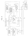
- FIG. 1 is a block diagram showing a system including a first embodiment of a DMA transfer apparatus according to the present invention.
- a DMA controller 17 serving as the DMA transfer apparatus is connected between an internal memory 15 and an external shared memory 14.
- the DMA controller 17 performs data transfer between memories (internal memory 15 and external shared memory 14).
- the DMA controller 17 includes a DMA control section 10 that controls DMA transfer, a pattern generation section 11 that generates predetermined pattern data, and a parameter register 12 that stores parameters used for the pattern generation.
- the predetermined pattern generated by the pattern generation section 11 is predetermined pattern data such as a zero matrix or unit matrix.
- the pattern generation section 11 generates the predetermined pattern based on parameters stored in the parameter register 12, such as a pattern index, added data size, insertion offset or insertion timing, and the like.
- the DMA controller 17 further includes a queuing unit 13, a multiplexer 25, and a memory data IF 16.
- the queuing unit 13 synchronizes the output timing of data transferred from the external shared memory 14 with output timing of predetermined pattern data output from the pattern generation section 11.
- the multiplexer 25 selectively outputs the transfer data from the queuing unit 13 and predetermined pattern from the pattern generation section 11 to the internal memory 15.
- the memory data IF 16 is connected to the internal memory 15 and queuing unit 13.
- the internal memory 15, external shared memory 14, calculation core 18, and a CPU 19 are arranged around the DMA controller 17.
- a data bus 20 and an address bus 21 connect the DMA controller 17, CPU 19, and external shared memory 14.
- the external shared memory 14 is a memory set as a transfer source or destination of the DMA transfer.
- the calculation core 18 performs matrix calculation using DMA-transfer data.
- the CPU 19 issues a command to the DMA controller 17.
- the DMA transfer of the DMA controller 17 is controlled by the command from the CPU 19 connected to the data bus 20 connecting the external shared memory 14 and DMA controller 17.
- FIG. 2 shows an example of configurations of the pattern generation section 11 and parameter register 12.
- the parameters stored in the parameter register 12 will first be described.
- the pattern index is a parameter for determining which pattern is to be output
- added data size is a parameter indicating the size of a predetermined pattern to be inserted.
- the insertion offset is a parameter indicating the timing at which the predetermined pattern is inserted into the transfer data for the first time.
- the insertion timing is a parameter indicating the insertion interval of the predetermined pattern in the case where the insertion of the predetermined pattern is performed a plurality of times.
- the data to be output to the internal memory 15 is switched from the transfer data to predetermined pattern.
- the parameters stored in the parameter register 12 are set by the CPU 19.
- the pattern generation section 11 includes a counter 23 and a pattern generation unit 26.
- the pattern generation unit 26 has an index decoder 22 and a selector 24.
- the index decoder 22 generates, as a control signal, timing for generating a unit matrix, zero matrix, or the like, based on the pattern index, etc., stored in the parameter register 12 and outputs it to the selector 24.
- the selector 24 selects 0 or in accordance with the control signal from the index decoder 22 and generates the predetermined pattern data such as a zero matrix or unit matrix.
- the counter 23 counts the number of transfer data from the external shared memory 14. The value counted by the counter 23 is used to determine the data size of the transfer data, and the timing at which the data to be output to the internal memory 15 is switched from the transfer data to predetermined pattern data is adjusted.
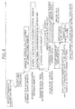
- FIG. 3 is a timing chart of the DMA transfer according to the present embodiment. In the following operation, the DMA transfer is assumed to be conducted from the external shared memory 14 to internal memory 15.
- the DMA controller 17 receives, from the CPU 19, a DMA transfer command, a data size, a beginning address, and parameters required for pattern generation, such as the pattern index, added data size, and insertion offset or insertion timing and starts DMA transfer.
- the parameters required for pattern generation is set in the parameter register 12 by the CPU 19,
- the DMA controller 17 then generates an address for accessing the external shared memory, starts accessing the external shared memory 14, and reads out, from the external shared memory 14, data at a specified address area by an amount corresponding to a specified data size.
- the counter 23 starts counting the number of the transfer data.
- the data read out from the external shared memory 14 is once transferred to the queuing unit 13 in the DMA controller 17 through the IF 16.
- the DMA controller 17 In synchronization with input of data into the queuing unit 13, the DMA controller 17 generates an address for accessing the internal memory as shown in FIG. 3 and outputs it to the internal memory 15 together with the transfer data input to the queuing unit 13.
- the queuing unit 13 is organized as a FIFO (First-In First-Out) and can output both data and address at one clock cycle if data insertion is not made.
- FIFO First-In First-Out
- the predetermined pattern data transferred from the pattern generation section 11 is selected by the multiplexer 25 and output to the internal memory 15.
- the pattern generation section 11 When the predetermined pattern is generated in the pattern generation section 11, "0" or "1" is selected by the selector 24 in accordance with the pattern index for determining which predetermined pattern is to be output which is set as a parameter in the parameter register 12 as described above, and thereby the predetermined pattern data such as a zero matrix or unit matrix is generated. At this time, the pattern generation section 11 generates the predetermined pattern data in accordance witch the added data size indicating the size of the predetermined pattern which is set in the parameter register 12 as described above.
- the same operation as described above is performed.
- data to be output is switched from the transfer data to predetermined pattern data in accordance with the insertion timing indicating the insertion interval of the predetermined pattern which is set in the parameter register 12 so that the predetermined pattern is inserted into the transfer data at constant intervals.
- the predetermined pattern is added to a data stream transferred from the external shared memory 14 in this manner, and the resultant data stream is transferred to the internal memory 15.
- the data value output from the pattern generation section 11 is set to a value of 0 or 1 in the present embodiment, the value is not limited to this.
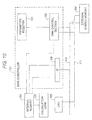
- FIG. 4 is a block diagram showing a system including a second embodiment of the DMA transfer apparatus according to the present invention.
- the same reference numerals as those in FIG. 1 denote the same parts as those in FIG. 1 .
- the second embodiment differs from the first embodiment in the point that the data output from the queuing unit 13 is used as a parameter in the pattern generation section 11 and in the configuration of the pattern generation section 11. Except for the above points, the configuration of the second embodiment is the same as that of the first embodiment shown in FIG. 1 .
- data transferred from the pattern generation section 11 and a value of the parameter index are used to select one of arbitrary two data stored in the parameter register 12 to generate the predetermined pattern.
- the DMA transfer in the present embodiment can be used in a case where a pattern to be inserted is changed depending on the type of data like a packet header.
- the DMA controller 17 includes the DMA control section 10, pattern generation section 11, parameter register 12, queuing unit 13, multiplexer 25, and memory data IF 16.
- the DMA control section 10 controls DMA transfer.
- the pattern generation section 11 generates a predetermined pattern.
- the parameter register 12 stores parameters used for pattern generation.
- the queuing unit 13 synchronizes the output timing of data transferred from the external shared memory 14 with output timing of predetermined pattern output from the pattern generation section 11.
- the multiplexer 25 selectively outputs the transfer data from the queuing unit 13 and predetermined pattern from the pattern generation section 11 to the internal memory 15.
- the memory data IF 16 is connected to the internal memory 15 and queuing unit 13.
- the internal memory 15, external shared memory 14, calculation core 18, and CPU 19 are arranged around the DMA controller 17.
- the data bus 20 and address bus 21 connect the DMA controller 17, CPU 19, and external shared memory 14.
- the external shared memory 14 is a memory set as a transfer source or destination of the DMA transfer.
- the internal memory 15 is a memory set as a transfer source or destination of the DMA transfer.
- the DMA transfer of the DMA controller 17 is controlled by a command from the CPU 19 connected to the data bus 20 connecting the external shared memory 14 and DMA controller 17.
- FIG. 5 shows configurations of the pattern generation section 11 and parameter register 12.
- the added data size, insertion offset, and insertion timing are the same as those described in FIG. 2 .
- arbitrary numbers 1 and 2 are set in the parameter register 12.
- the pattern generation unit 26 has the index decoder 22 and selector 24.
- the index decoder 22 generates, as a control signal, timing for generating the predetermined pattern based on the parameters stored in the parameter register 12.
- control signal and transfer data are input as parameters to the selector 24, and the selector 24 selects the arbitrary number 1 or 2 in accordance with the control signal and transfer data and outputs the selected arbitrary number as the predetermined pattern.
- the counter 23 counts the number of transfer data from the external shared memory 14. The value counted by the counter 23 is used to determine the data size of the transfer data, and the timing at which the predetermined pattern is inserted is adjusted.
- FIG. 6 is a timing chart of the DMA transfer according to the present embodiment. In the following operation, the DMA transfer is assumed to be conducted from the external shared memory 14 to internal memory 15.
- the DMA transfer operation according to the present embodiment is basically the same as that of the first embodiment shown in FIG. 3 but differs in that the predetermined pattern is generated by selecting the arbitrary number 1 or 2 in the selector 24, that is, the predetermined pattern generated in the pattern generation section 11 differs depending on the type of data.
- the DMA controller 17 receives, from the outside CPU 19, a DMA transfer command, a data size, a beginning address, and parameters required for pattern generation, such as the pattern index and added data size and starts DMA transfer.
- the DMA controller 17 then generates an address for accessing the external shared memory, starts accessing the external shared memory 14, and reads out, from the external shared memory 14, data at a specified address area by an amount corresponding to a specified data size.
- the counter 23 starts counting the number of the transfer data.
- the data read out from the external shared memory 14 is once transferred to the queuing unit 13 in the DMA controller 17.
- the DMA controller 17 In synchronization with input of data into the queuing unit 13, the DMA controller 17 generates an address for accessing the internal memory as shown in FIG. 6 and outputs it to the internal memory 15 together with the transfer data input to the queuing unit 13.
- the queuing unit 13 is organized as a FIFO and can output both data and address at one clock cycle if data insertion is not made.
- a parameter insertion offset stored in the parameter register 12 shown in FIG. 5
- data to be output is switched to the predetermined pattern data transferred from the pattern generation section 11, and the predetermined pattern is output to the internal memory 15.
- the arbitrary number 1 or 2 specified as the predetermined pattern is to be output is selected depending on the data transferred from the external shared memory 14. For example, when the transfer data is "1", the arbitrary number 1 is selected; and when the transfer data is "0", the arbitrary number 2 is selected. Then, the number of the arbitrary number 1 or 2 is selected based on the pattern index to thereby generate the predetermined pattern data.
- the pattern generation section 11 generates the predetermined pattern data in accordance with the added data size indicating the size of the predetermined pattern which is set in the parameter register 12.
- the same operation as above is performed.
- data to be output is switched from the transfer data to predetermined pattern in accordance with the insertion timing indicating the insertion interval of the predetermined pattern which is set in the parameter register 12 so that the predetermined pattern is inserted into the transfer data at constant intervals.
- the predetermined pattern is added to a data stream transferred from the external shared memory 14 in this manner, and the resultant data stream is transferred to the internal memory 15.
- the third embodiment is a modification of the second embodiment and differs from the second embodiment in the configuration of the pattern generation section 11 and predetermined pattern insertion process. Except for the above points, the configuration of the third embodiment is the same as that of the second embodiment shown in FIG. 4 .
- FIG. 7 shows a configuration of the pattern generation section 11 according to the present embodiment.
- the same reference numerals as those in FIG. 5 of the second embodiment denote the same parts as those in FIG. 5 .
- the pattern index and added data size of parameter register 22 are the same as those described in FIG. 2 .
- a trigger value is a parameter for switching between the transfer data and predetermine pattern.
- the index decoder 22 outputs, as a control signal, timing for selecting a predetermined pattern to be inserted based on the trigger value and transfer data from the queuing unit 13, to the selector 24.
- the selector 24 selects 0 or 1 stored in the parameter register 12 based on the control signal from the index decoder 22 and outputs it as the predetermined pattern.
- the present embodiment can be used in a case where the predetermined pattern generated in the pattern generation section 11 is DMA-transferred when the DMA transfer data from the external shared memory 14 represents a certain value (this value is assumed to previously be stored in the parameter register 12).
- FIG. 8 is a timing chart of the DMA transfer according to the present embodiment.
- the DMA transfer operation according to the present embodiment is basically the same as that of the second embodiment shown in FIG. 6 but differs in that the transfer data from the external shared memory 14 is used for switching between the transfer data from the external shared memory 14 and predetermined pattern. Except for the above point, the operation of the third embodiment is the same as that of the second embodiment.
- the DMA controller 17 receives a DMA transfer command from the CPU 19 and starts DMA transfer. Then the counter 23 starts counting operation, an address for accessing the external shared memory is generated by the DMA controller 17, and data is red out from the external shared memory 14.
- the data read out is once transferred to the queuing unit 13 in the DMA controller 17.
- the DMA controller 17 In synchronization with input of data into the queuing unit 13, the DMA controller 17 generates an address for accessing the internal memory and outputs it to the internal memory 15 together with the transfer data input to the queuing unit 13.
- the transfer data of the external shared memory 14 transferred from the queuing unit 13 and trigger value specified by the parameter are compared during the DMA transfer.
- data to be output is switched from the transfer data to predetermined pattern. For example, when all 1s of 32-bit data in the transfer data coincide with all 1s of 32-bit data of the trigger value, data to be output is switched from the transfer data to predetermined pattern.
- the transfer data from the external shared memory 14 held in the queuing unit 13 is output to the internal memory 13.
- the transfer data from the external shared memory 14 is held in the queuing unit 13.
- the data to be output is switched, and the transfer data held in the queuing unit 13 is output to the internal memory 15.
- the same operation as above is repeated to add the predetermined pattern data generated in the pattern generation section 11 to a data stream transferred from the external shared memory 14 and transfer the resultant data stream to the internal memory 15.
- the fourth embodiment is a modification of the first embodiment and differs from the first embodiment in the following point. That is, the timing of inserting the predetermined pattern used in the pattern generation section 11 that generates the predetermined pattern is specified using the number of data in the first embodiment; while in the fourth embodiment, the timing is specified using time (clock cycle) required from the start of the DMA transfer. Except for the above point, the configuration of the fourth embodiment is the same as that of the first embodiment.
- the fourth embodiment differs from the first embodiment in the operation of the pattern generation section 11. That is, at the time point when the DMA controller 17 receives a DMA command and the like from the CPU 19, the counter 23 starts counting operation and outputs the number of cycles required for the DMA transfer. The value output from the counter 23 is compared with a parameter indicating the DMA transfer timing which is set in the parameter register 12. When the value output from the counter 23 reaches the specified timing, the predetermined pattern generated in the pattern generation section 11 is DMA-transferred.
- FIG. 9 is a timing chart of the DMA transfer according to the present embodiment.
- the DMA transfer operation according to the present embodiment is basically the same as that of the first embodiment shown in FIG. 3 but differs in that the predetermined pattern data is output when the number of cycles counted by the counter 23 reaches a specified value. Except for the above point, the operation of the fourth embodiment is the same as that of the first embodiment.
- the counter 23 starts counting operation. Further, an address for accessing the external shared memory is generated in the DMA controller 17, and data is read out from the external shared memory 14.
- the data read out is once transferred to the queuing unit 13 in the DMA controller 17.
- the DMA controller 17 In synchronization with input of data into the queuing unit 13, the DMA controller 17 generates an address for accessing the internal memory and outputs it to the internal memory 15 together with the transfer data input to the queuing unit 13.
- the predetermined pattern is generated in the pattern generation section 11. As shown in FIG. 9 , the data to be output is switched from the transfer data from the external shared memory 14 to the predetermined pattern data in this timing, and the predetermined pattern data is transferred to the internal memory 15.
- predetermined pattern In the case where the predetermined pattern is inserted into the transfer data successively, data to be output is switched from the transfer data to predetermined pattern in accordance with the insertion timing indicating the insertion interval of the predetermined pattern so that the predetermined pattern is inserted into the transfer data at constant intervals, as in the case of the first embodiment.
- the predetermined pattern is added to a data stream transferred from the external shared memory 14 in this manner, and the resultant data stream is transferred to the internal memory 15.
- DMA transfer according to the fourth embodiment has been described as a modification of the first embodiment, it may be applied to the DMA transfer according to the second embodiment.
- the present invention can suitably be applied to a digital signal processor such as a data communication processor that performs matrix calculation/filtering for large volume of stream data.
Landscapes
- Engineering & Computer Science (AREA)
- Theoretical Computer Science (AREA)
- Physics & Mathematics (AREA)
- General Engineering & Computer Science (AREA)
- General Physics & Mathematics (AREA)
- Bus Control (AREA)
- Arrangement Or Mounting Of Control Devices For Change-Speed Gearing (AREA)
- Control Of Position, Course, Altitude, Or Attitude Of Moving Bodies (AREA)
Applications Claiming Priority (2)
| Application Number | Priority Date | Filing Date | Title |
|---|---|---|---|
| JP2007049976 | 2007-02-28 | ||
| PCT/JP2008/053510 WO2008105494A1 (ja) | 2007-02-28 | 2008-02-28 | Dma転送装置及び方法 |
Publications (3)
| Publication Number | Publication Date |
|---|---|
| EP2133797A1 true EP2133797A1 (de) | 2009-12-16 |
| EP2133797A4 EP2133797A4 (de) | 2010-12-08 |
| EP2133797B1 EP2133797B1 (de) | 2012-04-11 |
Family
ID=39721318
Family Applications (1)
| Application Number | Title | Priority Date | Filing Date |
|---|---|---|---|
| EP08712081A Not-in-force EP2133797B1 (de) | 2007-02-28 | 2008-02-28 | Dma-transfereinrichtung und verfahren |
Country Status (5)
| Country | Link |
|---|---|
| US (1) | US9367496B2 (de) |
| EP (1) | EP2133797B1 (de) |
| JP (1) | JP5360594B2 (de) |
| AT (1) | ATE553436T1 (de) |
| WO (1) | WO2008105494A1 (de) |
Cited By (2)
| Publication number | Priority date | Publication date | Assignee | Title |
|---|---|---|---|---|
| WO2015067983A1 (en) * | 2013-11-08 | 2015-05-14 | Sandisk Il Ltd. | Reduced host data command processing |
| US10248587B2 (en) | 2013-11-08 | 2019-04-02 | Sandisk Technologies Llc | Reduced host data command processing |
Families Citing this family (2)
| Publication number | Priority date | Publication date | Assignee | Title |
|---|---|---|---|---|
| US8984179B1 (en) * | 2013-11-15 | 2015-03-17 | International Business Machines Corporation | Determining a direct memory access data transfer mode |
| US12267153B2 (en) * | 2022-04-22 | 2025-04-01 | Nxp B.V. | Frame scheduling based on an estimated direct memory access (DMA) latency and apparatus for time aware frame scheduling |
Family Cites Families (43)
| Publication number | Priority date | Publication date | Assignee | Title |
|---|---|---|---|---|
| JPS5896446A (ja) | 1981-12-03 | 1983-06-08 | Nec Corp | 音声信号蓄積方式 |
| US4493048A (en) | 1982-02-26 | 1985-01-08 | Carnegie-Mellon University | Systolic array apparatuses for matrix computations |
| US5159665A (en) * | 1989-11-27 | 1992-10-27 | Sun Microsystems, Inc. | Graphics accelerator system |
| JPH04285765A (ja) | 1991-03-13 | 1992-10-09 | Casio Comput Co Ltd | デジタルレコーダ |
| JPH05244167A (ja) | 1992-02-28 | 1993-09-21 | Toshiba Corp | 情報追加挿入装置 |
| JPH05336380A (ja) | 1992-06-03 | 1993-12-17 | Matsushita Graphic Commun Syst Inc | 画情報処理装置 |
| US5541640A (en) * | 1992-06-23 | 1996-07-30 | Larson; Craig R. | Videophone for simultaneous audio and video communication via a standard telephone line |
| JPH06319047A (ja) * | 1993-05-07 | 1994-11-15 | Seiko Epson Corp | 情報処理装置 |
| JP2765433B2 (ja) | 1993-06-10 | 1998-06-18 | ヤマハ株式会社 | 記憶再生装置 |
| NO942080D0 (no) * | 1994-06-03 | 1994-06-03 | Int Digital Tech Inc | Bildekoder |
| US5678063A (en) * | 1995-04-19 | 1997-10-14 | National Instruments Corporation | System and method for performing efficient random write operations |
| SG77135A1 (en) * | 1996-04-26 | 2000-12-19 | Texas Instruments Inc | Method and system for assigning a channel number to a received data packet |
| JPH1040399A (ja) | 1996-07-19 | 1998-02-13 | Canon Inc | 描画装置、斜線描画データ生成装置、斜線描画アドレス生成装置、及び破線パターン生成装置 |
| US6425060B1 (en) * | 1999-01-05 | 2002-07-23 | International Business Machines Corporation | Circuit arrangement and method with state-based transaction scheduling |
| JP2000259553A (ja) | 1999-03-09 | 2000-09-22 | Sony Corp | データ処理装置 |
| JP3737660B2 (ja) | 1999-11-30 | 2006-01-18 | 株式会社東芝 | ディジタル信号処理回路とこの回路を備えた通信装置 |
| US6791609B2 (en) * | 1999-12-20 | 2004-09-14 | Texas Instruments Incorporated | Digital still camera system and method |
| EP1162798A3 (de) * | 2000-06-09 | 2007-12-26 | Broadcom Corporation | Paketweiterleitung zwischen mehrere Gigabit-Vermittlungseinheiten verschidener Arten |
| US20030058543A1 (en) * | 2001-02-21 | 2003-03-27 | Sheedy James B. | Optically corrective lenses for a head-mounted computer display |
| US9037807B2 (en) * | 2001-03-05 | 2015-05-19 | Pact Xpp Technologies Ag | Processor arrangement on a chip including data processing, memory, and interface elements |
| US20020140706A1 (en) * | 2001-03-30 | 2002-10-03 | Peterson James R. | Multi-sample method and system for rendering antialiased images |
| US6961340B2 (en) * | 2001-04-06 | 2005-11-01 | Texas Instruments Incorporated | AAL2 receiver for filtering signaling/management packets in an ATM system |
| US7403564B2 (en) * | 2001-11-21 | 2008-07-22 | Vixs Systems, Inc. | System and method for multiple channel video transcoding |
| US7437438B2 (en) * | 2001-12-27 | 2008-10-14 | Hewlett-Packard Development Company, L.P. | System and method for energy efficient data prefetching |
| US7411694B2 (en) * | 2002-01-21 | 2008-08-12 | Ricoh Company, Ltd. | Data conversion apparatus for and method of data conversion for image processing |
| US7081892B2 (en) * | 2002-04-09 | 2006-07-25 | Sony Computer Entertainment America Inc. | Image with depth of field using z-buffer image data and alpha blending |
| GB2417111B (en) * | 2002-04-22 | 2006-08-16 | Micron Technology Inc | Providing a register file memory with local addressing in a SIMD parallel processor |
| US7346049B2 (en) * | 2002-05-17 | 2008-03-18 | Brian Patrick Towles | Scheduling connections in a multi-stage switch to retain non-blocking properties of constituent switching elements |
| US7403542B1 (en) * | 2002-07-19 | 2008-07-22 | Qlogic, Corporation | Method and system for processing network data packets |
| JP3989396B2 (ja) * | 2003-03-31 | 2007-10-10 | 株式会社バンダイナムコゲームス | 画像生成システム、プログラム及び情報記憶媒体 |
| US7626985B2 (en) * | 2003-06-27 | 2009-12-01 | Broadcom Corporation | Datagram replication in internet protocol multicast switching in a network device |
| US7339941B2 (en) * | 2004-02-13 | 2008-03-04 | Broadcom Corporation | Connecting ethernet based system on a chip integrated circuits in a ring topology |
| US7493427B2 (en) * | 2004-07-14 | 2009-02-17 | International Business Machines Corporation | Apparatus and method for supporting received data processing in an offload of network protocol processing |
| US7583588B2 (en) * | 2004-11-30 | 2009-09-01 | Broadcom Corporation | System and method for maintaining a layer 2 modification buffer |
| JP4696540B2 (ja) | 2004-12-01 | 2011-06-08 | ソニー株式会社 | コンピュータ、データ処理方法およびプログラム |
| WO2006120664A2 (en) * | 2005-05-13 | 2006-11-16 | Provost Fellows And Scholars Of The College Of The Holy And Undivided Trinity Of Queen Elizabeth Near Dublin | A data processing system and method |
| US7299335B2 (en) * | 2005-05-27 | 2007-11-20 | Freescale Semiconductor, Inc. | Translation information retrieval transparent to processor core |
| JP3766430B1 (ja) | 2005-08-17 | 2006-04-12 | 三郎 澤田 | 可倒式釣り仕掛け投入装置 |
| US7901093B2 (en) * | 2006-01-24 | 2011-03-08 | Seiko Epson Corporation | Modeling light transport in complex display systems |
| US7626521B2 (en) * | 2006-06-08 | 2009-12-01 | Via Technologies, Inc. | Decoding control of computational core of programmable graphics processing unit |
| JP4942095B2 (ja) * | 2007-01-25 | 2012-05-30 | インターナショナル・ビジネス・マシーンズ・コーポレーション | マルチコア・プロセッサにより演算を行う技術 |
| FR2913156B1 (fr) * | 2007-02-26 | 2009-05-29 | Canon Kk | Procede d'allocation de ressources de transmission d'un contenu de donnees, produit programme d'ordinateur, moyen de stockage et dispositif correspondants |
| US8103809B1 (en) * | 2009-01-16 | 2012-01-24 | F5 Networks, Inc. | Network devices with multiple direct memory access channels and methods thereof |
-
2008
- 2008-02-28 AT AT08712081T patent/ATE553436T1/de active
- 2008-02-28 EP EP08712081A patent/EP2133797B1/de not_active Not-in-force
- 2008-02-28 WO PCT/JP2008/053510 patent/WO2008105494A1/ja not_active Ceased
- 2008-02-28 JP JP2009501295A patent/JP5360594B2/ja active Active
- 2008-02-28 US US12/528,893 patent/US9367496B2/en active Active
Cited By (2)
| Publication number | Priority date | Publication date | Assignee | Title |
|---|---|---|---|---|
| WO2015067983A1 (en) * | 2013-11-08 | 2015-05-14 | Sandisk Il Ltd. | Reduced host data command processing |
| US10248587B2 (en) | 2013-11-08 | 2019-04-02 | Sandisk Technologies Llc | Reduced host data command processing |
Also Published As
| Publication number | Publication date |
|---|---|
| US9367496B2 (en) | 2016-06-14 |
| JP5360594B2 (ja) | 2013-12-04 |
| US20100106865A1 (en) | 2010-04-29 |
| EP2133797A4 (de) | 2010-12-08 |
| ATE553436T1 (de) | 2012-04-15 |
| WO2008105494A1 (ja) | 2008-09-04 |
| EP2133797B1 (de) | 2012-04-11 |
| JPWO2008105494A1 (ja) | 2010-06-03 |
Similar Documents
| Publication | Publication Date | Title |
|---|---|---|
| US6341318B1 (en) | DMA data streaming | |
| US20020184453A1 (en) | Data bus system including posted reads and writes | |
| EP1044406A4 (de) | Verfahren und vorrichtung zur behandlung von datenrahmenverarbeitung in einem netzwerk | |
| US20060161694A1 (en) | DMA apparatus | |
| US8581913B2 (en) | Data processing apparatus and image processing apparatus | |
| CN112703489A (zh) | 控制器、存储器件访问系统、电子设备和数据传输方法 | |
| TWI753063B (zh) | 資料傳送裝置及資料傳送方法 | |
| JP2016189096A (ja) | 半導体装置 | |
| US9367496B2 (en) | DMA transfer device and method | |
| EP1870817B1 (de) | Informationsverarbeitungseinrichtung und informationsverarbeitungsverfahren | |
| KR101052809B1 (ko) | 메모리 제어 장치, 메모리 제어 방법 및 정보 처리 장치 | |
| US7508836B2 (en) | Data processing apparatus and method for handling transactions | |
| KR100938338B1 (ko) | 반도체 장치 및 버퍼 제어 회로 | |
| US7185122B2 (en) | Device and method for controlling data transfer | |
| US9767054B2 (en) | Data transfer control device and memory-containing device | |
| JP4850504B2 (ja) | 信号処理装置、撮像装置およびデータ転送方法 | |
| JP4569163B2 (ja) | データ入出力装置およびデータ入出力方法 | |
| KR101727407B1 (ko) | 렌즈 왜곡 교정 장치 및 동작 방법 | |
| US7159084B1 (en) | Memory controller | |
| CN118426728A (zh) | 音频接口装置、系统、电子组件、电子设备及方法 | |
| CN118802816B (zh) | 一种数据分发电路、方法、介质及芯片 | |
| JP5441219B2 (ja) | 半導体装置及びシリアルインタフェース回路 | |
| JP3266789B2 (ja) | 通信制御装置 | |
| JP4776947B2 (ja) | データ処理装置 | |
| JP2856709B2 (ja) | バス間結合システム |
Legal Events
| Date | Code | Title | Description |
|---|---|---|---|
| PUAI | Public reference made under article 153(3) epc to a published international application that has entered the european phase |
Free format text: ORIGINAL CODE: 0009012 |
|
| 17P | Request for examination filed |
Effective date: 20090928 |
|
| AK | Designated contracting states |
Kind code of ref document: A1 Designated state(s): AT BE BG CH CY CZ DE DK EE ES FI FR GB GR HR HU IE IS IT LI LT LU LV MC MT NL NO PL PT RO SE SI SK TR |
|
| DAX | Request for extension of the european patent (deleted) | ||
| A4 | Supplementary search report drawn up and despatched |
Effective date: 20101105 |
|
| GRAJ | Information related to disapproval of communication of intention to grant by the applicant or resumption of examination proceedings by the epo deleted |
Free format text: ORIGINAL CODE: EPIDOSDIGR1 |
|
| GRAP | Despatch of communication of intention to grant a patent |
Free format text: ORIGINAL CODE: EPIDOSNIGR1 |
|
| RIC1 | Information provided on ipc code assigned before grant |
Ipc: G06F 13/28 20060101AFI20110617BHEP |
|
| GRAS | Grant fee paid |
Free format text: ORIGINAL CODE: EPIDOSNIGR3 |
|
| GRAA | (expected) grant |
Free format text: ORIGINAL CODE: 0009210 |
|
| AK | Designated contracting states |
Kind code of ref document: B1 Designated state(s): AT BE BG CH CY CZ DE DK EE ES FI FR GB GR HR HU IE IS IT LI LT LU LV MC MT NL NO PL PT RO SE SI SK TR |
|
| REG | Reference to a national code |
Ref country code: GB Ref legal event code: FG4D |
|
| REG | Reference to a national code |
Ref country code: CH Ref legal event code: EP |
|
| REG | Reference to a national code |
Ref country code: AT Ref legal event code: REF Ref document number: 553436 Country of ref document: AT Kind code of ref document: T Effective date: 20120415 |
|
| REG | Reference to a national code |
Ref country code: IE Ref legal event code: FG4D |
|
| REG | Reference to a national code |
Ref country code: DE Ref legal event code: R096 Ref document number: 602008014801 Country of ref document: DE Effective date: 20120606 |
|
| REG | Reference to a national code |
Ref country code: NL Ref legal event code: VDEP Effective date: 20120411 |
|
| REG | Reference to a national code |
Ref country code: AT Ref legal event code: MK05 Ref document number: 553436 Country of ref document: AT Kind code of ref document: T Effective date: 20120411 |
|
| LTIE | Lt: invalidation of european patent or patent extension |
Effective date: 20120411 |
|
| PG25 | Lapsed in a contracting state [announced via postgrant information from national office to epo] |
Ref country code: SE Free format text: LAPSE BECAUSE OF FAILURE TO SUBMIT A TRANSLATION OF THE DESCRIPTION OR TO PAY THE FEE WITHIN THE PRESCRIBED TIME-LIMIT Effective date: 20120411 Ref country code: FI Free format text: LAPSE BECAUSE OF FAILURE TO SUBMIT A TRANSLATION OF THE DESCRIPTION OR TO PAY THE FEE WITHIN THE PRESCRIBED TIME-LIMIT Effective date: 20120411 Ref country code: CY Free format text: LAPSE BECAUSE OF FAILURE TO SUBMIT A TRANSLATION OF THE DESCRIPTION OR TO PAY THE FEE WITHIN THE PRESCRIBED TIME-LIMIT Effective date: 20120411 Ref country code: NO Free format text: LAPSE BECAUSE OF FAILURE TO SUBMIT A TRANSLATION OF THE DESCRIPTION OR TO PAY THE FEE WITHIN THE PRESCRIBED TIME-LIMIT Effective date: 20120711 Ref country code: PL Free format text: LAPSE BECAUSE OF FAILURE TO SUBMIT A TRANSLATION OF THE DESCRIPTION OR TO PAY THE FEE WITHIN THE PRESCRIBED TIME-LIMIT Effective date: 20120411 Ref country code: LT Free format text: LAPSE BECAUSE OF FAILURE TO SUBMIT A TRANSLATION OF THE DESCRIPTION OR TO PAY THE FEE WITHIN THE PRESCRIBED TIME-LIMIT Effective date: 20120411 Ref country code: IS Free format text: LAPSE BECAUSE OF FAILURE TO SUBMIT A TRANSLATION OF THE DESCRIPTION OR TO PAY THE FEE WITHIN THE PRESCRIBED TIME-LIMIT Effective date: 20120811 |
|
| PG25 | Lapsed in a contracting state [announced via postgrant information from national office to epo] |
Ref country code: SI Free format text: LAPSE BECAUSE OF FAILURE TO SUBMIT A TRANSLATION OF THE DESCRIPTION OR TO PAY THE FEE WITHIN THE PRESCRIBED TIME-LIMIT Effective date: 20120411 Ref country code: HR Free format text: LAPSE BECAUSE OF FAILURE TO SUBMIT A TRANSLATION OF THE DESCRIPTION OR TO PAY THE FEE WITHIN THE PRESCRIBED TIME-LIMIT Effective date: 20120411 Ref country code: LV Free format text: LAPSE BECAUSE OF FAILURE TO SUBMIT A TRANSLATION OF THE DESCRIPTION OR TO PAY THE FEE WITHIN THE PRESCRIBED TIME-LIMIT Effective date: 20120411 Ref country code: PT Free format text: LAPSE BECAUSE OF FAILURE TO SUBMIT A TRANSLATION OF THE DESCRIPTION OR TO PAY THE FEE WITHIN THE PRESCRIBED TIME-LIMIT Effective date: 20120813 Ref country code: GR Free format text: LAPSE BECAUSE OF FAILURE TO SUBMIT A TRANSLATION OF THE DESCRIPTION OR TO PAY THE FEE WITHIN THE PRESCRIBED TIME-LIMIT Effective date: 20120712 |
|
| PG25 | Lapsed in a contracting state [announced via postgrant information from national office to epo] |
Ref country code: BE Free format text: LAPSE BECAUSE OF FAILURE TO SUBMIT A TRANSLATION OF THE DESCRIPTION OR TO PAY THE FEE WITHIN THE PRESCRIBED TIME-LIMIT Effective date: 20120411 |
|
| PG25 | Lapsed in a contracting state [announced via postgrant information from national office to epo] |
Ref country code: NL Free format text: LAPSE BECAUSE OF FAILURE TO SUBMIT A TRANSLATION OF THE DESCRIPTION OR TO PAY THE FEE WITHIN THE PRESCRIBED TIME-LIMIT Effective date: 20120411 Ref country code: DK Free format text: LAPSE BECAUSE OF FAILURE TO SUBMIT A TRANSLATION OF THE DESCRIPTION OR TO PAY THE FEE WITHIN THE PRESCRIBED TIME-LIMIT Effective date: 20120411 Ref country code: AT Free format text: LAPSE BECAUSE OF FAILURE TO SUBMIT A TRANSLATION OF THE DESCRIPTION OR TO PAY THE FEE WITHIN THE PRESCRIBED TIME-LIMIT Effective date: 20120411 Ref country code: SK Free format text: LAPSE BECAUSE OF FAILURE TO SUBMIT A TRANSLATION OF THE DESCRIPTION OR TO PAY THE FEE WITHIN THE PRESCRIBED TIME-LIMIT Effective date: 20120411 Ref country code: RO Free format text: LAPSE BECAUSE OF FAILURE TO SUBMIT A TRANSLATION OF THE DESCRIPTION OR TO PAY THE FEE WITHIN THE PRESCRIBED TIME-LIMIT Effective date: 20120411 Ref country code: CZ Free format text: LAPSE BECAUSE OF FAILURE TO SUBMIT A TRANSLATION OF THE DESCRIPTION OR TO PAY THE FEE WITHIN THE PRESCRIBED TIME-LIMIT Effective date: 20120411 Ref country code: EE Free format text: LAPSE BECAUSE OF FAILURE TO SUBMIT A TRANSLATION OF THE DESCRIPTION OR TO PAY THE FEE WITHIN THE PRESCRIBED TIME-LIMIT Effective date: 20120411 |
|
| PLBE | No opposition filed within time limit |
Free format text: ORIGINAL CODE: 0009261 |
|
| STAA | Information on the status of an ep patent application or granted ep patent |
Free format text: STATUS: NO OPPOSITION FILED WITHIN TIME LIMIT |
|
| PG25 | Lapsed in a contracting state [announced via postgrant information from national office to epo] |
Ref country code: IT Free format text: LAPSE BECAUSE OF FAILURE TO SUBMIT A TRANSLATION OF THE DESCRIPTION OR TO PAY THE FEE WITHIN THE PRESCRIBED TIME-LIMIT Effective date: 20120411 |
|
| 26N | No opposition filed |
Effective date: 20130114 |
|
| PG25 | Lapsed in a contracting state [announced via postgrant information from national office to epo] |
Ref country code: ES Free format text: LAPSE BECAUSE OF FAILURE TO SUBMIT A TRANSLATION OF THE DESCRIPTION OR TO PAY THE FEE WITHIN THE PRESCRIBED TIME-LIMIT Effective date: 20120722 |
|
| PGFP | Annual fee paid to national office [announced via postgrant information from national office to epo] |
Ref country code: FR Payment date: 20130301 Year of fee payment: 6 |
|
| REG | Reference to a national code |
Ref country code: DE Ref legal event code: R097 Ref document number: 602008014801 Country of ref document: DE Effective date: 20130114 |
|
| PG25 | Lapsed in a contracting state [announced via postgrant information from national office to epo] |
Ref country code: BG Free format text: LAPSE BECAUSE OF FAILURE TO SUBMIT A TRANSLATION OF THE DESCRIPTION OR TO PAY THE FEE WITHIN THE PRESCRIBED TIME-LIMIT Effective date: 20120711 |
|
| PG25 | Lapsed in a contracting state [announced via postgrant information from national office to epo] |
Ref country code: MC Free format text: LAPSE BECAUSE OF NON-PAYMENT OF DUE FEES Effective date: 20130228 |
|
| REG | Reference to a national code |
Ref country code: CH Ref legal event code: PL |
|
| GBPC | Gb: european patent ceased through non-payment of renewal fee |
Effective date: 20130228 |
|
| PG25 | Lapsed in a contracting state [announced via postgrant information from national office to epo] |
Ref country code: CH Free format text: LAPSE BECAUSE OF NON-PAYMENT OF DUE FEES Effective date: 20130228 Ref country code: LI Free format text: LAPSE BECAUSE OF NON-PAYMENT OF DUE FEES Effective date: 20130228 |
|
| REG | Reference to a national code |
Ref country code: IE Ref legal event code: MM4A |
|
| REG | Reference to a national code |
Ref country code: DE Ref legal event code: R119 Ref document number: 602008014801 Country of ref document: DE Effective date: 20130903 |
|
| PG25 | Lapsed in a contracting state [announced via postgrant information from national office to epo] |
Ref country code: IE Free format text: LAPSE BECAUSE OF NON-PAYMENT OF DUE FEES Effective date: 20130228 Ref country code: DE Free format text: LAPSE BECAUSE OF NON-PAYMENT OF DUE FEES Effective date: 20130903 Ref country code: GB Free format text: LAPSE BECAUSE OF NON-PAYMENT OF DUE FEES Effective date: 20130228 |
|
| PG25 | Lapsed in a contracting state [announced via postgrant information from national office to epo] |
Ref country code: MT Free format text: LAPSE BECAUSE OF FAILURE TO SUBMIT A TRANSLATION OF THE DESCRIPTION OR TO PAY THE FEE WITHIN THE PRESCRIBED TIME-LIMIT Effective date: 20120411 |
|
| REG | Reference to a national code |
Ref country code: FR Ref legal event code: ST Effective date: 20141031 |
|
| PG25 | Lapsed in a contracting state [announced via postgrant information from national office to epo] |
Ref country code: FR Free format text: LAPSE BECAUSE OF NON-PAYMENT OF DUE FEES Effective date: 20140228 |
|
| PG25 | Lapsed in a contracting state [announced via postgrant information from national office to epo] |
Ref country code: TR Free format text: LAPSE BECAUSE OF FAILURE TO SUBMIT A TRANSLATION OF THE DESCRIPTION OR TO PAY THE FEE WITHIN THE PRESCRIBED TIME-LIMIT Effective date: 20120411 |
|
| PG25 | Lapsed in a contracting state [announced via postgrant information from national office to epo] |
Ref country code: HU Free format text: LAPSE BECAUSE OF FAILURE TO SUBMIT A TRANSLATION OF THE DESCRIPTION OR TO PAY THE FEE WITHIN THE PRESCRIBED TIME-LIMIT; INVALID AB INITIO Effective date: 20080228 Ref country code: LU Free format text: LAPSE BECAUSE OF NON-PAYMENT OF DUE FEES Effective date: 20130228 |