EP2134146A1 - Ensemble de carte à circuit imprimé et procédé d'assemblage de celui-ci - Google Patents
Ensemble de carte à circuit imprimé et procédé d'assemblage de celui-ci Download PDFInfo
- Publication number
- EP2134146A1 EP2134146A1 EP08010446A EP08010446A EP2134146A1 EP 2134146 A1 EP2134146 A1 EP 2134146A1 EP 08010446 A EP08010446 A EP 08010446A EP 08010446 A EP08010446 A EP 08010446A EP 2134146 A1 EP2134146 A1 EP 2134146A1
- Authority
- EP
- European Patent Office
- Prior art keywords
- electronic component
- printed circuit
- circuit board
- contact terminal
- board assembly
- Prior art date
- Legal status (The legal status is an assumption and is not a legal conclusion. Google has not performed a legal analysis and makes no representation as to the accuracy of the status listed.)
- Withdrawn
Links
Images



Classifications
-
- H—ELECTRICITY
- H05—ELECTRIC TECHNIQUES NOT OTHERWISE PROVIDED FOR
- H05K—PRINTED CIRCUITS; CASINGS OR CONSTRUCTIONAL DETAILS OF ELECTRIC APPARATUS; MANUFACTURE OF ASSEMBLAGES OF ELECTRICAL COMPONENTS
- H05K3/00—Apparatus or processes for manufacturing printed circuits
- H05K3/30—Assembling printed circuits with electric components, e.g. with resistors
- H05K3/32—Assembling printed circuits with electric components, e.g. with resistors electrically connecting electric components or wires to printed circuits
- H05K3/34—Assembling printed circuits with electric components, e.g. with resistors electrically connecting electric components or wires to printed circuits by soldering
- H05K3/3405—Edge mounted components, e.g. terminals
-
- H—ELECTRICITY
- H05—ELECTRIC TECHNIQUES NOT OTHERWISE PROVIDED FOR
- H05K—PRINTED CIRCUITS; CASINGS OR CONSTRUCTIONAL DETAILS OF ELECTRIC APPARATUS; MANUFACTURE OF ASSEMBLAGES OF ELECTRICAL COMPONENTS
- H05K2201/00—Indexing scheme relating to printed circuits covered by H05K1/00
- H05K2201/10—Details of components or other objects attached to or integrated in a printed circuit board
- H05K2201/10007—Types of components
- H05K2201/10106—Light emitting diode [LED]
-
- H—ELECTRICITY
- H05—ELECTRIC TECHNIQUES NOT OTHERWISE PROVIDED FOR
- H05K—PRINTED CIRCUITS; CASINGS OR CONSTRUCTIONAL DETAILS OF ELECTRIC APPARATUS; MANUFACTURE OF ASSEMBLAGES OF ELECTRICAL COMPONENTS
- H05K2201/00—Indexing scheme relating to printed circuits covered by H05K1/00
- H05K2201/10—Details of components or other objects attached to or integrated in a printed circuit board
- H05K2201/10431—Details of mounted components
- H05K2201/10439—Position of a single component
- H05K2201/10446—Mounted on an edge
-
- H—ELECTRICITY
- H05—ELECTRIC TECHNIQUES NOT OTHERWISE PROVIDED FOR
- H05K—PRINTED CIRCUITS; CASINGS OR CONSTRUCTIONAL DETAILS OF ELECTRIC APPARATUS; MANUFACTURE OF ASSEMBLAGES OF ELECTRICAL COMPONENTS
- H05K2201/00—Indexing scheme relating to printed circuits covered by H05K1/00
- H05K2201/10—Details of components or other objects attached to or integrated in a printed circuit board
- H05K2201/10431—Details of mounted components
- H05K2201/10507—Involving several components
- H05K2201/1053—Mounted components directly electrically connected to each other, i.e. not via the PCB
-
- H—ELECTRICITY
- H05—ELECTRIC TECHNIQUES NOT OTHERWISE PROVIDED FOR
- H05K—PRINTED CIRCUITS; CASINGS OR CONSTRUCTIONAL DETAILS OF ELECTRIC APPARATUS; MANUFACTURE OF ASSEMBLAGES OF ELECTRICAL COMPONENTS
- H05K2201/00—Indexing scheme relating to printed circuits covered by H05K1/00
- H05K2201/10—Details of components or other objects attached to or integrated in a printed circuit board
- H05K2201/10613—Details of electrical connections of non-printed components, e.g. special leads
- H05K2201/10621—Components characterised by their electrical contacts
- H05K2201/10636—Leadless chip, e.g. chip capacitor or resistor
-
- Y—GENERAL TAGGING OF NEW TECHNOLOGICAL DEVELOPMENTS; GENERAL TAGGING OF CROSS-SECTIONAL TECHNOLOGIES SPANNING OVER SEVERAL SECTIONS OF THE IPC; TECHNICAL SUBJECTS COVERED BY FORMER USPC CROSS-REFERENCE ART COLLECTIONS [XRACs] AND DIGESTS
- Y02—TECHNOLOGIES OR APPLICATIONS FOR MITIGATION OR ADAPTATION AGAINST CLIMATE CHANGE
- Y02P—CLIMATE CHANGE MITIGATION TECHNOLOGIES IN THE PRODUCTION OR PROCESSING OF GOODS
- Y02P70/00—Climate change mitigation technologies in the production process for final industrial or consumer products
- Y02P70/50—Manufacturing or production processes characterised by the final manufactured product
Definitions
- the present invention is generally directed to a printed circuit board assembly. More particularly, the invention relates to a printed circuit board assembly having electronic components mounted over the printed circuit board edge and a method of assembling thereof.
- a printed circuit board or PCB
- PCB printed circuit board
- PCBA printed circuit board assembly
- SMT Surface mount technology
- the electronic components are mounted on one or both major surfaces of a PCB.
- PCB comprising numerous electronic components mounted over the edge of the PCB
- a light emitting diode display device comprising a plurality of pieces of long printed circuit boards (PCBs), each comprising numerous light emitting diode (LED) lamps which straddle over the edges of the PCBs, the pins of LED lamps being soldered to the copper foil-layer on the PCB surface.
- PCBs printed circuit boards
- LED light emitting diode
- FIG. 6A and 6B Another example may be found in EP 1 383 363 A2 to Gamesman Limited entitled “Circuit board with directly mounted lamps”.
- this application describes a lamp assembly 40, which has one or more LED lamps 42 with terminals 44 attached to a circuit board 46 so as to be supported by the board 46.
- the lamp terminals 44 are attached to positions on the pathways 48 on opposite sides of the board 46 so that the lamp 42 straddles the board 46, preferably symmetrically.
- an object of the present invention is to provide a printed circuit board assembly having SMT type electronic components mounted over the PCB edge capable of being assembled by the use of surface mount technology.
- the printed circuit board assembly comprises a printed circuit board, having a first major surface, a second major surface, and an edge surface; a first electronic component mounted on the first major surface, a second electronic component mounted on the second major surface, and a third electronic component disposed atop the edge surface, wherein a first contact terminal of the third electronic component is surface mounted to a contact terminal of the first electronic component, and a second contact terminal of the third electronic component is surface mounted to a contact terminal of the second electronic component.
- a contact terminals of the first and second electronic components mounted on the opposite sides of the printed circuit boards serve as a mounting pads for the third electronic component which is mounted atop or across the edge surface of the PCB by the way of surface mount technology.
- the third component is an edge component.
- the invention also relates to a method of assembling a printed circuit board assembly comprising steps of: a) providing a PCB having a first surface a second surface, and an edge surface, b) providing a first, second, and third electronic components, c) mounting the first electronic component on the first surface and the second electronic component on the second surface, d) mounting the third electronic component over the edge surface of the PCB.
- the method is characterized in that a first terminal of the third electronic components is surface mounted to a contact terminal of the first electronic component, and a second terminal of the third electronic component is surface mounted to a contact terminal of the second electronic component.
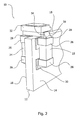
- a printed circuit board assembly 10 in accordance with the present invention comprises a printed circuit board 12 (PCB) with two major mounting surfaces 14 and 16, each surface having a plurality of conductive traces (not shown) and mounting pads 20 or lands.
- the PCB 12 also has an edge surface 18, substantially orthogonal to both major surfaces 14 and 16.
- the printed circuit board assembly 10 further comprises a first electronic component 22 mounted on a first major surface 14 and a second electronic component 24 mounted on a second major surface 16.
- Each of the first and second electronic components 22 and 24 has two contact terminals 26 mounted onto PCB mounting pads 20, for example by way of reflow soldering.
- the electronic components 22 and 24 may be mounted by welding, or using a conducting adhesive or by any other method known in the art.
- the first and second electronic components 22, 24 are SMT type resistors.
- SMT resistors are available in different forms and sizes and are cheap. These components may form a part of circuitry or may be used only for mounting edge components over them, in the latter case zero ohm resistors may be used, or the component terminals 26 may be electrically connected to one another or shortened by conductive traces on the PCB 12.
- End parts 28 of the contact terminals 26 which are aligned with the edge surface 18 serve as a mounting pads for a third electronic component 32 ( FIG. 2 ).
- the third electronic component 32 in this example, a light emitting diode (LED) in surface mount package, NSSW100 of Nichia, is surface mounted onto the end parts 28 of the contact terminals 26 by any surface mount method known in the art.
- LED light emitting diode
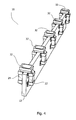
- the assembly 10 may contain a plurality or an array of such components 32. It is also apparent to those skilled in the art that the edge component 32 may have more than two terminals 34.
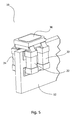
- FIG. 5 is shown an example of a printed circuit board assembly 10 with an edge mounted LED package 36, NSSM026AB of Nichia, having four terminals. There are SMT LED packages having six terminals, for example NSSM0116D of Nichia, that also may be used in embodiments of the present invention.
- the process of assembling the printed board assembly may include the following steps. Step one: providing a PCB having a first major surface, a second major surface, and an edge surface. Step two: mounting electronic components on first and second major surfaces by any method known in the art, preferably by SMT. Step three: applying solder on the end parts 28 of the contact terminals 26 of the electronic components 22 and 24 mounted on both major surfaces of the PCB 12, for example by solder print process. This may involve the use of a stencil fabricated with apertures at certain specified positions. The stencil is positioned above the edge PCB surface such that apertures in the stencil are positioned above each end part 28 of the contact terminals 26 of the electronic components 22 and 24.
- Solder is applied on the stencil and forced through the apertures in the stencil by a squeegee so that a desired amount of solder is deposited on the end parts 28 of the contact terminals 26.
- the PCB is then separated from the stencil, and the edge components 32 are placed atop the end parts 28.
- solder may be applied to the contacts terminals by direct solder paste dispensing using solder past dispenser equipment instead of solder print process.
- the PCB assembly is then put through a solder reflow process where controlled heating is used to melt the solder.
- the PCB assembly is then allowed to cool, and as the solder solidifies, it bonds each terminal 34 of the edge component 32 to the corresponding end part 28 of the contact terminals 26 of the electronic components 22 and 24.
Landscapes
- Engineering & Computer Science (AREA)
- Manufacturing & Machinery (AREA)
- Microelectronics & Electronic Packaging (AREA)
- Supply And Installment Of Electrical Components (AREA)
- Electric Connection Of Electric Components To Printed Circuits (AREA)
- Led Device Packages (AREA)
Priority Applications (1)
| Application Number | Priority Date | Filing Date | Title |
|---|---|---|---|
| EP08010446A EP2134146A1 (fr) | 2008-06-09 | 2008-06-09 | Ensemble de carte à circuit imprimé et procédé d'assemblage de celui-ci |
Applications Claiming Priority (1)
| Application Number | Priority Date | Filing Date | Title |
|---|---|---|---|
| EP08010446A EP2134146A1 (fr) | 2008-06-09 | 2008-06-09 | Ensemble de carte à circuit imprimé et procédé d'assemblage de celui-ci |
Publications (1)
| Publication Number | Publication Date |
|---|---|
| EP2134146A1 true EP2134146A1 (fr) | 2009-12-16 |
Family
ID=39855100
Family Applications (1)
| Application Number | Title | Priority Date | Filing Date |
|---|---|---|---|
| EP08010446A Withdrawn EP2134146A1 (fr) | 2008-06-09 | 2008-06-09 | Ensemble de carte à circuit imprimé et procédé d'assemblage de celui-ci |
Country Status (1)
| Country | Link |
|---|---|
| EP (1) | EP2134146A1 (fr) |
Cited By (3)
| Publication number | Priority date | Publication date | Assignee | Title |
|---|---|---|---|---|
| US10041657B2 (en) | 2016-06-13 | 2018-08-07 | Rebo Lighting & Electronics, Llc | Clip unit and edge mounted light emitting diode (LED) assembly comprising a clip unit |
| CN113966075A (zh) * | 2020-07-20 | 2022-01-21 | Atl技术有限公司 | 具有端部安装到印刷电路板的电部件的装置 |
| US12250770B2 (en) | 2020-04-15 | 2025-03-11 | Nokia Solutions And Networks Oy | Board edge electrical contact structures |
Citations (9)
| Publication number | Priority date | Publication date | Assignee | Title |
|---|---|---|---|---|
| DE4033199A1 (de) * | 1990-10-19 | 1992-04-23 | Kawe Electronic Gmbh & Co Kg | Verfahren zur herstellung von schaltungskarten mit miniatur-durchsteckbauelementen |
| JPH04148583A (ja) * | 1990-10-12 | 1992-05-21 | Fujitsu Ltd | 表面実装部品 |
| JPH06260374A (ja) * | 1993-03-02 | 1994-09-16 | Nippon Chemicon Corp | 固体電解コンデンサ |
| DE29820249U1 (de) * | 1998-11-12 | 1999-04-08 | Maisberger, Markus, 82194 Gröbenzell | LED-Stecksockel-Beleuchtungseinsatz |
| EP1383363A2 (fr) | 2002-07-19 | 2004-01-21 | Gamesman Limited | Carte de circuit imprimé avec lampes directement montées |
| EP1465468A1 (fr) * | 2003-03-31 | 2004-10-06 | SANYO ELECTRIC Co., Ltd. | Masque métallique et procédé pour imprimer de la pâte à souder sans plomb en utilisant celui-ci |
| WO2005072033A1 (fr) * | 2004-01-27 | 2005-08-04 | Matsushita Electric Industrial Co., Ltd. | Carte de circuit et procede de montage de puce |
| US20060065432A1 (en) * | 2004-09-29 | 2006-03-30 | Hitachi Cable, Ltd. | Mounting structure for electronic components |
| US20070030679A1 (en) | 2005-08-07 | 2007-02-08 | Chih-Jen Lee | Light emitting diode display device |
-
2008
- 2008-06-09 EP EP08010446A patent/EP2134146A1/fr not_active Withdrawn
Patent Citations (10)
| Publication number | Priority date | Publication date | Assignee | Title |
|---|---|---|---|---|
| JPH04148583A (ja) * | 1990-10-12 | 1992-05-21 | Fujitsu Ltd | 表面実装部品 |
| DE4033199A1 (de) * | 1990-10-19 | 1992-04-23 | Kawe Electronic Gmbh & Co Kg | Verfahren zur herstellung von schaltungskarten mit miniatur-durchsteckbauelementen |
| JPH06260374A (ja) * | 1993-03-02 | 1994-09-16 | Nippon Chemicon Corp | 固体電解コンデンサ |
| DE29820249U1 (de) * | 1998-11-12 | 1999-04-08 | Maisberger, Markus, 82194 Gröbenzell | LED-Stecksockel-Beleuchtungseinsatz |
| EP1383363A2 (fr) | 2002-07-19 | 2004-01-21 | Gamesman Limited | Carte de circuit imprimé avec lampes directement montées |
| EP1465468A1 (fr) * | 2003-03-31 | 2004-10-06 | SANYO ELECTRIC Co., Ltd. | Masque métallique et procédé pour imprimer de la pâte à souder sans plomb en utilisant celui-ci |
| WO2005072033A1 (fr) * | 2004-01-27 | 2005-08-04 | Matsushita Electric Industrial Co., Ltd. | Carte de circuit et procede de montage de puce |
| US20070145575A1 (en) * | 2004-01-27 | 2007-06-28 | Masato Mori | Circuit board and method for mounting chip component |
| US20060065432A1 (en) * | 2004-09-29 | 2006-03-30 | Hitachi Cable, Ltd. | Mounting structure for electronic components |
| US20070030679A1 (en) | 2005-08-07 | 2007-02-08 | Chih-Jen Lee | Light emitting diode display device |
Cited By (3)
| Publication number | Priority date | Publication date | Assignee | Title |
|---|---|---|---|---|
| US10041657B2 (en) | 2016-06-13 | 2018-08-07 | Rebo Lighting & Electronics, Llc | Clip unit and edge mounted light emitting diode (LED) assembly comprising a clip unit |
| US12250770B2 (en) | 2020-04-15 | 2025-03-11 | Nokia Solutions And Networks Oy | Board edge electrical contact structures |
| CN113966075A (zh) * | 2020-07-20 | 2022-01-21 | Atl技术有限公司 | 具有端部安装到印刷电路板的电部件的装置 |
Similar Documents
| Publication | Publication Date | Title |
|---|---|---|
| US7723855B2 (en) | Pad and circuit board, electronic device using same | |
| AU2008201050A1 (en) | Electronic-component-mounting board | |
| US20110094788A1 (en) | Printed circuit board with insulating areas | |
| KR100353231B1 (ko) | 프린트배선판 제조방법 및 프린트배선판과 그들에사용되는 양면패턴도통용 부품 | |
| CN216146514U (zh) | 电路板及电子装置 | |
| US20210092845A1 (en) | Connecting circuit boards using functional components | |
| US20040238205A1 (en) | Printed circuit board with controlled solder shunts | |
| US20080032523A1 (en) | Circuit module and manufacturing process thereof | |
| US8094460B2 (en) | Orientation-tolerant land pattern and method of manufacturing the same | |
| CN105848415A (zh) | 侧边具有表面黏着型接脚的电路模块以及电路板与系统 | |
| US6111758A (en) | Electronic component having alternate functionalities | |
| JP2016082074A (ja) | 電装装置およびその製造方法 | |
| JP3424685B2 (ja) | 電子回路装置とその製造方法 | |
| US5880935A (en) | Device for using in an electronic controller | |
| JP2004303944A (ja) | モジュール基板及びその製造方法 | |
| US20130322034A1 (en) | Method of Manufacturing a Surface Mounted Device and Corresponding Surface Mounted Device | |
| US20040119155A1 (en) | Metal wiring board and method for manufacturing the same | |
| JPH01312892A (ja) | 回路基板の製造方法 | |
| CN115279059B (zh) | 一种小间距波峰物料及其焊接方法 | |
| KR100287738B1 (ko) | 인쇄회로기판용 표면실장 방법 | |
| US20070184688A1 (en) | Interconnection device for a double-sided printed circuit board | |
| US20060213058A1 (en) | Circuit board for surface-mount device to be mounted thereon | |
| JP5087049B2 (ja) | プリント基板用端子 | |
| CN108668463A (zh) | 一种轴向封装元件的焊接方法 | |
| JP7462502B2 (ja) | 部品実装基板及びその製造方法 |
Legal Events
| Date | Code | Title | Description |
|---|---|---|---|
| PUAI | Public reference made under article 153(3) epc to a published international application that has entered the european phase |
Free format text: ORIGINAL CODE: 0009012 |
|
| AK | Designated contracting states |
Kind code of ref document: A1 Designated state(s): AT BE BG CH CY CZ DE DK EE ES FI FR GB GR HR HU IE IS IT LI LT LU LV MC MT NL NO PL PT RO SE SI SK TR |
|
| AX | Request for extension of the european patent |
Extension state: AL BA MK RS |
|
| AKY | No designation fees paid | ||
| REG | Reference to a national code |
Ref country code: DE Ref legal event code: 8566 |
|
| STAA | Information on the status of an ep patent application or granted ep patent |
Free format text: STATUS: THE APPLICATION IS DEEMED TO BE WITHDRAWN |
|
| 18D | Application deemed to be withdrawn |
Effective date: 20100617 |