EP2136406A1 - Transistor à couche mince, son procédé de fabrication et dispositif à écran plat doté de celui-ci - Google Patents
Transistor à couche mince, son procédé de fabrication et dispositif à écran plat doté de celui-ci Download PDFInfo
- Publication number
- EP2136406A1 EP2136406A1 EP09251375A EP09251375A EP2136406A1 EP 2136406 A1 EP2136406 A1 EP 2136406A1 EP 09251375 A EP09251375 A EP 09251375A EP 09251375 A EP09251375 A EP 09251375A EP 2136406 A1 EP2136406 A1 EP 2136406A1
- Authority
- EP
- European Patent Office
- Prior art keywords
- electrode
- layer
- oxide semiconductor
- thin film
- film transistor
- Prior art date
- Legal status (The legal status is an assumption and is not a legal conclusion. Google has not performed a legal analysis and makes no representation as to the accuracy of the status listed.)
- Granted
Links
Images



Classifications
-
- H—ELECTRICITY
- H10—SEMICONDUCTOR DEVICES; ELECTRIC SOLID-STATE DEVICES NOT OTHERWISE PROVIDED FOR
- H10D—INORGANIC ELECTRIC SEMICONDUCTOR DEVICES
- H10D30/00—Field-effect transistors [FET]
- H10D30/60—Insulated-gate field-effect transistors [IGFET]
- H10D30/67—Thin-film transistors [TFT]
- H10D30/6729—Thin-film transistors [TFT] characterised by the electrodes
- H10D30/6737—Thin-film transistors [TFT] characterised by the electrodes characterised by the electrode materials
-
- G—PHYSICS
- G02—OPTICS
- G02F—OPTICAL DEVICES OR ARRANGEMENTS FOR THE CONTROL OF LIGHT BY MODIFICATION OF THE OPTICAL PROPERTIES OF THE MEDIA OF THE ELEMENTS INVOLVED THEREIN; NON-LINEAR OPTICS; FREQUENCY-CHANGING OF LIGHT; OPTICAL LOGIC ELEMENTS; OPTICAL ANALOGUE/DIGITAL CONVERTERS
- G02F1/00—Devices or arrangements for the control of the intensity, colour, phase, polarisation or direction of light arriving from an independent light source, e.g. switching, gating or modulating; Non-linear optics
- G02F1/01—Devices or arrangements for the control of the intensity, colour, phase, polarisation or direction of light arriving from an independent light source, e.g. switching, gating or modulating; Non-linear optics for the control of the intensity, phase, polarisation or colour
- G02F1/13—Devices or arrangements for the control of the intensity, colour, phase, polarisation or direction of light arriving from an independent light source, e.g. switching, gating or modulating; Non-linear optics for the control of the intensity, phase, polarisation or colour based on liquid crystals, e.g. single liquid crystal display cells
- G02F1/133—Constructional arrangements; Operation of liquid crystal cells; Circuit arrangements
- G02F1/136—Liquid crystal cells structurally associated with a semi-conducting layer or substrate, e.g. cells forming part of an integrated circuit
- G02F1/1362—Active matrix addressed cells
- G02F1/1368—Active matrix addressed cells in which the switching element is a three-electrode device
-
- H—ELECTRICITY
- H10—SEMICONDUCTOR DEVICES; ELECTRIC SOLID-STATE DEVICES NOT OTHERWISE PROVIDED FOR
- H10D—INORGANIC ELECTRIC SEMICONDUCTOR DEVICES
- H10D30/00—Field-effect transistors [FET]
- H10D30/60—Insulated-gate field-effect transistors [IGFET]
- H10D30/67—Thin-film transistors [TFT]
- H10D30/674—Thin-film transistors [TFT] characterised by the active materials
- H10D30/6755—Oxide semiconductors, e.g. zinc oxide, copper aluminium oxide or cadmium stannate
-
- H—ELECTRICITY
- H10—SEMICONDUCTOR DEVICES; ELECTRIC SOLID-STATE DEVICES NOT OTHERWISE PROVIDED FOR
- H10D—INORGANIC ELECTRIC SEMICONDUCTOR DEVICES
- H10D64/00—Electrodes of devices having potential barriers
- H10D64/60—Electrodes characterised by their materials
- H10D64/62—Electrodes ohmically coupled to a semiconductor
Definitions
- the present invention relates to a thin film transistor. Particularly, but not exclusively, the invention relates to a thin film transistor that uses an oxide semiconductor as an active layer, a method of manufacturing the same, and a flat panel display device having the same.
- an active layer having a channel region, a source region, and a drain region is formed of a semiconductor, such as amorphous silicon or poly-silicon.
- a semiconductor such as amorphous silicon or poly-silicon.
- the active layer has low mobility so that it is difficult to operate a driving circuit at a high speed.
- the active layer is formed of poly-silicon, the active layer has a high mobility but a non-uniform threshold voltage so that a separate compensation circuit is necessary.
- the thin film transistor using zinc oxide (ZnO) or an oxide semiconductor mainly constituted by the zinc oxide (ZnO) as the active layer is disclosed in the Japanese Patent Publication No. 2004-273614 .
- a conventional thin film transistor using the oxide semiconductor as the active layer has poor ohmic contact with a metal electrode due to a wide band gap of the oxide semiconductor.
- aspects of the present invention provide a thin film transistor, a method of manufacturing the same, and a flat panel display device having the same capable of improving ohmic contact characteristics of an oxide semiconductor layer and a metal electrode.
- a thin film transistor including: a substrate; an oxide semiconductor layer formed on the substrate and having a channel region, a source region, and a drain region; a gate insulating layer formed on the substrate to cover the oxide semiconductor layer; a gate electrode formed on the gate insulating layer and insulated from the oxide semiconductor layer by the gate insulating layer; an ohmic contact layer formed on the source region and the drain region of the oxide semiconductor layer; and a source electrode and a drain electrode respectively electrically coupled to the source region and the drain region through the ohmic contact layer, wherein the ohmic contact layer is formed of a metal having a lower work function than work functions of the source electrode and the drain electrode.
- aspects of present invention provide a method of manufacturing a thin film transistor including: forming a gate electrode on a substrate; forming a gate insulating layer on the gate electrode; forming an oxide semiconductor layer having a channel region, a source region, and a drain region on the gate insulating layer; forming an ohmic contact layer on the source region and the drain region of the oxide semiconductor layer; and forming a source electrode and a drain electrode respectively electrically coupled to the source region and the drain region through the ohmic contact layer, wherein the ohmic contact layer is formed of a metal having a lower work function than the source electrode and the drain electrode.
- a flat panel display device having a thin film transistor including: a first substrate having disposed thereon first and second conductive lines, the first conductive lines disposed to cross the second conductive lines, a plurality of pixels, each of the plurality of pixels having a first electrode and being defined by the first conductive lines and the second conductive lines, a plurality of thin film transistors electrically coupled to the first electrodes to control signals supplied to each of the pixels, respectively; a second substrate having a second electrode formed thereon; and a liquid crystal layer disposed in a sealed space between the first electrode and the second electrode, wherein each of the thin film transistors includes: a gate electrode electrically connected to one of the first and second conductive lines; an ohmic contact layer formed on the source region and the drain region of the oxide semiconductor layer; and a source electrode and a drain electrode respectively electrically coupled to the source region and the drain region through the ohmic contact layer, one of the source electrode and the drain electrode being electrically connected
- a flat panel display device having a thin film transistor including: a first substrate having disposed thereon an organic light emitting element including a first electrode, an organic thin film layer, and a second electrode, scan and data lines, and a thin film transistor to control operation of the organic light emitting element; and a second substrate disposed to face the first substrate, wherein the thin film transistor includes: a gate electrode electrically connected to one of the scan lines; an ohmic contact layer formed on a source region and a drain region of an oxide semiconductor layer; and a source electrode and a drain electrode respectively electrically coupled to the source region and the drain region through the ohmic contact layer, one of the source electrode and the drain electrode being electrically connected to one of the data lines, and the other of the source electrode and the drain electrode being electrically connected to the first electrode, wherein the ohmic contact layer is formed of a metal having a lower work function than work functions of the source electrode and the drain electrode.
- a thin film transistor including: a substrate; a gate electrode formed on the substrate; a gate insulating layer formed on the substrate to cover the gate electrode; an oxide semiconductor layer formed on the gate insulating layer, the oxide semiconductor layer being insulated from the gate electrode by the gate insulating layer, and the oxide semiconductor layer having a channel region, a source region, and a drain region; an ohmic contact layer formed on the source region and the drain region of the oxide semiconductor layer; and a source electrode and a drain electrode respectively electrically coupled to the source region and the drain region through the ohmic contact layer, wherein the ohmic contact layer is formed of a metal having a lower work function than work functions of the source electrode and the drain electrode.
- aspects of present invention provide a method of manufacturing a thin film transistor, the method including: forming an oxide semiconductor layer having a channel region, a source region, and a drain region on a substrate; forming a gate insulating layer on the oxide semiconductor layer; forming a gate electrode on the gate insulating layer; forming via holes in the gate insulating layer to expose portions of the source region and the drain region; forming an ohmic contact layer on the exposed portions of the source region and the drain region; and forming a source electrode and a drain electrode respectively electrically coupled to the source region and the drain region through the ohmic contact layer.
- aspects of present invention provide a method of manufacturing a thin film transistor, the method including: forming an oxide semiconductor layer having a channel region, a source region, and a drain region on a substrate; forming an ohmic contact layer on the source region and the drain region; forming a gate insulating layer on the oxide semiconductor layer; forming a gate electrode on the gate insulating layer; forming via holes in the gate insulating layer to expose portions of the ohmic contact layer on the source region and the drain region; and forming a source electrode and a drain electrode respectively electrically coupled to the source region and the drain region through the ohmic contact layer, wherein the ohmic contact layer is formed of a metal having a lower work function than work functions of the source electrode and the drain electrode.
- the ohmic contact layer is formed between the oxide semiconductor layer and the metal electrode and of the metal or an alloy thereof having a low function. Therefore, height of a Schottky barrier is reduced by the ohmic contact layer so that contact resistance between the oxide semiconductor layer and the source and drain electrodes is lowered. Thereby, a current-voltage characteristic is improved so that an electrical characteristic of the device may be improved.
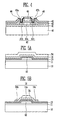
- FIG. 1 is a cross-sectional view of a thin film transistor according to a first embodiment of the present invention, wherein an example of a bottom gate structure is shown. Although explained with respect to a bottom gate thin film transistor, aspects of the present invention may also be applied to a top gate thin film transistor.
- a buffer layer 11 is formed on a substrate 10, and a gate electrode 12 is formed on the buffer layer 11.
- a gate insulating layer 13 is formed on an upper surface of the substrate 10 on which the gate electrode 12 is formed.
- An oxide semiconductor layer 14 is formed as an active layer having a channel region 14a, a source region 14b, and a drain region 14c and formed on the gate insulating layer 13 corresponding to the gate electrode 12.
- An ohmic contact layer 15 is formed on the source region 14b and the drain region 14c of the oxide semiconductor layer 14. Also, source and drain electrodes 16a and 16b are formed to contact the source region 14b and the drain region 14c through the ohmic contact layer 15.
- the oxide semiconductor layer 14 includes zinc oxide (ZnO), and may be doped with at least one ion of gallium (Ga), indium (In), tin (Sn), zirconium (Zr), hafnium (Hf), cadmium (Cd), silver (Ag), copper (Cu), germanium (Ge), gadolinium (Gd), and vanadium (V).
- the oxide semiconductor layer 14 may be formed of ZnO, ZnGaO, ZnlnO, ZnSnO, GalnZnO, CdO, InO, GaO, SnO, AgO, CuO, GeO, GdO, HfO, etc., for example.
- the ohmic contact layer 15 reduces contact resistance between the source region 14b and the drain region 14c of the oxide semiconductor layer 14 and the source and drain electrodes 16a and 16b, which are made of a metal. Accordingly, the ohmic contact layer 15 is formed of a metal having a lower work function than a work function of a metal from which the source and drain electrodes 16a and 16b are formed.
- the source and drain electrodes 16a and 16b are formed of a metal, such as molybdenum (Mo), tungsten (W), aluminum (Al), titanium (Ti), etc.
- the work functions of these metals is approximately 4 eV or more. Therefore, the ohmic contact layer 15 is formed of a metal with work function of 2 to 4 eV.
- a metal includes an alkali metal such as calcium (Ca) (2.9 eV), magnesium (Mg) (3.7 eV), potassium (K) (2.3 eV), lithium (Li) (2.9 eV), etc.
- an alkali metal has a chemically high reactivity, the alkali metal may be easily changed by a chemical reaction.
- the ohmic contact layer 15 may be formed of an alloy, such as magnesium-silver (Mg-Ag), lithium-aluminum (Li-Al), aluminum-silver (Al-Ag), lithium-fluorine (LiF), etc., in order to prevent such chemical change.
- an alloy such as magnesium-silver (Mg-Ag), lithium-aluminum (Li-Al), aluminum-silver (Al-Ag), lithium-fluorine (LiF), etc.
- FIG. 2 is a cross-sectional view of a thin film transistor according to a second embodiment of the present invention. Herein, only the differences between the structures shown in FIG. 1 and FIG. 2 will be described.
- the thin film transistor in FIG. 1 has a structure that the ohmic contact layer 15 is formed only on the source region 14b and the drain region 14c of the oxide semiconductor layer 14.
- the thin film transistor in FIG. 2 has a structure that an ohmic contact layer 25 is formed on lower surfaces of the source and drain electrodes 16a and 16b.
- the ohmic contact layer 25 is formed to overlap the source and drain electrodes 16a and 16b. Therefore, it is possible to pattern the ohmic contact layer 25 and the source and drain electrodes 16a and 16b with one mask, thereby decreasing mask numbers and process steps as compared to FIG. 1 .
- FIG. 3 is a cross-sectional view of a thin film transistor according to a third embodiment of the present invention.
- the thin film transistor in FIG. 1 has a structure that the channel region 14a of the oxide semiconductor layer 14 is exposed
- the thin film transistor in FIG. 3 has a structure that a passivation layer 34 is formed on the channel region 14a of the oxide semiconductor layer 14.
- the passivation layer 34 is formed of an inorganic material or an insulating organic material, such as a polyimide-based resin, etc.
- the oxide semiconductor layer 14 is easily damaged by plasma or easily etched by acid chemicals, etc. Therefore, in the structure that the oxide semiconductor layer 14 is exposed, when forming a thin film thereon or etching a formed thin film, damage may occur so that a change in an electrical characteristic, such as increase of carriers, occurs. Because of such a change in the electrical characteristic of the oxide semiconductor layer 14, an electrical characteristic of the thin film transistor may be deteriorated and a dispersive degree of the electrical characteristics in the substrate may be deteriorated.
- the channel region 14a of the oxide semiconductor layer 14 is protected by the passivation layer 34 and at the same time, the passivation layer 34 may be used as an etch stop layer. Therefore, the damage of the oxide semiconductor layer 14 by the plasma or the acid chemicals is effectively prevented and at the same time, the process is simplified.
- FIG. 4 a cross-sectional view of a thin film transistor according to a fourth embodiment of the present invention, wherein an example of a top gate structure is shown.
- a buffer layer 41 is formed on a substrate 40, and an oxide semiconductor layer 42 is formed as an active layer having a channel region 42a, a source region 42b, and a drain region 42c on the buffer layer 41.
- a gate insulating layer 43 is formed on an upper surface of the oxide semiconductor layer 42, and a gate electrode 44 is formed on the gate insulating layer 43 on an upper surface of the oxide semiconductor layer 42, i.e., the gate electrode is formed on the gate insulating layer 43 in an area corresponding to the oxide semiconductor layer 42.
- An insulating layer 45 is formed on an upper surface to cover the gate electrode 44, and contact holes are formed in the insulating layer 45 and the gate insulating layer 43 so that portions of the source region 42b and the drain region 42c of the oxide semiconductor layer 42are exposed.
- An ohmic contact layer 46 is formed to cover surfaces of the contact holes formed in the insulating layer 45 and the gate insulating layer 43. The ohmic contact layer 46 further covers the exposed portions of the source region 42b and the drain region 42c of the oxide semiconductor layer 42 exposed through the contact holes.
- Source and drain electrodes 47a and 47b are formed to be coupled to the source region 42b and the drain region 42c through the ohmic contact layer 46.
- the ohmic contact layer 46 may also be formed only on the exposed portions of the oxide semiconductor layer 42. Further, the ohmic contact layer 46 may be formed on the entire source and drain regions 42b and 42c of the oxide semiconductor region 42, between the source and drain regions 42b and 42c and the gate insulating layer 43.
- the oxide semiconductor layer 42 includes zinc oxide (ZnO), and may be doped with at least one ion of gallium (Ga), indium (In), tin (Sn), zirconium (Zr), hafnium (Hf), cadmium (Cd), silver (Ag), copper (Cu), germanium (Ge), gadolinium (Gd), and vanadium (V).
- the oxide semiconductor layer 42 may be formed of ZnO, ZnGaO, ZnInO, ZnSnO, GaInZnO, CdO, InO, GaO, SnO, AgO, CuO, GeO, GdO, HfO, etc., for example.
- the ohmic contact layer 46 reduces contact resistance between the source region 42b and the drain region 42c of oxide semiconductor layer 42 and the source and drain electrodes 47a and 47b, which are made of a metal. Accordingly, the ohmic contact layer 46 is formed of a metal having a work function lower than a work function of a metal from which the source and drain electrodes 47a and 47b are formed.
- the source and drain electrodes 47a and 47b are formed of a metal, such as molybdenum (Mo), tungsten (W), aluminum (Al), titanium (Ti), etc.
- the work functions of these metals are approximately 4 eV or more. Therefore, the ohmic contact layer 15 is formed of a metal with the work function of about 2 to 4 eV.
- a metal includes an alkali metal, such as calcium (Ca) (2.9 eV), magnesium (Mg) (3.7 eV), potassium (K) (2.3 eV), lithium (Li) (2.9 eV), etc.
- an alkali metal has a chemically high reactivity, it may be easily changed by a chemical reaction.
- the ohmic contact layer 15 may be formed of an alloy, such as magnesium-silver (Mg-Ag), lithium-aluminum (Li-Al), aluminum-silver (Al-Ag), lithium-fluorine (LiF), etc., in order to prevent such chemical change.
- an alloy such as magnesium-silver (Mg-Ag), lithium-aluminum (Li-Al), aluminum-silver (Al-Ag), lithium-fluorine (LiF), etc.
- FIGs. 5A to 5E are cross-sectional views illustrating a method of manufacturing a thin film transistor according to aspects of the present invention.
- the structure in FIG. 3 will be explained as an example.
- the gate electrode 12 is formed on the buffer layer 11.
- the gate insulating layer 13, the oxide semiconductor layer 14, and the passivation layer 34 are sequentially formed on the upper surface of the substrate having the gate electrode 12 formed thereon.
- a semiconductor substrate such as silicon (Si)
- an insulating substrate such as glass or plastic, or a metal substrate
- the gate electrode 12 is formed of a metal such, as Al, Cr, MoW, etc.
- the gate insulating layer 13 is formed of an insulating material, such as SiO 2 , SiN x , GaO 3 , etc.
- the oxide semiconductor layer 14 includes zinc oxide (ZnO), wherein the ZnO may be doped with at least one ion of gallium (Ga), indium (In), tin (Sn), zirconium (Zr), hafnium (Hf), cadmium (Cd), silver (Ag), copper (Cu), germanium (Ge), gadolinium (Gd), and vanadium (V).
- the oxide semiconductor layer 14 is formed of ZnO, ZnGaO, ZnInO, ZnSnO, GaInZnO, CdO, InO, GaO, SnO, AgO, CuO, GeO, GdO, HfO, etc., for example.
- the passivation layer 34 is formed of an inorganic material or an insulating organic material, such as a polyimide-based resin, etc.
- the oxide semiconductor layer 14 is patterned so that a channel region 14a, a source region 14b, and a drain region 14c are defined, and the passivation layer 34 is patterned so that it remains only on the channel region 14a of the oxide semiconductor 14.
- the ohmic contact layer 15 is patterned so that it remains only on the source region 14b and the drain region 14c of the oxide semiconductor layer 14 and the passivation layer 34, i.e., the ohmic contact layer 15 is patterned to correspond to areas on which source and drain electrodes 16a and 16b are to be formed.
- the ohmic contact layer 15 may be patterned as described above with respect to FIGs. 1-4 .
- the source and drain electrodes 16a and 16b are formed to be coupled to the source region 14b and the drain region 14c through the ohmic contact layer 15.
- the source and drain electrodes 16a and 16b are formed of a metal, such as molybdenum (Mo), tungsten (W), aluminum (Al), titanium (Ti), or are formed of an alloy thereof.
- Mo molybdenum
- W tungsten
- Al aluminum
- Ti titanium
- the source and drain electrodes 16a and 16b may be formed in a stacked structure of the metal and/or alloy thereof.
- the source and drain electrodes 16a and 16b may be formed of a transparent conductive material, such as indium tin oxide (ITO), indium zinc oxide (IZO), indium tin zinc oxide (ITZO), etc.
- ITO indium tin oxide
- IZO indium zinc oxide
- ITZO indium tin zinc oxide
- FIG. 5E it is possible to irradiate plasma on the exposed source and drain regions 14b and 14c on both sides of the passivation layer 34 in the operation of patterning the oxide semiconductor layer 14 and the passivation layer 34 as in FIG. 5B .
- oxygen vacancy occurs due to lattice damage by the plasma.
- electric conductivities of surfaces of the source region 14b and the drain region 14c increase so that contact resistance between the source region 14b and the drain region 14c of the oxide semiconductor layer 14 and the source and drain electrodes 16a and 16b may be effectively reduced.
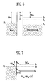
- FIG. 6 is a band diagram before junction of a metal and an oxide semiconductor (for example, ZnO), wherein the work function of the metal is larger than that of an n-type oxide semiconductor ( ⁇ m > ⁇ s).
- the conduction band E C and the valence band E V are indicated for the semiconductor, and the Fermi energies E F of both the metal and the semiconductor are indicated.
- a general metal corresponds to such a band diagram.
- FIG. 7 is a band diagram after the junction of the metal and the oxide semiconductor (for example, ZnO), wherein some electrons of the oxide semiconductor are diffused toward the metal so that a depletion region is formed in the oxide semiconductor in the vicinity of the interface between metal and the oxide semiconductor.
- the contact resistance Rc may be indicated as in Equation. 1 below.
- T indicates a temperature
- A indicates a Richardson constant
- k indicates a Boltzmann constant
- q ⁇ Bn indicates the Schottky barrier.
- a height of the Schottky barrier is determined by the electron affinity of the metal and the oxide semiconductor. As the work function of the metal becomes smaller, the height of the Schottky barrier is reduced so that the contact resistance is reduced.
- FIG. 8 is a band diagram after the junction of the metal and the oxide semiconductor (for example, ZnO) in the case where a number of surface states exist on a surface of the oxide semiconductor, wherein the electron on the surface of the oxide semiconductor is trapped in an interface state so that the depletion region is formed. This is referred to as Fermi level pinning.
- the oxide semiconductor for example, ZnO
- FIG. 9 is a band diagram after the junction of the metal and a Fermi level pinned oxide semiconductor. At this time, the height of the Schottky barrier is independent of the work function of the metal. This is referred to as the Bardeen limit.
- the ohmic contact layer is formed of the metal with a low work function between the oxide semiconductor layer and the metal electrode.
- the height of the Schottky barrier is reduced by the ohmic contact layer so that the contact resistance between the oxide semiconductor layer and the metal electrode is reduced. Thereby, current-voltage characteristics of the thin film transistor may be improved.
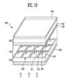
- FIG. 10 is a perspective view of a flat panel display device having a thin film transistor according to aspects of the present invention.
- a display panel 100 to display an image will be described.
- the display panel 100 comprises two substrates 110 and 120 disposed to face each other and a liquid crystal layer 130 disposed between the two substrates 110 and 120.
- a pixel region 113 is defined by a plurality of scan lines 111 and a plurality of data lines 112 arranged in a matrix form on the substrate 110.
- a thin film transistor 114 to control signals supplied to each pixel and a pixel electrode 115 coupled to the thin film transistor 114 are formed on the substrate 110 in each of the pixel regions 113.
- the thin film transistor 114 has any one of the structures in FIGs. 1 to 4 , and may be manufactured according to the method described with reference to FIGs. 5A to 5E .
- a color filter 121 and a common electrode 122 are formed on the substrate 120.
- Polarizing plates 116 and 123 are formed on rear surfaces of the substrates 110 and 120, respectively, and a backlight (not shown) is disposed as a light source under the polarizing plate 116.
- a driver (LCD drive IC, not shown) to drive the display panel 100 is mounted in the circumferential area of the pixel region 113 of the display panel 100.
- the driver converts an electrical signal provided from the outside into a scan signal and a data signal to supply them to the scan lines 111 and the data lines 112.
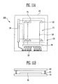
- FIGs. 11A and 11B are a plan view and a cross-sectional view of a flat panel display device having a thin film transistor according to aspects of the present invention.
- a display panel 200 to display an image will be described.
- a substrate 210 includes a pixel region 220 and a non-pixel region 230 surrounding the pixel region 220.
- a plurality of organic light emitting elements 300 coupled in a matrix form between scan lines 224 and data lines 226 are formed on the substrate 210 in the pixel region 220.
- a scan line 224 and a data line 226 extends from the pixel region 220 to the non-pixel region 230 and are supplied with signals from a scan driver 234 and a data driver 236, respectively.
- a power supply line (not shown) supplies power to the organic light emitting element 300.
- the scan driver 234 and a data driver 236 process signals provided from the outside through a pad 228 to supply the processed signals to the scan line 224 and the data line 226, respectively.
- the scan driver 234, the data driver 236, the power supply line, and the pad are formed on the substrate 210 in the non-pixel region 230.
- the organic light emitting diode 300 comprises an anode electrode 317, a cathode electrode 320, and an organic thin film layer 319 formed between the anode electrode 317 and the cathode electrode 320.
- the organic thin film layer 319 is formed having a structure in which a hole transport layer, an organic light emitting layer, and an electron transport layer are stacked. Further, the organic thin film layer 319 may include a hole injection layer, a hole blocking layer, an electron blocking layer, and an electron injection layer, among others. Further, each of the layers of the organic light emitting diode 300 may include stacked layers. Also, the organic light emitting diode 300 can further include a thin film transistor to control the operation of the organic light emitting element 300 and a capacitor to maintain the signal.
- the thin film transistor may have any one of the structures in FIGs. 1 to 4 , and may be manufactured according to the manufacturing method described with reference to FIGs. 5A to 5E .
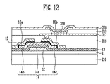
- the organic light emitting element 300 including the thin film transistor as described above will be described in detail with reference to FIGs. 11A and 12 .
- the buffer layer 11 is formed on the substrate 210 in the pixel region 220, and the gate electrode 12 is formed on the buffer layer 11.
- the pixel region 220 may be formed with the scan line 223 coupled to the gate electrode 12, and the non pixel region 230 may be formed with the scan line 224 extended from the pixel region 220 and the pad 228 that receives the signal from the outside.
- the oxide semiconductor layer 14 is formed on the gate insulating layer 13 on the gate electrode 12 and electrically insulated from the gate electrode 12 by the gate insulating layer 13.
- the ohmic contact layer 15 is formed on the source region 14b and the drain region 14c of the oxide semiconductor layer 14, and the source and drain electrodes 16a and the 16b are formed to be coupled to the source region 14b and the drain region 14c through the ohmic contact layer 15.
- the pixel region 220 may be formed with the data line 226 coupled to one of the source and drain electrodes 16a and 16b, and the non-pixel region 230 may be formed with the data line 226 extended from the pixel region 220 and the pad 228 that receives the signal from the outside.
- a planarization layer 316 to planarize the entire surface of the pixel region 220 is formed.
- a via-hole is formed in the planarization layer 316 so that a portion of the source electrode 16a or the drain electrode 16b is exposed, and the anode electrode 317 is formed and coupled to the source electrode 16a or the drain electrode 16b through the via-hole.
- a pixel definition film 318 is formed on the planarization layer 316 so that a partial region (light emitting region) of the anode region 317 is exposed, and the organic thin film layer 319 is formed on the exposed anode electrode 317.
- the cathode electrode 320 is formed on the pixel definition film 318 to cover the organic thin film layer 319.
- a sealing substrate 400 sealing the pixel region 220 is disposed on the upper surface of the substrate 210 on which the organic light emitting elements 300 are formed as described above.
- the sealing substrate 400 is bonded to the substrate 210 by a sealant 410 so that the display panel is completed.
Landscapes
- Physics & Mathematics (AREA)
- Nonlinear Science (AREA)
- Mathematical Physics (AREA)
- Engineering & Computer Science (AREA)
- Chemical & Material Sciences (AREA)
- Crystallography & Structural Chemistry (AREA)
- Microelectronics & Electronic Packaging (AREA)
- General Physics & Mathematics (AREA)
- Optics & Photonics (AREA)
- Electrodes Of Semiconductors (AREA)
- Thin Film Transistor (AREA)
- Liquid Crystal (AREA)
- Electroluminescent Light Sources (AREA)
Applications Claiming Priority (1)
| Application Number | Priority Date | Filing Date | Title |
|---|---|---|---|
| KR1020080057250A KR100958006B1 (ko) | 2008-06-18 | 2008-06-18 | 박막 트랜지스터, 그의 제조 방법 및 박막 트랜지스터를구비하는 평판 표시 장치 |
Publications (2)
| Publication Number | Publication Date |
|---|---|
| EP2136406A1 true EP2136406A1 (fr) | 2009-12-23 |
| EP2136406B1 EP2136406B1 (fr) | 2013-08-28 |
Family
ID=41066684
Family Applications (1)
| Application Number | Title | Priority Date | Filing Date |
|---|---|---|---|
| EP09251375.3A Not-in-force EP2136406B1 (fr) | 2008-06-18 | 2009-05-21 | Transistor à couche mince, son procédé de fabrication et dispositif à écran plat doté de celui-ci |
Country Status (5)
| Country | Link |
|---|---|
| US (1) | US20090315026A1 (fr) |
| EP (1) | EP2136406B1 (fr) |
| JP (1) | JP5274147B2 (fr) |
| KR (1) | KR100958006B1 (fr) |
| CN (1) | CN101609843A (fr) |
Cited By (9)
| Publication number | Priority date | Publication date | Assignee | Title |
|---|---|---|---|---|
| EP2158609A4 (fr) * | 2007-06-19 | 2010-07-14 | Samsung Electronics Co Ltd | Semi-conducteurs à oxyde et transistors à couche mince comprenant ces mêmes |
| EP2715786A4 (fr) * | 2011-06-08 | 2015-01-07 | Cbrite Inc | Transistor en couches minces (tft) d'oxyde métallique ayant des contacts améliorés source/drain |
| US9000443B2 (en) | 2010-01-20 | 2015-04-07 | Semiconductor Energy Laboratory Co., Ltd. | Light-emitting device, flexible light-emitting device, electronic device, lighting apparatus, and method of manufacturing light-emitting device and flexible-light emitting device |
| US9000442B2 (en) | 2010-01-20 | 2015-04-07 | Semiconductor Energy Laboratory Co., Ltd. | Light-emitting device, flexible light-emitting device, electronic device, and method for manufacturing light-emitting device and flexible-light emitting device |
| CN106298887A (zh) * | 2016-09-30 | 2017-01-04 | 中山大学 | 一种高阈值电压高迁移率凹槽栅mosfet的制备方法 |
| TWI567985B (zh) * | 2011-10-21 | 2017-01-21 | 半導體能源研究所股份有限公司 | 半導體裝置及其製造方法 |
| US9911858B2 (en) | 2010-12-28 | 2018-03-06 | Semiconductor Energy Laboratory Co., Ltd. | Semiconductor device and method for manufacturing the same |
| US20190312147A1 (en) * | 2012-04-02 | 2019-10-10 | Samsung Display Co., Ltd. | Thin film transistor, thin film transistor array panel including the same, and method of manufacturing the same |
| US20220077266A1 (en) * | 2016-04-01 | 2022-03-10 | Japan Display Inc. | Semiconductor device including a flexible substrate |
Families Citing this family (63)
| Publication number | Priority date | Publication date | Assignee | Title |
|---|---|---|---|---|
| TWI489628B (zh) * | 2009-04-02 | 2015-06-21 | 半導體能源研究所股份有限公司 | 半導體裝置和其製造方法 |
| CN102473731B (zh) | 2009-07-10 | 2015-06-17 | 株式会社半导体能源研究所 | 制造半导体器件的方法 |
| KR20220031135A (ko) | 2009-09-16 | 2022-03-11 | 가부시키가이샤 한도오따이 에네루기 켄큐쇼 | 표시 장치 |
| WO2011043162A1 (fr) * | 2009-10-09 | 2011-04-14 | Semiconductor Energy Laboratory Co., Ltd. | Dispositif à semi-conducteur et procédé pour fabriquer le dispositif à semi-conducteur |
| TWI467770B (zh) * | 2009-10-26 | 2015-01-01 | Prime View Int Co Ltd | 顯示器及其薄膜電晶體陣列基板與薄膜電晶體 |
| KR101523358B1 (ko) * | 2009-12-04 | 2015-05-27 | 가부시키가이샤 한도오따이 에네루기 켄큐쇼 | 표시 장치 |
| WO2011080998A1 (fr) * | 2009-12-28 | 2011-07-07 | Semiconductor Energy Laboratory Co., Ltd. | Dispositif semi-conducteur |
| WO2011089844A1 (fr) * | 2010-01-24 | 2011-07-28 | Semiconductor Energy Laboratory Co., Ltd. | Dispositif d'affichage et son procédé de fabrication |
| KR101791713B1 (ko) * | 2010-02-05 | 2017-10-30 | 가부시키가이샤 한도오따이 에네루기 켄큐쇼 | 전계 효과 트랜지스터 및 반도체 장치 |
| KR102026603B1 (ko) * | 2010-02-05 | 2019-10-01 | 가부시키가이샤 한도오따이 에네루기 켄큐쇼 | 반도체 장치 |
| KR101117737B1 (ko) | 2010-03-02 | 2012-02-24 | 삼성모바일디스플레이주식회사 | 유기 발광 표시 장치 |
| KR101280649B1 (ko) * | 2010-03-11 | 2013-07-01 | 샤프 가부시키가이샤 | 반도체 장치 및 그 제조 방법 |
| CN102918650B (zh) | 2010-04-07 | 2017-03-22 | 株式会社半导体能源研究所 | 晶体管 |
| KR101293130B1 (ko) * | 2010-05-28 | 2013-08-12 | 엘지디스플레이 주식회사 | 어레이 기판 및 이의 제조방법 |
| KR101108175B1 (ko) | 2010-06-09 | 2012-01-31 | 삼성모바일디스플레이주식회사 | 박막 트랜지스터, 이를 포함하는 디스플레이 장치용 어레이 기판 및 그 제조 방법 |
| WO2011162177A1 (fr) * | 2010-06-21 | 2011-12-29 | 株式会社アルバック | Dispositif à semi-conducteurs, et dispositif d'affichage à cristaux liquides ainsi que procédé de fabrication associés |
| KR101182232B1 (ko) | 2010-06-30 | 2012-09-12 | 삼성디스플레이 주식회사 | 유기전계발광 표시장치 |
| KR102765169B1 (ko) * | 2010-07-02 | 2025-02-06 | 가부시키가이샤 한도오따이 에네루기 켄큐쇼 | 반도체 장치 및 그 제작 방법 |
| CN106057144B (zh) * | 2010-07-02 | 2019-03-12 | 株式会社半导体能源研究所 | 液晶显示装置及驱动液晶显示装置的方法 |
| CN101976685B (zh) * | 2010-09-03 | 2012-10-03 | 友达光电股份有限公司 | 具有蚀刻停止层的晶体管结构及其制作方法 |
| KR101856722B1 (ko) * | 2010-09-22 | 2018-05-10 | 가부시키가이샤 한도오따이 에네루기 켄큐쇼 | 파워 절연 게이트형 전계 효과 트랜지스터 |
| CN102446913A (zh) * | 2010-09-30 | 2012-05-09 | 北京京东方光电科技有限公司 | 阵列基板及其制造方法和液晶显示器 |
| KR101763414B1 (ko) * | 2010-10-01 | 2017-08-16 | 삼성디스플레이 주식회사 | 박막 트랜지스터 및 그것을 구비한 평판 표시 장치 |
| TWI570809B (zh) * | 2011-01-12 | 2017-02-11 | 半導體能源研究所股份有限公司 | 半導體裝置及其製造方法 |
| US8426952B2 (en) | 2011-01-14 | 2013-04-23 | International Rectifier Corporation | Stacked half-bridge package with a common conductive leadframe |
| US8680627B2 (en) * | 2011-01-14 | 2014-03-25 | International Rectifier Corporation | Stacked half-bridge package with a common conductive clip |
| US8674497B2 (en) | 2011-01-14 | 2014-03-18 | International Business Machines Corporation | Stacked half-bridge package with a current carrying layer |
| KR101844953B1 (ko) | 2011-03-02 | 2018-04-04 | 삼성디스플레이 주식회사 | 박막 트랜지스터 표시판 및 그 제조 방법 |
| KR101901721B1 (ko) | 2011-07-26 | 2018-09-28 | 미쯔비시 가스 케미칼 컴파니, 인코포레이티드 | 구리/몰리브덴계 다층 박막용 에칭액 |
| US8802493B2 (en) * | 2011-09-13 | 2014-08-12 | Semiconductor Energy Laboratory Co., Ltd. | Manufacturing method of oxide semiconductor device |
| KR101913207B1 (ko) * | 2011-10-12 | 2018-11-01 | 삼성디스플레이 주식회사 | 박막 트랜지스터, 및 박막 트랜지스터 표시판과 이들을 제조하는 방법 |
| KR101868069B1 (ko) * | 2011-11-18 | 2018-06-15 | 엘지디스플레이 주식회사 | 산화물 박막트랜지스터 및 이의 제조방법 |
| TWI451575B (zh) | 2012-02-16 | 2014-09-01 | E Ink Holdings Inc | 薄膜電晶體 |
| US20130240875A1 (en) * | 2012-03-14 | 2013-09-19 | Semiconductor Energy Laboratory Co., Ltd. | Semiconductor device and method for manufacturing the same |
| CN102683422B (zh) * | 2012-03-21 | 2016-03-23 | 京东方科技集团股份有限公司 | 氧化物薄膜晶体管及制作方法、阵列基板、显示装置 |
| JP6077109B2 (ja) * | 2012-05-09 | 2017-02-08 | アイメック・ヴェーゼットウェーImec Vzw | 金属酸化物半導体層の電気伝導性を増加させる方法 |
| CN103489918A (zh) * | 2012-06-08 | 2014-01-01 | 京东方科技集团股份有限公司 | 一种薄膜晶体管和阵列基板及其制造方法 |
| JP5951442B2 (ja) * | 2012-10-17 | 2016-07-13 | 株式会社半導体エネルギー研究所 | 半導体装置 |
| CN102955312B (zh) * | 2012-11-14 | 2015-05-20 | 京东方科技集团股份有限公司 | 一种阵列基板及其制作方法、显示装置 |
| KR102207063B1 (ko) * | 2012-12-12 | 2021-01-25 | 엘지디스플레이 주식회사 | 박막 트랜지스터, 박막 트랜지스터 제조 방법 및 박막 트랜지스터를 포함하는 표시 장치 |
| KR102148850B1 (ko) * | 2013-01-21 | 2020-08-28 | 삼성디스플레이 주식회사 | 박막 트랜지스터 및 이를 구비하는 표시 장치 |
| KR102196949B1 (ko) | 2013-03-29 | 2020-12-30 | 엘지디스플레이 주식회사 | 박막 트랜지스터, 박막 트랜지스터 제조 방법 및 박막 트랜지스터를 포함하는 표시 장치 |
| KR20150007000A (ko) * | 2013-07-10 | 2015-01-20 | 삼성디스플레이 주식회사 | 박막 트랜지스터 기판 및 박막 트랜지스터 기판의 제조 방법 |
| US9917158B2 (en) | 2013-07-30 | 2018-03-13 | Samsung Electronics Co., Ltd. | Device contact structures including heterojunctions for low contact resistance |
| US9685509B2 (en) | 2013-07-30 | 2017-06-20 | Samsung Electronics Co., Ltd. | Finfet devices including high mobility channel materials with materials of graded composition in recessed source/drain regions |
| CN103474340A (zh) * | 2013-09-28 | 2013-12-25 | 复旦大学 | 一种利用双层绝缘层释放费米能级钉扎的方法 |
| KR102180511B1 (ko) * | 2014-02-10 | 2020-11-19 | 삼성디스플레이 주식회사 | 박막 트랜지스터 표시판 및 이의 제조 방법 |
| JP6050414B2 (ja) * | 2015-03-30 | 2016-12-21 | 日本写真印刷株式会社 | 薄膜トランジスタの製造方法、および薄膜トランジスタ |
| CN104766892A (zh) * | 2015-04-03 | 2015-07-08 | 北京大学 | 一种掺钙氧化锌薄膜晶体管及其制备方法 |
| CN104934330A (zh) * | 2015-05-08 | 2015-09-23 | 京东方科技集团股份有限公司 | 一种薄膜晶体管及其制备方法、阵列基板和显示面板 |
| CN104947072B (zh) * | 2015-05-14 | 2017-12-05 | 昆山龙腾光电有限公司 | 在基板上制作氧化硅薄膜的方法以及薄膜晶体管阵列基板的制作方法 |
| CN106449763B (zh) * | 2015-10-29 | 2019-06-25 | 陆磊 | 一种薄膜晶体管及制造方法和显示器面板 |
| CN105489618B (zh) * | 2016-01-22 | 2019-04-26 | 深圳市华星光电技术有限公司 | 薄膜晶体管阵列基板及薄膜晶体管阵列基板的制备方法 |
| JP2018022879A (ja) | 2016-07-20 | 2018-02-08 | 株式会社リコー | 電界効果型トランジスタ、及びその製造方法、並びに表示素子、画像表示装置、及びシステム |
| CN106206612A (zh) * | 2016-08-19 | 2016-12-07 | 京东方科技集团股份有限公司 | 阵列基板的制作方法及显示面板、显示装置 |
| CN107195641B (zh) | 2017-06-30 | 2020-05-05 | 上海天马有机发光显示技术有限公司 | 一种阵列基板及其制备方法、显示面板 |
| JP7496194B2 (ja) * | 2018-03-19 | 2024-06-06 | 株式会社リコー | 無機el素子、表示素子、画像表示装置、及びシステム |
| WO2019181686A1 (fr) | 2018-03-19 | 2019-09-26 | Ricoh Company, Ltd. | Élément el inorganique, élément d'affichage, dispositif d'affichage d'image et système |
| CN108538920B (zh) * | 2018-03-21 | 2022-07-29 | 湘潭大学 | 一种柔性铁电薄膜晶体管及其制备方法 |
| US12219778B2 (en) * | 2020-06-29 | 2025-02-04 | Taiwan Semiconductor Manufacturing Company Limited | Multi-gate selector switches for memory cells and methods of forming the same |
| KR102620754B1 (ko) * | 2021-08-25 | 2024-01-04 | 재단법인대구경북과학기술원 | 신축 가능한 멀티 발광체 및 이의 제조방법 |
| CN114122149A (zh) * | 2021-11-29 | 2022-03-01 | 京东方科技集团股份有限公司 | 一种金属氧化物薄膜晶体管及制备方法、显示装置 |
| CN114388626A (zh) * | 2022-01-05 | 2022-04-22 | 广州华星光电半导体显示技术有限公司 | 薄膜晶体管及其制作方法和阵列基板 |
Citations (7)
| Publication number | Priority date | Publication date | Assignee | Title |
|---|---|---|---|---|
| US5747930A (en) * | 1994-05-17 | 1998-05-05 | Nec Corporation | Organic thin film electroluminescent device |
| JP2004273614A (ja) | 2003-03-06 | 2004-09-30 | Sharp Corp | 半導体装置およびその製造方法 |
| US20060001366A1 (en) * | 2004-07-02 | 2006-01-05 | Jin-Koo Chung | Display panel |
| US20070057261A1 (en) | 2005-09-14 | 2007-03-15 | Jeong Jae K | Transparent thin film transistor (TFT) and its method of manufacture |
| US20070108446A1 (en) * | 2005-11-15 | 2007-05-17 | Semiconductor Energy Laboratory Co., Ltd. | Semiconductor device and manufacturing method thereof |
| US20070184446A1 (en) | 2003-10-06 | 2007-08-09 | Sayoko Matsumoto | Method of stretching single-stranded nucleic acid, single-stranded nucleic acid stretching system and dna chip |
| US20080017891A1 (en) | 2006-06-30 | 2008-01-24 | Suman Datta | Pinning layer for low resistivity n-type source drain ohmic contacts |
Family Cites Families (16)
| Publication number | Priority date | Publication date | Assignee | Title |
|---|---|---|---|---|
| US5135808A (en) * | 1990-09-27 | 1992-08-04 | Diamonex, Incorporated | Abrasion wear resistant coated substrate product |
| US5612254A (en) * | 1992-06-29 | 1997-03-18 | Intel Corporation | Methods of forming an interconnect on a semiconductor substrate |
| US5435608A (en) * | 1994-06-17 | 1995-07-25 | General Electric Company | Radiation imager with common passivation dielectric for gate electrode and photosensor |
| SG119187A1 (en) * | 2002-06-28 | 2006-02-28 | Semiconductor Energy Lab | Light emitting device and manufacturing method therefor |
| KR20050104513A (ko) * | 2004-04-29 | 2005-11-03 | 엘지.필립스 엘시디 주식회사 | 유기 박막 트랜지스터 및 그 제조 방법 |
| JP2006013433A (ja) * | 2004-05-24 | 2006-01-12 | Toppan Printing Co Ltd | 薄膜トランジスタ |
| US7211824B2 (en) * | 2004-09-27 | 2007-05-01 | Nitto Denko Corporation | Organic semiconductor diode |
| US7863611B2 (en) * | 2004-11-10 | 2011-01-04 | Canon Kabushiki Kaisha | Integrated circuits utilizing amorphous oxides |
| JP5053537B2 (ja) * | 2004-11-10 | 2012-10-17 | キヤノン株式会社 | 非晶質酸化物を利用した半導体デバイス |
| TWI475667B (zh) * | 2005-03-28 | 2015-03-01 | 半導體能源研究所股份有限公司 | 記憶裝置和其製造方法 |
| KR101136165B1 (ko) * | 2005-05-31 | 2012-04-17 | 엘지디스플레이 주식회사 | 박막 트랜지스터 및 그 제조 방법 |
| KR101141534B1 (ko) * | 2005-06-29 | 2012-05-04 | 엘지디스플레이 주식회사 | 액정표시장치 및 그 제조방법 |
| EP3614442A3 (fr) * | 2005-09-29 | 2020-03-25 | Semiconductor Energy Laboratory Co., Ltd. | Dispositif de semiconducteur disposant d'une couche de semiconducteur d'oxyde et son procédé de fabrication |
| JP2007150156A (ja) * | 2005-11-30 | 2007-06-14 | Toppan Printing Co Ltd | トランジスタおよびその製造方法 |
| JP5200322B2 (ja) * | 2005-12-07 | 2013-06-05 | 凸版印刷株式会社 | 半導体デバイスおよびその製造方法 |
| JP4404881B2 (ja) * | 2006-08-09 | 2010-01-27 | 日本電気株式会社 | 薄膜トランジスタアレイ、その製造方法及び液晶表示装置 |
-
2008
- 2008-06-18 KR KR1020080057250A patent/KR100958006B1/ko not_active Expired - Fee Related
- 2008-08-13 JP JP2008208623A patent/JP5274147B2/ja not_active Expired - Fee Related
-
2009
- 2009-01-13 US US12/352,819 patent/US20090315026A1/en not_active Abandoned
- 2009-02-19 CN CNA2009100056985A patent/CN101609843A/zh active Pending
- 2009-05-21 EP EP09251375.3A patent/EP2136406B1/fr not_active Not-in-force
Patent Citations (7)
| Publication number | Priority date | Publication date | Assignee | Title |
|---|---|---|---|---|
| US5747930A (en) * | 1994-05-17 | 1998-05-05 | Nec Corporation | Organic thin film electroluminescent device |
| JP2004273614A (ja) | 2003-03-06 | 2004-09-30 | Sharp Corp | 半導体装置およびその製造方法 |
| US20070184446A1 (en) | 2003-10-06 | 2007-08-09 | Sayoko Matsumoto | Method of stretching single-stranded nucleic acid, single-stranded nucleic acid stretching system and dna chip |
| US20060001366A1 (en) * | 2004-07-02 | 2006-01-05 | Jin-Koo Chung | Display panel |
| US20070057261A1 (en) | 2005-09-14 | 2007-03-15 | Jeong Jae K | Transparent thin film transistor (TFT) and its method of manufacture |
| US20070108446A1 (en) * | 2005-11-15 | 2007-05-17 | Semiconductor Energy Laboratory Co., Ltd. | Semiconductor device and manufacturing method thereof |
| US20080017891A1 (en) | 2006-06-30 | 2008-01-24 | Suman Datta | Pinning layer for low resistivity n-type source drain ohmic contacts |
Cited By (13)
| Publication number | Priority date | Publication date | Assignee | Title |
|---|---|---|---|---|
| EP2158609A4 (fr) * | 2007-06-19 | 2010-07-14 | Samsung Electronics Co Ltd | Semi-conducteurs à oxyde et transistors à couche mince comprenant ces mêmes |
| US9000442B2 (en) | 2010-01-20 | 2015-04-07 | Semiconductor Energy Laboratory Co., Ltd. | Light-emitting device, flexible light-emitting device, electronic device, and method for manufacturing light-emitting device and flexible-light emitting device |
| US9000443B2 (en) | 2010-01-20 | 2015-04-07 | Semiconductor Energy Laboratory Co., Ltd. | Light-emitting device, flexible light-emitting device, electronic device, lighting apparatus, and method of manufacturing light-emitting device and flexible-light emitting device |
| US9911858B2 (en) | 2010-12-28 | 2018-03-06 | Semiconductor Energy Laboratory Co., Ltd. | Semiconductor device and method for manufacturing the same |
| EP2715786A4 (fr) * | 2011-06-08 | 2015-01-07 | Cbrite Inc | Transistor en couches minces (tft) d'oxyde métallique ayant des contacts améliorés source/drain |
| TWI567985B (zh) * | 2011-10-21 | 2017-01-21 | 半導體能源研究所股份有限公司 | 半導體裝置及其製造方法 |
| US9960279B2 (en) | 2011-10-21 | 2018-05-01 | Semiconductor Energy Laboratory Co., Ltd. | Semiconductor device and manufacturing method thereof |
| US20190312147A1 (en) * | 2012-04-02 | 2019-10-10 | Samsung Display Co., Ltd. | Thin film transistor, thin film transistor array panel including the same, and method of manufacturing the same |
| US10861978B2 (en) * | 2012-04-02 | 2020-12-08 | Samsung Display Co., Ltd. | Display device |
| US11594639B2 (en) | 2012-04-02 | 2023-02-28 | Samsung Display Co., Ltd. | Thin film transistor, thin film transistor array panel including the same, and method of manufacturing the same |
| US20220077266A1 (en) * | 2016-04-01 | 2022-03-10 | Japan Display Inc. | Semiconductor device including a flexible substrate |
| CN106298887A (zh) * | 2016-09-30 | 2017-01-04 | 中山大学 | 一种高阈值电压高迁移率凹槽栅mosfet的制备方法 |
| CN106298887B (zh) * | 2016-09-30 | 2023-10-10 | 中山大学 | 一种高阈值电压高迁移率凹槽栅mosfet的制备方法 |
Also Published As
| Publication number | Publication date |
|---|---|
| CN101609843A (zh) | 2009-12-23 |
| KR100958006B1 (ko) | 2010-05-17 |
| EP2136406B1 (fr) | 2013-08-28 |
| JP5274147B2 (ja) | 2013-08-28 |
| US20090315026A1 (en) | 2009-12-24 |
| KR20090131402A (ko) | 2009-12-29 |
| JP2010004000A (ja) | 2010-01-07 |
Similar Documents
| Publication | Publication Date | Title |
|---|---|---|
| EP2136406B1 (fr) | Transistor à couche mince, son procédé de fabrication et dispositif à écran plat doté de celui-ci | |
| US8420442B2 (en) | Method of fabricating a thin-film device | |
| TWI524514B (zh) | 有機發光顯示裝置之製造方法 | |
| EP2207206B1 (fr) | Dispositif d'affichage électroluminescent organique et son procédé de fabrication | |
| KR101056229B1 (ko) | 박막 트랜지스터, 그의 제조 방법 및 박막 트랜지스터를 구비하는 유기전계발광 표시 장치 | |
| JP6827270B2 (ja) | 半導体装置の作製方法 | |
| US8853704B2 (en) | Thin film transistor array panel | |
| US9659967B2 (en) | Thin-film transistor and display device having the same | |
| EP3089217B1 (fr) | Transistor à couches minces, son procédé de préparation, substrat de matrice et dispositif d'affichage | |
| US20130277660A1 (en) | Thin film transistor and flat panel display device having the same | |
| JP2011071476A (ja) | 薄膜トランジスタ、薄膜トランジスタを用いた表示装置及び薄膜トランジスタの製造方法 | |
| KR20090124527A (ko) | 박막 트랜지스터, 그의 제조 방법 및 박막 트랜지스터를구비하는 평판 표시 장치 | |
| US9991319B2 (en) | Thin film transistor, method of manufacturing the thin film transistor and flat panel display having the thin film transistor | |
| KR20140010100A (ko) | 오프셋 전극 tft 구조 | |
| KR102172972B1 (ko) | 박막 트랜지스터 및 그의 제조방법 | |
| KR101022141B1 (ko) | 박막 트랜지스터, 그의 제조 방법 및 박막 트랜지스터를 구비하는 유기전계발광 표시 장치 | |
| US20130077012A1 (en) | Semiconductor device and method for manufacturing the same, and liquid crystal display device | |
| KR100882677B1 (ko) | 박막 트랜지스터, 그의 제조 방법 및 박막 트랜지스터를구비하는 평판 표시 장치 | |
| KR100962989B1 (ko) | 박막 트랜지스터, 그의 제조 방법 및 박막 트랜지스터를구비하는 평판 표시 장치 | |
| JP2018133398A (ja) | 半導体装置 | |
| JP2018110184A (ja) | 半導体装置およびその製造方法 | |
| JP2009010242A (ja) | 表示装置及びその製造方法 | |
| KR20060070331A (ko) | 박막 트랜지스터 표시판의 제조 방법 |
Legal Events
| Date | Code | Title | Description |
|---|---|---|---|
| PUAI | Public reference made under article 153(3) epc to a published international application that has entered the european phase |
Free format text: ORIGINAL CODE: 0009012 |
|
| 17P | Request for examination filed |
Effective date: 20090605 |
|
| AK | Designated contracting states |
Kind code of ref document: A1 Designated state(s): AT BE BG CH CY CZ DE DK EE ES FI FR GB GR HR HU IE IS IT LI LT LU LV MC MK MT NL NO PL PT RO SE SI SK TR |
|
| 17Q | First examination report despatched |
Effective date: 20100713 |
|
| RAP1 | Party data changed (applicant data changed or rights of an application transferred) |
Owner name: SAMSUNG DISPLAY CO., LTD. |
|
| GRAP | Despatch of communication of intention to grant a patent |
Free format text: ORIGINAL CODE: EPIDOSNIGR1 |
|
| GRAP | Despatch of communication of intention to grant a patent |
Free format text: ORIGINAL CODE: EPIDOSNIGR1 |
|
| GRAS | Grant fee paid |
Free format text: ORIGINAL CODE: EPIDOSNIGR3 |
|
| GRAA | (expected) grant |
Free format text: ORIGINAL CODE: 0009210 |
|
| INTG | Intention to grant announced |
Effective date: 20130705 |
|
| AK | Designated contracting states |
Kind code of ref document: B1 Designated state(s): AT BE BG CH CY CZ DE DK EE ES FI FR GB GR HR HU IE IS IT LI LT LU LV MC MK MT NL NO PL PT RO SE SI SK TR |
|
| REG | Reference to a national code |
Ref country code: GB Ref legal event code: FG4D |
|
| REG | Reference to a national code |
Ref country code: CH Ref legal event code: EP |
|
| REG | Reference to a national code |
Ref country code: AT Ref legal event code: REF Ref document number: 629757 Country of ref document: AT Kind code of ref document: T Effective date: 20130915 |
|
| REG | Reference to a national code |
Ref country code: IE Ref legal event code: FG4D |
|
| REG | Reference to a national code |
Ref country code: DE Ref legal event code: R096 Ref document number: 602009018345 Country of ref document: DE Effective date: 20131024 |
|
| REG | Reference to a national code |
Ref country code: AT Ref legal event code: MK05 Ref document number: 629757 Country of ref document: AT Kind code of ref document: T Effective date: 20130828 |
|
| REG | Reference to a national code |
Ref country code: LT Ref legal event code: MG4D |
|
| REG | Reference to a national code |
Ref country code: NL Ref legal event code: VDEP Effective date: 20130828 |
|
| PG25 | Lapsed in a contracting state [announced via postgrant information from national office to epo] |
Ref country code: SE Free format text: LAPSE BECAUSE OF FAILURE TO SUBMIT A TRANSLATION OF THE DESCRIPTION OR TO PAY THE FEE WITHIN THE PRESCRIBED TIME-LIMIT Effective date: 20130828 Ref country code: AT Free format text: LAPSE BECAUSE OF FAILURE TO SUBMIT A TRANSLATION OF THE DESCRIPTION OR TO PAY THE FEE WITHIN THE PRESCRIBED TIME-LIMIT Effective date: 20130828 Ref country code: PT Free format text: LAPSE BECAUSE OF FAILURE TO SUBMIT A TRANSLATION OF THE DESCRIPTION OR TO PAY THE FEE WITHIN THE PRESCRIBED TIME-LIMIT Effective date: 20131230 Ref country code: CY Free format text: LAPSE BECAUSE OF FAILURE TO SUBMIT A TRANSLATION OF THE DESCRIPTION OR TO PAY THE FEE WITHIN THE PRESCRIBED TIME-LIMIT Effective date: 20130814 Ref country code: NO Free format text: LAPSE BECAUSE OF FAILURE TO SUBMIT A TRANSLATION OF THE DESCRIPTION OR TO PAY THE FEE WITHIN THE PRESCRIBED TIME-LIMIT Effective date: 20131128 Ref country code: LT Free format text: LAPSE BECAUSE OF FAILURE TO SUBMIT A TRANSLATION OF THE DESCRIPTION OR TO PAY THE FEE WITHIN THE PRESCRIBED TIME-LIMIT Effective date: 20130828 Ref country code: HR Free format text: LAPSE BECAUSE OF FAILURE TO SUBMIT A TRANSLATION OF THE DESCRIPTION OR TO PAY THE FEE WITHIN THE PRESCRIBED TIME-LIMIT Effective date: 20130828 Ref country code: IS Free format text: LAPSE BECAUSE OF FAILURE TO SUBMIT A TRANSLATION OF THE DESCRIPTION OR TO PAY THE FEE WITHIN THE PRESCRIBED TIME-LIMIT Effective date: 20131228 |
|
| REG | Reference to a national code |
Ref country code: NL Ref legal event code: VDEP Effective date: 20130828 |
|
| PG25 | Lapsed in a contracting state [announced via postgrant information from national office to epo] |
Ref country code: ES Free format text: LAPSE BECAUSE OF FAILURE TO SUBMIT A TRANSLATION OF THE DESCRIPTION OR TO PAY THE FEE WITHIN THE PRESCRIBED TIME-LIMIT Effective date: 20130828 Ref country code: BE Free format text: LAPSE BECAUSE OF FAILURE TO SUBMIT A TRANSLATION OF THE DESCRIPTION OR TO PAY THE FEE WITHIN THE PRESCRIBED TIME-LIMIT Effective date: 20130828 Ref country code: SI Free format text: LAPSE BECAUSE OF FAILURE TO SUBMIT A TRANSLATION OF THE DESCRIPTION OR TO PAY THE FEE WITHIN THE PRESCRIBED TIME-LIMIT Effective date: 20130828 Ref country code: LV Free format text: LAPSE BECAUSE OF FAILURE TO SUBMIT A TRANSLATION OF THE DESCRIPTION OR TO PAY THE FEE WITHIN THE PRESCRIBED TIME-LIMIT Effective date: 20130828 Ref country code: GR Free format text: LAPSE BECAUSE OF FAILURE TO SUBMIT A TRANSLATION OF THE DESCRIPTION OR TO PAY THE FEE WITHIN THE PRESCRIBED TIME-LIMIT Effective date: 20131129 Ref country code: FI Free format text: LAPSE BECAUSE OF FAILURE TO SUBMIT A TRANSLATION OF THE DESCRIPTION OR TO PAY THE FEE WITHIN THE PRESCRIBED TIME-LIMIT Effective date: 20130828 Ref country code: PL Free format text: LAPSE BECAUSE OF FAILURE TO SUBMIT A TRANSLATION OF THE DESCRIPTION OR TO PAY THE FEE WITHIN THE PRESCRIBED TIME-LIMIT Effective date: 20130828 |
|
| PG25 | Lapsed in a contracting state [announced via postgrant information from national office to epo] |
Ref country code: CY Free format text: LAPSE BECAUSE OF FAILURE TO SUBMIT A TRANSLATION OF THE DESCRIPTION OR TO PAY THE FEE WITHIN THE PRESCRIBED TIME-LIMIT Effective date: 20130828 |
|
| PG25 | Lapsed in a contracting state [announced via postgrant information from national office to epo] |
Ref country code: DK Free format text: LAPSE BECAUSE OF FAILURE TO SUBMIT A TRANSLATION OF THE DESCRIPTION OR TO PAY THE FEE WITHIN THE PRESCRIBED TIME-LIMIT Effective date: 20130828 Ref country code: NL Free format text: LAPSE BECAUSE OF FAILURE TO SUBMIT A TRANSLATION OF THE DESCRIPTION OR TO PAY THE FEE WITHIN THE PRESCRIBED TIME-LIMIT Effective date: 20130828 Ref country code: SK Free format text: LAPSE BECAUSE OF FAILURE TO SUBMIT A TRANSLATION OF THE DESCRIPTION OR TO PAY THE FEE WITHIN THE PRESCRIBED TIME-LIMIT Effective date: 20130828 Ref country code: RO Free format text: LAPSE BECAUSE OF FAILURE TO SUBMIT A TRANSLATION OF THE DESCRIPTION OR TO PAY THE FEE WITHIN THE PRESCRIBED TIME-LIMIT Effective date: 20130828 Ref country code: EE Free format text: LAPSE BECAUSE OF FAILURE TO SUBMIT A TRANSLATION OF THE DESCRIPTION OR TO PAY THE FEE WITHIN THE PRESCRIBED TIME-LIMIT Effective date: 20130828 Ref country code: CZ Free format text: LAPSE BECAUSE OF FAILURE TO SUBMIT A TRANSLATION OF THE DESCRIPTION OR TO PAY THE FEE WITHIN THE PRESCRIBED TIME-LIMIT Effective date: 20130828 |
|
| PG25 | Lapsed in a contracting state [announced via postgrant information from national office to epo] |
Ref country code: IT Free format text: LAPSE BECAUSE OF FAILURE TO SUBMIT A TRANSLATION OF THE DESCRIPTION OR TO PAY THE FEE WITHIN THE PRESCRIBED TIME-LIMIT Effective date: 20130828 |
|
| REG | Reference to a national code |
Ref country code: DE Ref legal event code: R097 Ref document number: 602009018345 Country of ref document: DE |
|
| PLBE | No opposition filed within time limit |
Free format text: ORIGINAL CODE: 0009261 |
|
| STAA | Information on the status of an ep patent application or granted ep patent |
Free format text: STATUS: NO OPPOSITION FILED WITHIN TIME LIMIT |
|
| 26N | No opposition filed |
Effective date: 20140530 |
|
| REG | Reference to a national code |
Ref country code: DE Ref legal event code: R097 Ref document number: 602009018345 Country of ref document: DE Effective date: 20140530 |
|
| PG25 | Lapsed in a contracting state [announced via postgrant information from national office to epo] |
Ref country code: LU Free format text: LAPSE BECAUSE OF FAILURE TO SUBMIT A TRANSLATION OF THE DESCRIPTION OR TO PAY THE FEE WITHIN THE PRESCRIBED TIME-LIMIT Effective date: 20140521 |
|
| REG | Reference to a national code |
Ref country code: CH Ref legal event code: PL |
|
| PG25 | Lapsed in a contracting state [announced via postgrant information from national office to epo] |
Ref country code: CH Free format text: LAPSE BECAUSE OF NON-PAYMENT OF DUE FEES Effective date: 20140531 Ref country code: LI Free format text: LAPSE BECAUSE OF NON-PAYMENT OF DUE FEES Effective date: 20140531 Ref country code: MC Free format text: LAPSE BECAUSE OF FAILURE TO SUBMIT A TRANSLATION OF THE DESCRIPTION OR TO PAY THE FEE WITHIN THE PRESCRIBED TIME-LIMIT Effective date: 20130828 |
|
| REG | Reference to a national code |
Ref country code: IE Ref legal event code: MM4A |
|
| PG25 | Lapsed in a contracting state [announced via postgrant information from national office to epo] |
Ref country code: IE Free format text: LAPSE BECAUSE OF NON-PAYMENT OF DUE FEES Effective date: 20140521 |
|
| PG25 | Lapsed in a contracting state [announced via postgrant information from national office to epo] |
Ref country code: MT Free format text: LAPSE BECAUSE OF FAILURE TO SUBMIT A TRANSLATION OF THE DESCRIPTION OR TO PAY THE FEE WITHIN THE PRESCRIBED TIME-LIMIT Effective date: 20130828 |
|
| REG | Reference to a national code |
Ref country code: FR Ref legal event code: PLFP Year of fee payment: 8 |
|
| PG25 | Lapsed in a contracting state [announced via postgrant information from national office to epo] |
Ref country code: BG Free format text: LAPSE BECAUSE OF FAILURE TO SUBMIT A TRANSLATION OF THE DESCRIPTION OR TO PAY THE FEE WITHIN THE PRESCRIBED TIME-LIMIT Effective date: 20130828 |
|
| PG25 | Lapsed in a contracting state [announced via postgrant information from national office to epo] |
Ref country code: TR Free format text: LAPSE BECAUSE OF FAILURE TO SUBMIT A TRANSLATION OF THE DESCRIPTION OR TO PAY THE FEE WITHIN THE PRESCRIBED TIME-LIMIT Effective date: 20130828 Ref country code: HU Free format text: LAPSE BECAUSE OF FAILURE TO SUBMIT A TRANSLATION OF THE DESCRIPTION OR TO PAY THE FEE WITHIN THE PRESCRIBED TIME-LIMIT; INVALID AB INITIO Effective date: 20090521 |
|
| REG | Reference to a national code |
Ref country code: FR Ref legal event code: PLFP Year of fee payment: 9 |
|
| REG | Reference to a national code |
Ref country code: FR Ref legal event code: PLFP Year of fee payment: 10 |
|
| PG25 | Lapsed in a contracting state [announced via postgrant information from national office to epo] |
Ref country code: MK Free format text: LAPSE BECAUSE OF FAILURE TO SUBMIT A TRANSLATION OF THE DESCRIPTION OR TO PAY THE FEE WITHIN THE PRESCRIBED TIME-LIMIT Effective date: 20130828 |
|
| P01 | Opt-out of the competence of the unified patent court (upc) registered |
Effective date: 20230515 |
|
| PGFP | Annual fee paid to national office [announced via postgrant information from national office to epo] |
Ref country code: GB Payment date: 20240422 Year of fee payment: 16 |
|
| PGFP | Annual fee paid to national office [announced via postgrant information from national office to epo] |
Ref country code: DE Payment date: 20240422 Year of fee payment: 16 |
|
| PGFP | Annual fee paid to national office [announced via postgrant information from national office to epo] |
Ref country code: FR Payment date: 20240423 Year of fee payment: 16 |
|
| REG | Reference to a national code |
Ref country code: DE Ref legal event code: R079 Ref document number: 602009018345 Country of ref document: DE Free format text: PREVIOUS MAIN CLASS: H01L0029786000 Ipc: H10D0030670000 |
|
| REG | Reference to a national code |
Ref country code: DE Ref legal event code: R119 Ref document number: 602009018345 Country of ref document: DE |
|
| GBPC | Gb: european patent ceased through non-payment of renewal fee |
Effective date: 20250521 |
|
| PG25 | Lapsed in a contracting state [announced via postgrant information from national office to epo] |
Ref country code: GB Free format text: LAPSE BECAUSE OF NON-PAYMENT OF DUE FEES Effective date: 20250521 |
|
| PG25 | Lapsed in a contracting state [announced via postgrant information from national office to epo] |
Ref country code: DE Free format text: LAPSE BECAUSE OF NON-PAYMENT OF DUE FEES Effective date: 20251202 |
|
| PG25 | Lapsed in a contracting state [announced via postgrant information from national office to epo] |
Ref country code: FR Free format text: LAPSE BECAUSE OF NON-PAYMENT OF DUE FEES Effective date: 20250531 |