EP2139846B1 - Neue diaminderivate und diese verwendende organische elektronische vorrichtung - Google Patents
Neue diaminderivate und diese verwendende organische elektronische vorrichtung Download PDFInfo
- Publication number
- EP2139846B1 EP2139846B1 EP08753194.3A EP08753194A EP2139846B1 EP 2139846 B1 EP2139846 B1 EP 2139846B1 EP 08753194 A EP08753194 A EP 08753194A EP 2139846 B1 EP2139846 B1 EP 2139846B1
- Authority
- EP
- European Patent Office
- Prior art keywords
- compound
- group
- mmol
- organic
- light emitting
- Prior art date
- Legal status (The legal status is an assumption and is not a legal conclusion. Google has not performed a legal analysis and makes no representation as to the accuracy of the status listed.)
- Active
Links
- HAHCIECZWQFPGZ-UHFFFAOYSA-N CC(C)[N](C)(C)CC1CC=CCC1 Chemical compound CC(C)[N](C)(C)CC1CC=CCC1 HAHCIECZWQFPGZ-UHFFFAOYSA-N 0.000 description 1
- IUKWPSCASCIXOB-OLZOCXBDSA-N CCCS(C)(C)[C@H]1C=CC(C)(C)C[C@H]1C Chemical compound CCCS(C)(C)[C@H]1C=CC(C)(C)C[C@H]1C IUKWPSCASCIXOB-OLZOCXBDSA-N 0.000 description 1
- OZKLCQPHRUCGRB-JLCDXLGXSA-N C[C@@H](CC1=C[C@H](C)[C@H](C)C=C1)/[I]=C(/C1C[IH]CCC1)\S Chemical compound C[C@@H](CC1=C[C@H](C)[C@H](C)C=C1)/[I]=C(/C1C[IH]CCC1)\S OZKLCQPHRUCGRB-JLCDXLGXSA-N 0.000 description 1
- ISKRZIFJMSFJQI-SNVBAGLBSA-N C[C@H]1[I-][NH+](CCCC(C)(C)C)CC1 Chemical compound C[C@H]1[I-][NH+](CCCC(C)(C)C)CC1 ISKRZIFJMSFJQI-SNVBAGLBSA-N 0.000 description 1
Images
Classifications
-
- C—CHEMISTRY; METALLURGY
- C07—ORGANIC CHEMISTRY
- C07C—ACYCLIC OR CARBOCYCLIC COMPOUNDS
- C07C211/00—Compounds containing amino groups bound to a carbon skeleton
- C07C211/43—Compounds containing amino groups bound to a carbon skeleton having amino groups bound to carbon atoms of six-membered aromatic rings of the carbon skeleton
- C07C211/57—Compounds containing amino groups bound to a carbon skeleton having amino groups bound to carbon atoms of six-membered aromatic rings of the carbon skeleton having amino groups bound to carbon atoms of six-membered aromatic rings being part of condensed ring systems of the carbon skeleton
- C07C211/58—Naphthylamines; N-substituted derivatives thereof
-
- C—CHEMISTRY; METALLURGY
- C07—ORGANIC CHEMISTRY
- C07C—ACYCLIC OR CARBOCYCLIC COMPOUNDS
- C07C211/00—Compounds containing amino groups bound to a carbon skeleton
- C07C211/43—Compounds containing amino groups bound to a carbon skeleton having amino groups bound to carbon atoms of six-membered aromatic rings of the carbon skeleton
- C07C211/44—Compounds containing amino groups bound to a carbon skeleton having amino groups bound to carbon atoms of six-membered aromatic rings of the carbon skeleton having amino groups bound to only one six-membered aromatic ring
- C07C211/49—Compounds containing amino groups bound to a carbon skeleton having amino groups bound to carbon atoms of six-membered aromatic rings of the carbon skeleton having amino groups bound to only one six-membered aromatic ring having at least two amino groups bound to the carbon skeleton
- C07C211/50—Compounds containing amino groups bound to a carbon skeleton having amino groups bound to carbon atoms of six-membered aromatic rings of the carbon skeleton having amino groups bound to only one six-membered aromatic ring having at least two amino groups bound to the carbon skeleton with at least two amino groups bound to carbon atoms of six-membered aromatic rings of the carbon skeleton
-
- C—CHEMISTRY; METALLURGY
- C07—ORGANIC CHEMISTRY
- C07C—ACYCLIC OR CARBOCYCLIC COMPOUNDS
- C07C211/00—Compounds containing amino groups bound to a carbon skeleton
- C07C211/43—Compounds containing amino groups bound to a carbon skeleton having amino groups bound to carbon atoms of six-membered aromatic rings of the carbon skeleton
- C07C211/54—Compounds containing amino groups bound to a carbon skeleton having amino groups bound to carbon atoms of six-membered aromatic rings of the carbon skeleton having amino groups bound to two or three six-membered aromatic rings
-
- C—CHEMISTRY; METALLURGY
- C07—ORGANIC CHEMISTRY
- C07C—ACYCLIC OR CARBOCYCLIC COMPOUNDS
- C07C211/00—Compounds containing amino groups bound to a carbon skeleton
- C07C211/43—Compounds containing amino groups bound to a carbon skeleton having amino groups bound to carbon atoms of six-membered aromatic rings of the carbon skeleton
- C07C211/57—Compounds containing amino groups bound to a carbon skeleton having amino groups bound to carbon atoms of six-membered aromatic rings of the carbon skeleton having amino groups bound to carbon atoms of six-membered aromatic rings being part of condensed ring systems of the carbon skeleton
- C07C211/61—Compounds containing amino groups bound to a carbon skeleton having amino groups bound to carbon atoms of six-membered aromatic rings of the carbon skeleton having amino groups bound to carbon atoms of six-membered aromatic rings being part of condensed ring systems of the carbon skeleton with at least one of the condensed ring systems formed by three or more rings
-
- C—CHEMISTRY; METALLURGY
- C07—ORGANIC CHEMISTRY
- C07D—HETEROCYCLIC COMPOUNDS
- C07D333/00—Heterocyclic compounds containing five-membered rings having one sulfur atom as the only ring hetero atom
- C07D333/02—Heterocyclic compounds containing five-membered rings having one sulfur atom as the only ring hetero atom not condensed with other rings
- C07D333/04—Heterocyclic compounds containing five-membered rings having one sulfur atom as the only ring hetero atom not condensed with other rings not substituted on the ring sulphur atom
- C07D333/06—Heterocyclic compounds containing five-membered rings having one sulfur atom as the only ring hetero atom not condensed with other rings not substituted on the ring sulphur atom with only hydrogen atoms, hydrocarbon or substituted hydrocarbon radicals, directly attached to the ring carbon atoms
- C07D333/14—Radicals substituted by singly bound hetero atoms other than halogen
- C07D333/20—Radicals substituted by singly bound hetero atoms other than halogen by nitrogen atoms
-
- C—CHEMISTRY; METALLURGY
- C07—ORGANIC CHEMISTRY
- C07D—HETEROCYCLIC COMPOUNDS
- C07D487/00—Heterocyclic compounds containing nitrogen atoms as the only ring hetero atoms in the condensed system, not provided for by groups C07D451/00 - C07D477/00
- C07D487/12—Heterocyclic compounds containing nitrogen atoms as the only ring hetero atoms in the condensed system, not provided for by groups C07D451/00 - C07D477/00 in which the condensed system contains three hetero rings
- C07D487/14—Ortho-condensed systems
-
- C—CHEMISTRY; METALLURGY
- C07—ORGANIC CHEMISTRY
- C07F—ACYCLIC, CARBOCYCLIC OR HETEROCYCLIC COMPOUNDS CONTAINING ELEMENTS OTHER THAN CARBON, HYDROGEN, HALOGEN, OXYGEN, NITROGEN, SULFUR, SELENIUM OR TELLURIUM
- C07F7/00—Compounds containing elements of Groups 4 or 14 of the Periodic Table
- C07F7/02—Silicon compounds
- C07F7/08—Compounds having one or more C—Si linkages
- C07F7/0803—Compounds with Si-C or Si-Si linkages
- C07F7/081—Compounds with Si-C or Si-Si linkages comprising at least one atom selected from the elements N, O, halogen, S, Se or Te
-
- C—CHEMISTRY; METALLURGY
- C07—ORGANIC CHEMISTRY
- C07F—ACYCLIC, CARBOCYCLIC OR HETEROCYCLIC COMPOUNDS CONTAINING ELEMENTS OTHER THAN CARBON, HYDROGEN, HALOGEN, OXYGEN, NITROGEN, SULFUR, SELENIUM OR TELLURIUM
- C07F7/00—Compounds containing elements of Groups 4 or 14 of the Periodic Table
- C07F7/30—Germanium compounds
-
- C—CHEMISTRY; METALLURGY
- C09—DYES; PAINTS; POLISHES; NATURAL RESINS; ADHESIVES; COMPOSITIONS NOT OTHERWISE PROVIDED FOR; APPLICATIONS OF MATERIALS NOT OTHERWISE PROVIDED FOR
- C09K—MATERIALS FOR MISCELLANEOUS APPLICATIONS, NOT PROVIDED FOR ELSEWHERE
- C09K11/00—Luminescent materials, e.g. electroluminescent or chemiluminescent
- C09K11/06—Luminescent materials, e.g. electroluminescent or chemiluminescent containing organic luminescent materials
-
- H—ELECTRICITY
- H10—SEMICONDUCTOR DEVICES; ELECTRIC SOLID-STATE DEVICES NOT OTHERWISE PROVIDED FOR
- H10K—ORGANIC ELECTRIC SOLID-STATE DEVICES
- H10K85/00—Organic materials used in the body or electrodes of devices covered by this subclass
- H10K85/60—Organic compounds having low molecular weight
- H10K85/631—Amine compounds having at least two aryl rest on at least one amine-nitrogen atom, e.g. triphenylamine
- H10K85/633—Amine compounds having at least two aryl rest on at least one amine-nitrogen atom, e.g. triphenylamine comprising polycyclic condensed aromatic hydrocarbons as substituents on the nitrogen atom
-
- C—CHEMISTRY; METALLURGY
- C07—ORGANIC CHEMISTRY
- C07C—ACYCLIC OR CARBOCYCLIC COMPOUNDS
- C07C2603/00—Systems containing at least three condensed rings
- C07C2603/02—Ortho- or ortho- and peri-condensed systems
- C07C2603/04—Ortho- or ortho- and peri-condensed systems containing three rings
- C07C2603/22—Ortho- or ortho- and peri-condensed systems containing three rings containing only six-membered rings
- C07C2603/24—Anthracenes; Hydrogenated anthracenes
-
- C—CHEMISTRY; METALLURGY
- C07—ORGANIC CHEMISTRY
- C07C—ACYCLIC OR CARBOCYCLIC COMPOUNDS
- C07C2603/00—Systems containing at least three condensed rings
- C07C2603/02—Ortho- or ortho- and peri-condensed systems
- C07C2603/40—Ortho- or ortho- and peri-condensed systems containing four condensed rings
- C07C2603/42—Ortho- or ortho- and peri-condensed systems containing four condensed rings containing only six-membered rings
- C07C2603/50—Pyrenes; Hydrogenated pyrenes
-
- C—CHEMISTRY; METALLURGY
- C07—ORGANIC CHEMISTRY
- C07C—ACYCLIC OR CARBOCYCLIC COMPOUNDS
- C07C2603/00—Systems containing at least three condensed rings
- C07C2603/02—Ortho- or ortho- and peri-condensed systems
- C07C2603/52—Ortho- or ortho- and peri-condensed systems containing five condensed rings
-
- H—ELECTRICITY
- H10—SEMICONDUCTOR DEVICES; ELECTRIC SOLID-STATE DEVICES NOT OTHERWISE PROVIDED FOR
- H10K—ORGANIC ELECTRIC SOLID-STATE DEVICES
- H10K50/00—Organic light-emitting devices
- H10K50/10—OLEDs or polymer light-emitting diodes [PLED]
- H10K50/11—OLEDs or polymer light-emitting diodes [PLED] characterised by the electroluminescent [EL] layers
-
- H—ELECTRICITY
- H10—SEMICONDUCTOR DEVICES; ELECTRIC SOLID-STATE DEVICES NOT OTHERWISE PROVIDED FOR
- H10K—ORGANIC ELECTRIC SOLID-STATE DEVICES
- H10K50/00—Organic light-emitting devices
- H10K50/10—OLEDs or polymer light-emitting diodes [PLED]
- H10K50/14—Carrier transporting layers
-
- H—ELECTRICITY
- H10—SEMICONDUCTOR DEVICES; ELECTRIC SOLID-STATE DEVICES NOT OTHERWISE PROVIDED FOR
- H10K—ORGANIC ELECTRIC SOLID-STATE DEVICES
- H10K85/00—Organic materials used in the body or electrodes of devices covered by this subclass
- H10K85/60—Organic compounds having low molecular weight
- H10K85/615—Polycyclic condensed aromatic hydrocarbons, e.g. anthracene
- H10K85/626—Polycyclic condensed aromatic hydrocarbons, e.g. anthracene containing more than one polycyclic condensed aromatic rings, e.g. bis-anthracene
-
- Y—GENERAL TAGGING OF NEW TECHNOLOGICAL DEVELOPMENTS; GENERAL TAGGING OF CROSS-SECTIONAL TECHNOLOGIES SPANNING OVER SEVERAL SECTIONS OF THE IPC; TECHNICAL SUBJECTS COVERED BY FORMER USPC CROSS-REFERENCE ART COLLECTIONS [XRACs] AND DIGESTS
- Y02—TECHNOLOGIES OR APPLICATIONS FOR MITIGATION OR ADAPTATION AGAINST CLIMATE CHANGE
- Y02E—REDUCTION OF GREENHOUSE GAS [GHG] EMISSIONS, RELATED TO ENERGY GENERATION, TRANSMISSION OR DISTRIBUTION
- Y02E10/00—Energy generation through renewable energy sources
- Y02E10/50—Photovoltaic [PV] energy
- Y02E10/549—Organic PV cells
Definitions
- the present invention relates to a new diamine derivative, and an organic electronic device using the same.
- the organic electronic device refers to a device which requires charge exchange between an electrode and an organic material using holes and electrons.
- the organic electronic device can be largely classified into two types according to its operation principle as follows.
- One type is an electronic device having a configuration in which an exciton is formed in an organic material layer by photons flown from an external light source into the device and the exciton is separated into an electron and a hole, the formed electron and hole are transported to a different electrode, respectively and used as a current source (voltage source), and the other type is an electronic device having a configuration in which a hole and/or electron are/is injected into an organic material semiconductor forming an interface with an electrode by applying a voltage or current to two or more electrodes to allow the device to operate by means of the injected electron and hole.
- Examples of the organic electronic device include an organic light emitting device, an organic solar cell, an organic photoconductor (OPC) and an organic transistor, which all require a hole injecting or hole transporting material, an electron injecting or electron transporting material, or a light emitting material for driving the device.
- OPC organic photoconductor
- the organic light emitting device will be mainly and specifically described, but in the above-mentioned organic electronic devices, the hole injecting or hole transporting material, the electron injecting or electron transporting material, or the light emitting material injection functions according to a similar principle.
- organic light emitting phenomenon refers to a phenomenon in which electric energy is converted to light energy by means of an organic material.
- the organic light emitting device using the organic light emitting phenomenon has a structure usually comprising an anode, a cathode and an organic material layer interposed therebetween.
- the organic material layer may be mostly formed in a multilayer structure comprising layers of different materials, for example, the hole injecting layer, the hole transporting layer, the light emitting layer, the electron transporting layer, the electron injecting layer and the like, in order to improve efficiency and stability of the organic light emitting device.
- the organic light emitting device having such a structure, when a voltage is applied between two electrodes, holes from the anode and electrons from a cathode are injected into the organic material layer, the holes and the electrons injected are combined together to form excitons. Further, when the excitons drop to a ground state, lights are emitted.
- Such the organic light emitting device is known to have characteristics such as self-luminescence, high brightness, high efficiency, low drive voltage, wide viewing angle, high contrast and high-speed response.
- the materials used for the organic material layer of the organic light emitting device can be classified into a light emitting material and a charge transporting material, for example, a hole injecting material, a hole transporting material, an electron transporting material and an electron injecting material, according to their functions.
- the light emitting material can be classified into a high molecular weight type and a low molecular weight type, according to their molecular weight, and divided into a fluorescent material from singlet excited states and a phosphorescent material from triplet excited states according to their light emitting mechanism. Further, the light emitting material can be classified into a blue, green or red light emitting material and a yellow or orange light emitting material required for giving more natural color, according to a light emitting color.
- an efficiency of a device is lowered owing to maximum luminescence wavelength moved to a longer wavelength due to the interaction between the molecules, the deterioration of color purity and the reduction in light emitting efficiency when only one material is used for the light emitting material, and therefore a host/dopant system can be used as the light emitting material for the purpose of enhancing the color purity and the light emitting efficiency through energy transfer. It is based on the principle that if a small amount of a dopant having a smaller energy band gap than a host which forms a light emitting layer, excitons which are generated in the light emitting layer are transported to the dopant, thus emitting a light having a high efficiency.
- the wavelength of the host is moved according to the wavelength of the dopant, a light having a desired wavelength can be obtained according the kind of the dopant.
- a material constituting the organic material layer in the device for example, a hole injecting material, a hole transporting material, a light emitting material, an electron transporting material and an electron injecting material should be essentially composed of a stable and efficient material.
- a stable and efficient organic material layer material for the organic light emitting device has not yet been fully realized. Accordingly, the development of new materials is continuously desired. The development of such a material is equally required to the above-mentioned other organic electronic devices.
- EP 1 061 112 A1 discloses materials for organic electroluminescence devices and organic electroluminescence devices which exhibit high efficiency of light emission and have a long life and excellent heat resistance, novel compounds and processes for producing the materials for organic electroluminescence devices. It further discloses a compound which group corresponding to Ar1 to Ar4 of the subject invention comprises an aryl group which is substituted with an arylalkenyl group.
- the present inventors synthesized a novel diamine derivative, and further found that the diamine derivative can be used as a hole injecting, hole transporting, electron injecting, electron transporting or light emitting material, in particular, a light emitting dopant in light emitting layer, and exhibit effects of increased efficiency, lower operating voltage, increased life-time, and higher stability of an organic electronic device, thereby completing the present invention.
- the present invention provides a diamine derivative according to claim 1 and an organic electronic device according to claim 3.
- the diamine derivative according to the present invention can serve as a hole injecting, hole transporting, electron injecting, electron transporting, or light emitting material in an organic electronic device including an organic light emitting device. Particularly, it can serve as a light emitting dopant as used alone, in particular, a blue light emitting dopant.
- the organic electronic device according to the present invention exhibits excellent characteristics in terms of efficiency, drive voltage, life time, and stability.
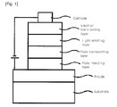
- FIG. 1 illustrates the structure of the organic light emitting device according to one embodiment of the present invention.
- the present invention provides a diamine derivative, represented by Formula 2.
- L1, L2, Ar1, Ar2, Ar3 and Ar4 are the same as defined in claim 1.
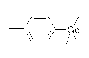
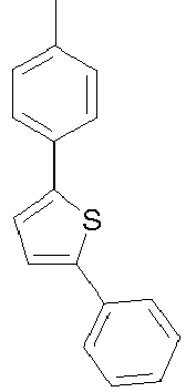
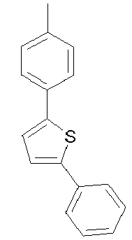
- L1, L2, Ar1, Ar2, Ar3 and Ar4 in Formula 2 are illustrated in the following Table 1.
- the diamine derivative according to the present invention can be prepared by reacting a dibromoaryl compound with an arylamine compound in the presence of a palladium catalyst.
- a specific preparation method will be described in the following Preparation Examples.
- the present invention provides an organic electronic device comprising the diamine derivative represented by Formula 2.
- the diamine derivative according to the present invention can serve as a hole injecting, hole transporting, electron injecting, electron transporting, or light emitting material in an organic electronic device including an organic light emitting device. Particularly, it can serve as a light emitting dopant as used alone, in particular, a blue light emitting dopant.
- the organic electronic device according to the present invention exhibits excellent characteristics in terms of efficiency, drive voltage, life time, and stability.
- the organic electronic device of the present invention can be prepared by usual methods and materials for preparing an organic electronic device, except that the above-described compounds are used to form at least one organic material layer.
- the above-described compounds can serve as a hole injecting, hole transporting, electron injecting, electron transporting, or light emitting material, and particularly serve as a light emitting material as used alone, as well as a light emitting host with an appropriate light emitting dopant or a light emitting dopant with an appropriate light emitting host.
- the organic light emitting device may have a structure that comprises a first electrode, a second electrode and organic material layers interposed therebetween, and can be prepared by usual methods and materials for preparing an organic light emitting device, except that the above-described compound according to the present invention is used to form at least one of the organic material layers in an organic light emitting device.
- the structure of the organic light emitting device according to the present invention is shown in FIG. 1 .
- the organic light emitting device can be prepared by depositing a metal, a metal oxide having conductivity or an alloy thereof on a substrate using a PVD (physical vapor deposition) process such as sputtering and e-beam evaporation to form an anode; forming an organic material layer comprising a hole injecting layer, a hole transporting layer, a light emitting layer, and an electron transporting layer on the anode; and depositing a material, which can be used as a cathode, thereon.
- the organic light emitting device can be prepared by sequentially depositing a cathode material, an organic material layer, and an anode material on a substrate.
- the organic material layer may be of a multilayer structure containing a hole injecting layer, a hole transporting layer, a light emitting layer, an electron transporting layer, and the like, but not limited thereto, and may be of a monolayer structure. Further, the organic material layer can be produced to have a fewer number of layers, by using a variety of polymeric materials, by means of a solvent process rather than a deposit process, such as spin coating, dip coating, doctor blading, screen printing, ink jet printing, and heat transfer processes.
- the anode material is preferably a material having a large work function to facilitate hole injection usually to an organic material layer.
- Specific examples of the anode material which can be used in the present invention include metals such as vanadium, chromium, copper, zinc and gold, or an alloy thereof; metal oxides such as zinc oxide, indium oxide, indium-tin oxide (ITO), and indium zinc oxide (IZO); a combination of a metal and an oxide such as ZnO:Al and SnO 2 :Sb; conductive polymers such as poly(3-methylthiophene), poly[3,4-(ethylene-1,2-dioxy)thiophene] (PEDT), polypyrrole and polyaniline, but not limited thereto.
- the cathode material is preferably a material having a small work function to facilitate electron injection usually to an organic material layer.
- Specific examples of the cathode material include metals such as magnesium, calcium, sodium, potassium, titanium, indium, yttrium, lithium, gadolinium, aluminum, silver, tin and lead, or an alloy thereof; multilayer structure materials such as LiF/Al and LiO 2 /Al, but not limited thereto.
- the hole injecting material is a material facilitating hole injection from an anode at low voltage.
- the HOMO (highest occupied molecular orbital) level of the hole injecting material is preferably located between the work function of the anode materials and the HOMO level of its neighboring organic material layer.
- Specific examples of the hole injecting material include metal porphyrin, oligothiophene, organic materials of arylamine series, hexanitrile hexaazatriphenylene, organic materials of quinacridone series, organic materials of perylene series, anthraquinone, and conductive polymers of polyaniline and polythiophene series, but are not limited thereto.
- the hole transporting material is preferably a material having high hole mobility, which can transfer holes from the anode or the hole injecting layer toward the light emitting layer.
- Specific examples thereof include organic materials of arylamine series, conductive polymers and block copolymers having both conjugated portions and non-conjugated portions, but are not limited thereto.
- the light emitting material are a material capable of emitting visible light by accepting and recombining holes from the hole transporting layer and electrons from the electron transporting layer, preferably a material having high quantum efficiency for fluorescence and phosphorescence.
- Specific examples thereof include 8-hydroxyquinoline aluminum complex (Alq 3 ); compounds of carbazole series; dimerized styryl compounds; BAlq; 10-hydroxybenzoquinoline-metal compounds; compounds of benzoxazole, benzthiazole and benzimidazole series; polymers of poly(p-phenylenevinylene) (PPV) series; spiro compounds; and compounds of polyfluorene and rubrene series, but are not limited thereto.
- PV poly(p-phenylenevinylene)
- the electron transporting material is suitably a material having high electron mobility, which can transfer electrons from the cathode to the light emitting layer.
- a material having high electron mobility which can transfer electrons from the cathode to the light emitting layer.
- Specific examples thereof include 8-hydroxyquinoline aluminum complex; complexes including Alq 3 ; organic radical compounds; and hydroxyflavone-metal complexes, but are not limited thereto.
- the organic light emitting device may be of a front-side, backside or double-sided light emission according to the materials used.
- the compound according to the present invention can function in an organic electronic device including an organic solar cell, an organic photoconductor and an organic transistor, according to a principle similar to that applied to the organic light emitting device.
- the compound of Formula 2 according to the present invention can be prepared in multi-step chemical reactions.
- the preparation of the compound is described by way of Examples below.
- a certain intermediate compound is first prepared, and then the intermediate compound is used to prepare the compound of Formula 2.
- Exemplary intermediate compounds are listed below as Compounds A through Y. In these compounds, Br or Cl may be substituted with any other reactive atoms or functional groups.
- a compound D (3.16 g, 50%) was prepared in the same manner as in Preparation Example 2, except that 1.4-dibromonaphthalene (5 g, 17.5 mmol) was used instead of 1,5-dibromonaphthalene (5 g, 17.5 mmol) in Preparation Example 2.
- MS: [M] 362.
- a compound E (5.9 g, 97%) was prepared in the same manner as in Preparation Example 3, except that 1.4-dibromonaphthalene (5 g, 17.5 mmol) was used instead of 1,5-dibromonaphthalene (5 g, 17.5 mmol) in Preparation Example 3.
- MS: [M] 348.
- a compound F (3.16 g, 50%) was prepared in the same manner as in Preparation Example 2, except that 2.6-dibromonaphthalene (5 g, 17.5 mmol) was used instead of 1,5-dibromonaphthalene (5 g, 17.5 mmol)) in Preparation Example 2.
- MS: [M] 362.
- a compound G (5.9 g, 97%) was prepared in the same manner as in Preparation Example 3, except that 2.6-dibromonaphthalene (5 g, 17.5 mmol) was used instead of 1,5-dibromonaphthalene (5 g, 17.5 mmol) in Preparation Example 3.
- MS: [M] 348.
- the prepared white solid compound (5 g, 31.3 mmol) were dissolved in anhydrous THF (200 mL), and then cooled to -10°C. Then, n-butyllithium (15 mL, 37.5 mmol) was slowly added dropwise, and stirred for 1 hr. Subsequently, the reaction temperature was decreased to -78°C, and then boronic acid trimethylester (10.5 mL, 93.75 mmol) was slowly added, stirred for 12 hrs. After the temperature was decreased to 0°C, a 2 N hydrochloric acid aqueous solution (16 mL) was added thereto, and stirred to obtain a white precipitate.
- the organic layer was extracted with THF, dried over magnesium sulfate, and then filtered under reduced pressure. The filtrate was concentrated to remove the solvent, and the resultant was dissolved in THF. An excessive amount of aqueous solution was added thereto, and the organic layer was separated with dimethylchloromethane. A hydrochloric acid aqueous solution was added to the separated aqueous layer, precipitated, filtered to obtain a compound (2.7 g, 42%).
- a glass substrate (Corning 7059 glass), on which a thin film of ITO (indium tin oxide) was coated to a thickness of 1,000 ⁇ , was immersed in distilled water having a detergent dissolved therein to wash the substrate with ultrasonic waves.
- the detergent as used herein was a product commercially available from Fisher Co. and the distilled water was one which had been twice filtered by using a filter commercially available from Millipore Co.
- ITO was washed for 30 minutes, and then washing with ultrasonic waves was repeated twice for 10 minutes by using distilled water. After the completion of washing with distilled water, washing with ultrasonic waves was carried out by using solvents such as isopropyl alcohol, acetone and methanol.
- solvents such as isopropyl alcohol, acetone and methanol.
- the resultant product was dried, and then transported to a plasma washing machine.
- the substrate was washed for 5 minutes using an oxygen plasma, and then transported to a vacuum depositing machine.
- the compound 2-1 prepared in Comparative Example 1 (2 wt%) was deposited thereon with the following compound Z (300 ⁇ ) to form a light emitting layer, and then 9,10-bis-2-naphthyl-2- [4-(N-phenylbenzoimidazoyl)phenyl] anthracene (300 ⁇ ) was coated by thermal vacuum deposition to form an electron transporting layer.
- Lithium fluoride (LiF) and aluminum were sequentially deposited on the electron transporting layer to thicknesses of 12 ⁇ and 2,000 ⁇ , respectively, to form a cathode, thereby obtaining an organic light emitting device.
- the deposition rate of the organic material was maintained at 0.4 to 0.7 ⁇ /sec and the deposition rate of lithium fluoride on the cathode was maintained at 0.3 ⁇ /sec and the deposition rate of aluminum was maintained at 2 ⁇ /sec.
- the degree of vacuum upon deposition was maintained at 2 ⁇ 10 -7 to 5 ⁇ 10 -18 torr.
- An organic light emitting device was prepared in the same manner as in Comparative Experimental Example 1, except that the compound 2-68 prepared in Comparative Example 8 was used instead of the compound 2-1 in Comparative Experimental Example 1.
- An organic light emitting device was prepared in the same manner as in Comparative Experimental Example 1, except that the compound 2-70 prepared in Comparative Example 9 was used instead of the compound 2-1 in Comparative Experimental Example 1.
- An organic light emitting device was prepared in the same manner as in Comparative Experimental Example 1, except that the compound 2-119 prepared in Example 15 was used instead of the compound 2-1 in Comparative Experimental Example 1.
- An organic light emitting device was prepared in the same manner as in Comparative Experimental Example 1, except that the compound 2-121 prepared in Example 16 was used instead of the compound 2-1 in Comparative Experimental Example 1.
- An organic light emitting device was prepared in the same manner as in Comparative Experimental Example 1, except that the compound 2-179 prepared in Example 21 was used instead of the compound 2-1 in Comparative Experimental Example 1.
- HAT hexanitrile hexaazatriphenylene
- the compound 2-52 (400 ⁇ ) prepared in Comparative Example 4 was vacuum-deposited to form a hole transporting layer.
- Alq 3 was vacuum-deposited to a thickness of 300 ⁇ , thus to form a light emitting layer.
- the electron transporting layer material of the following Formula was deposited to a thickness of 200 ⁇ , thus to form an electron transporting layer.
- lithium fluoride (LiF) and aluminum were sequentially vacuum-deposited to a thickness of 12 ⁇ and 2,000 ⁇ , respectively, to form a cathode.
- the deposition rate of the organic material was maintained at 0.3 to 0.8 ⁇ /sec and the deposition rates of lithium fluoride and aluminum of the cathode were maintained at 0.3 ⁇ /sec and 1.5 to 2.5 ⁇ /sec, respectively.
- the vacuum degree during deposition was maintained at 1 x 10 -7 ⁇ 3 ⁇ 10 -7 torr.
- An organic light emitting device was prepared in the same manner as in Comparative Experimental Example 7, except that the compound 3-78 prepared in Comparative Example 11 was used instead of the compound 2-52 used as a hole transporting layer in Comparative Experimental Example 7.
- An organic light emitting device was prepared in the same manner as in Comparative Experimental Example 7, except that the compound 4-78 prepared in Comparative Example 12 was used instead of the compound 2-52 used as a hole transporting layer in Comparative Experimental Example 7.
- An organic light emitting device was prepared in the same manner as in Comparative Experimental Example 7, except that the compound 2-104 prepared in Example 13 was used instead of the compound 2-52 used as a hole transporting layer in Comparative Experimental Example 7.
- An organic light emitting device was prepared in the same manner as in Comparative Experimental Example 7, except that the compound 2-113 prepared in Example 14 was used instead of the compound 2-52 used as a hole transporting layer in Comparative Experimental Example 7.
- An organic light emitting device was prepared in the same manner as in Comparative Experimental Example 7, except that the compound 2-125 prepared in Example 17 was used instead of the compound 2-52 used as a hole transporting layer in Comparative Experimental Example 7.
- An organic light emitting device was prepared in the same manner as in Comparative Experimental Example 7, except that the compound 2-127 prepared in Example 18 was used instead of the compound 2-52 used as a hole transporting layer in Comparative Experimental Example 7.
- An organic light emitting device was prepared in the same manner as in Comparative Experimental Example 7, except that the compound 2-131 prepared in Example 19 was used instead of the compound 2-52 used as a hole transporting layer in Comparative Experimental Example 7.
- An organic light emitting device was prepared in the same manner as in Comparative Experimental Example 7, except that the compound 2-155 prepared in Example 20 was used instead of the compound 2-52 used as a hole transporting layer in Comparative Experimental Example 7.
- An organic light emitting device was prepared in the same manner as in Comparative Experimental Example 7, except that a commercial NPB material of the following Formula (see EP 0 924 192 ) was used instead of the compound 2-52 used as a hole transporting layer in Comparative Experimental Example 7.
- the diamine derivative according to the present invention was found to exhibit effects of lower operating voltage and increased efficiency of an organic electronic device.
Landscapes
- Chemical & Material Sciences (AREA)
- Organic Chemistry (AREA)
- Engineering & Computer Science (AREA)
- Materials Engineering (AREA)
- Physics & Mathematics (AREA)
- Spectroscopy & Molecular Physics (AREA)
- Electroluminescent Light Sources (AREA)
- Organic Low-Molecular-Weight Compounds And Preparation Thereof (AREA)
- Heterocyclic Compounds Containing Sulfur Atoms (AREA)
- Nitrogen Condensed Heterocyclic Rings (AREA)
Claims (9)
- Diaminderivat, dargestellt durch die folgende Formel 2:
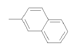
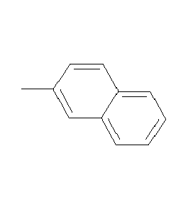
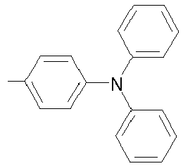
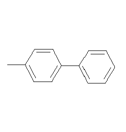
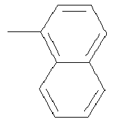
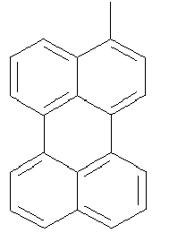
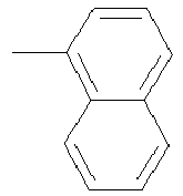
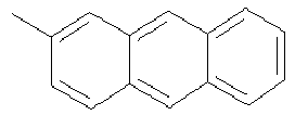
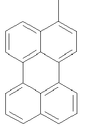
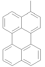
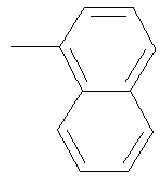
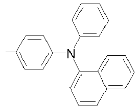
 wobei L1 und L2 gleich oder verschieden voneinander sind und jeweils unabhängig voneinander ausgewählt sind aus der Gruppe bestehend aus einer unsubstituierten Phenylengruppe und einer unsubstituierten Naphthylengruppe;wobei Ar1 und Ar3 der Formel 2 gleich oder verschieden voneinander sind und jeweils unabhängig ausgewählt sind aus der Gruppe bestehend aus einer Phenylgruppe, einer Biphenylgruppe, einer Naphthylgruppe und einer Phenylgruppe substituiert mit -SiRR'R" oder -GeRR'R", wobei R, R' und R" gleich oder verschieden voneinander sind und jeweils unabhängig Wasserstoff, eine C1-C20-Alkylgruppe, eine C3-C20-Cycloalkylgruppe, eine C6-C20-Arylgruppe oder eine heterocyclische C5-C20-Gruppe sind,wobei Ar2 und Ar4 der Formel 2 gleich oder verschieden voneinander sind und jeweils unabhängig ausgewählt sind aus der Gruppe bestehend aus einer Phenylgruppe; einer Biphenylgruppe; einer Naphthylgruppe; einer Anthracenylgruppe; einer Pyrenylgruppe; einer Perylenylgruppe; einer Phenylgruppe substituiert mit SiRR'R", -GeRR'R", einer C6-C20-Arylamingruppe oder einer C6-C20-Arylgruppe; und den folgenden Substituenten:
 wobei R, R' und R" gleich oder verschieden voneinander sind und jeweils unabhängig Wasserstoff, eine C1-C20-Alkylgruppe, eine C3-C20-Cycloalkylgruppe, eine C6-C20-Arylgruppe oder eine heterocyclische C5-C2o-Gruppe sind,wobei im Falle, dass Ar2 und Ar4 ausgewählt sind aus den folgenden Substituenten Ar2 das gleiche wie Ar4 ist; L1 das gleiche ist wie L2, und L1 und L2 eine unsubstituierte Phenylengruppe oder eine unsubstituierte Naphthylengruppe sind, und Ar1 das gleiche ist wie Ar3, und Ar1 und Ar3 eine unsubstituierte Phenylgruppe oder eine unsubstituierte Naphthylgruppe sind:

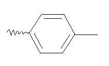
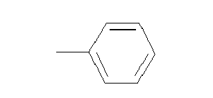
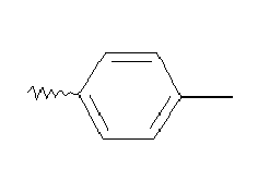
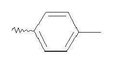
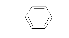
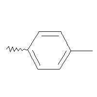
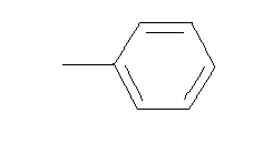
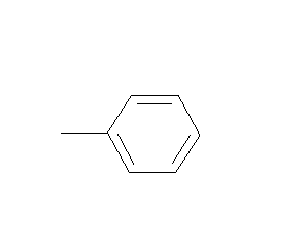
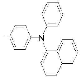
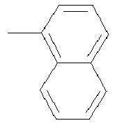
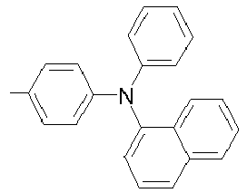
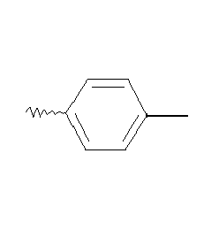
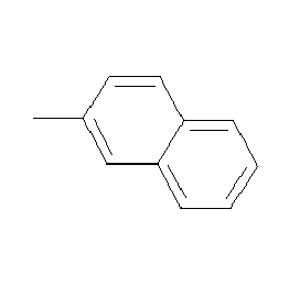
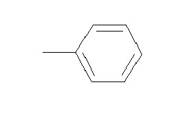
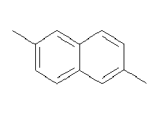
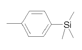
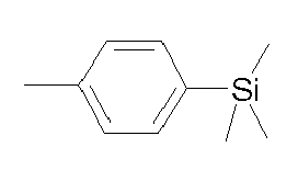
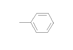
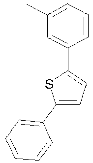
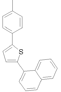
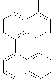
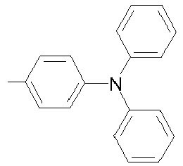
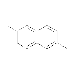
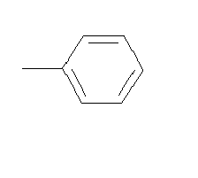
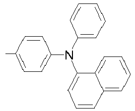
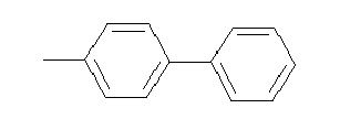
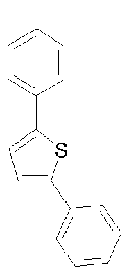
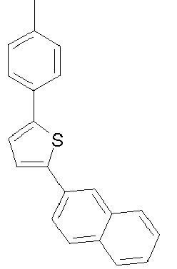
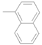
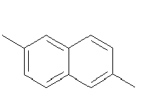
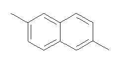
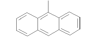
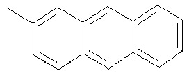
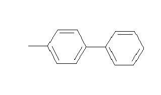
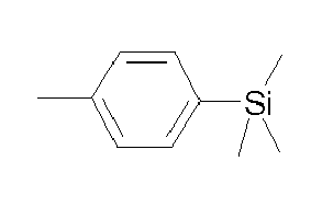
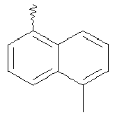
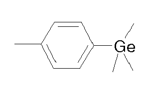
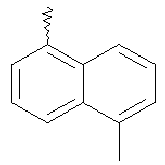
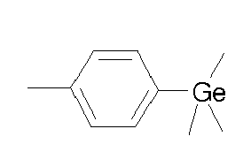
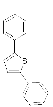
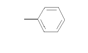
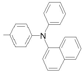
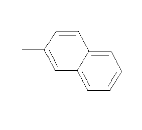
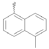
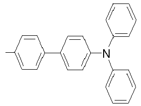
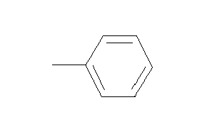
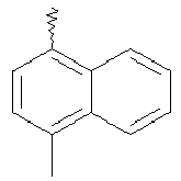
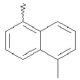
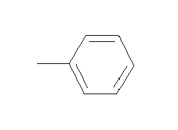
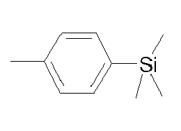
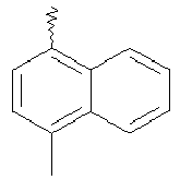
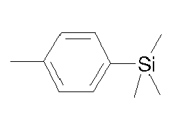
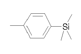
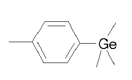
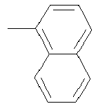
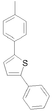
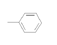
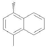
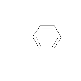
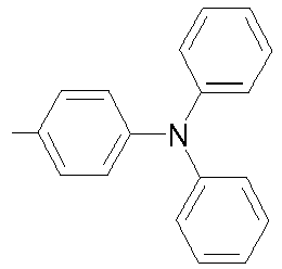
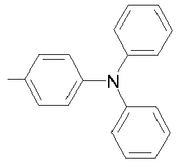
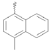
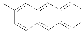
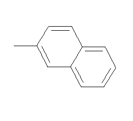
- Diaminderivat nach Anspruch 1, wobei L1, L2, Ar1, Ar2, Ar3 und Ar4 der Formel 2 ausgewählt sind aus den Gruppen der folgenden Tabelle 1:
[Tabelle 1] L1 L2 Ar1 Ar2 Ar3 Ar4 101 
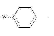

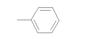
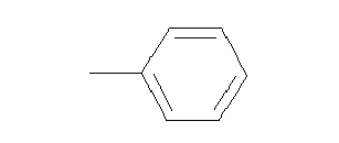

102 


103 



104 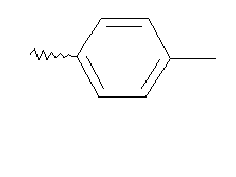


105 


106 


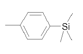
107 


108 


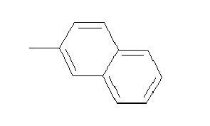


109 


110 


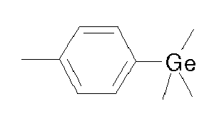

111 


112 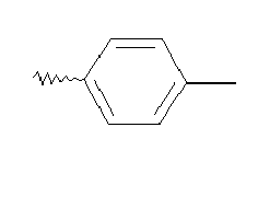



113 


115 



116 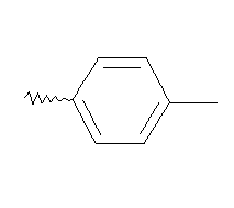


117 


118 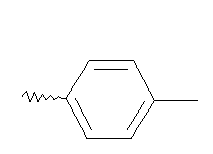


119 


120 



121 

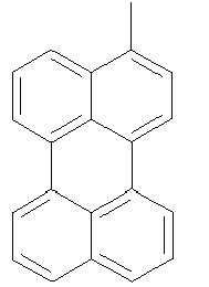
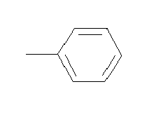
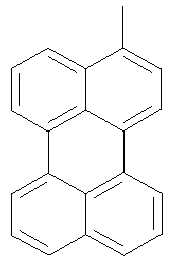
122 


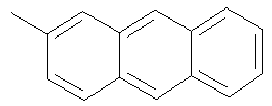

123 


124 


125 


126 


127 


128 


129 


131 


132 



133 
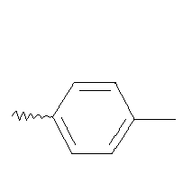


134 


135 


136 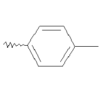


137 

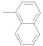


138 


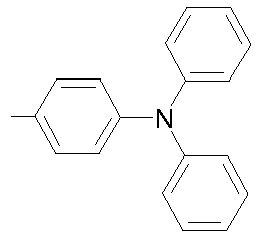


139 


140 


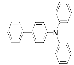


142 


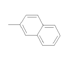

143 

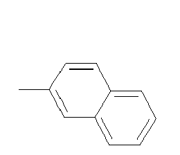


144 


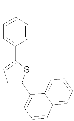


145 


146 



147 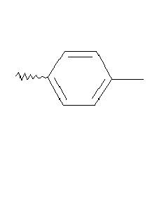


148 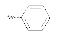


149 


150 


151 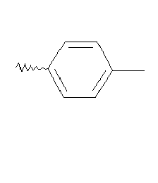



152 


153 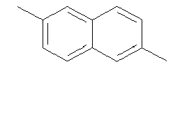



154 


155 


156 



157 


158 


159 



160 


161 


162 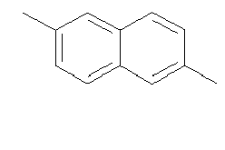


163 


165 



166 




167 


168 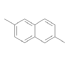




169 


170 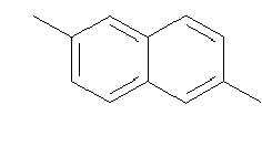


171 




172 


173 


174 



175 


176 


177 


178 


179 


181 


182 


183 



184 


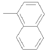

185 


186 


187 


188 


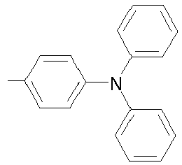


189 


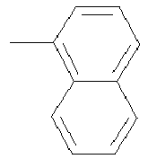

190 


192 


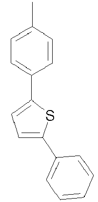


193 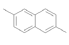


194 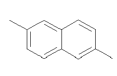


195 


196 


197 


198 




199 


200 


201 


202 


203 


204 


205 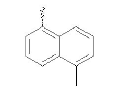




206 



207 


208 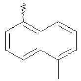


209 


210 



211 


212 


213 



215 



216 


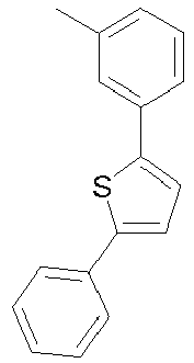
217 
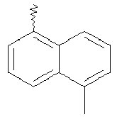


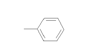

218 
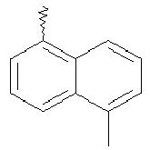


219 


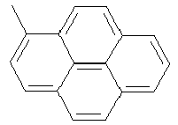
220 


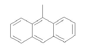


221 


222 


223 


224 
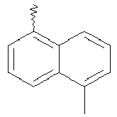


225 


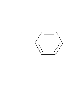

226 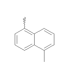




227 


228 



229 


231 



232 
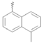


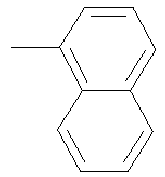
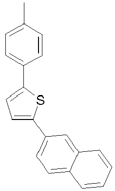
233 


234 


235 
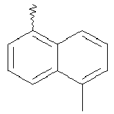


236 




237 



238 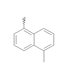


239 


240 


242 


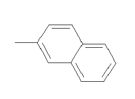

243 
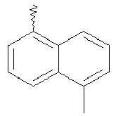


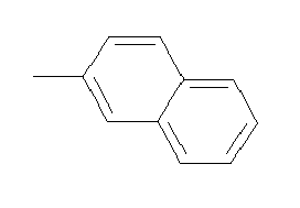
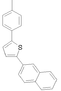
244 
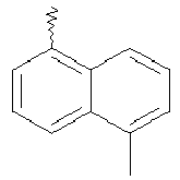


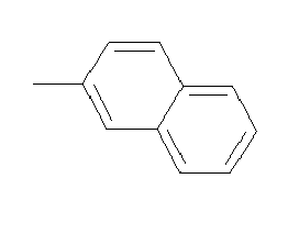

245 


246 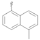


247 

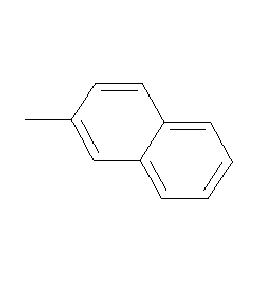


248 
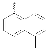
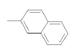
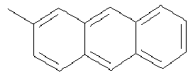


249 


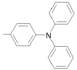
250 



251 



252 



253 


254 



255 


256 



257 


258 


259 



260 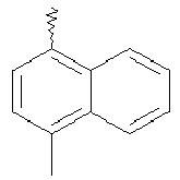


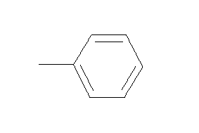
261 


262 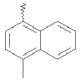


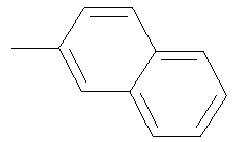


263 



265 




266 


267 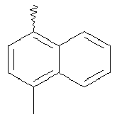


268 

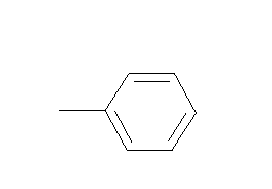


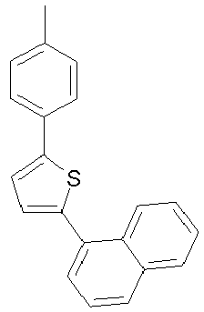
269 

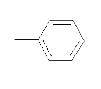


270 


271 


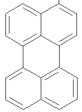

272 



273 

274 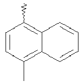


275 


276 


277 


278 


279 


281 


282 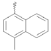


283 


284 


285 


286 




287 



288 


289 


290 


292 


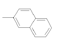

293 

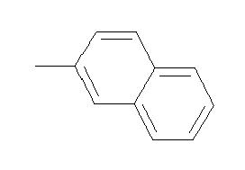


294 


295 


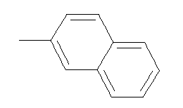

296 
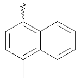

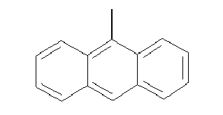
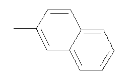

297 


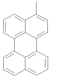


298 

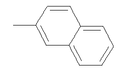


299 


300 



301 


- Organisches elektronisches Bauelement umfassend eine erste Elektrode, eine zweite Elektrode und eine oder mehrere organische Materialschichten, die dazwischen angeordnet sind, wobei wenigstens eine organische Materialschicht das Diamindeuvat nach einem der Ansprüche 1 bis 2 umfasst.
- Organisches elektronisches Bauelement nach Anspruch 3, wobei das organische elektronische Bauelement eine normale Struktur aufweist, hergestellt durch nacheinander folgendes Laminieren einer Anode, einer oder mehrerer organischer Materialschichten und einer Kathode auf einem Substrat.
- Organisches elektronisches Bauelement nach Anspruch 3, wobei das organische elektronische Bauelement eine invertierte Struktur aufweist, hergestellt durch nacheinander folgendes Laminieren einer Kathode, einer oder mehrerer organischer Materialschichten und einer Anode auf einem Substrat.
- Organisches elektronisches Bauelement nach Anspruch 3, wobei die organische Materialschicht wenigstens eines einer Lochinjektionsschicht, einer Lochtransportschicht und einer Lochinjektions- und Lochtransportschicht umfasst und wenigstens eine der Schichten das Diaminderivat der Formel 2 umfasst.
- Organisches elektronisches Bauelement nach Anspruch 3, wobei die organische Materialschicht eine lichtemittierende Schicht umfasst und die lichtemittierende Schicht das Diaminderivat der Formel 2 umfasst.
- Organisches elektronisches Bauelement nach Anspruch 3, wobei die organische Materialschicht eine Elektronentransportschicht umfasst und die Elektronentransportschicht das Diaminderivat der Formel 2 umfasst.
- Organisches elektronisches Bauelement nach Anspruch 3, wobei das organische elektronische Bauelement ausgewählt ist aus der Gruppe bestehend aus einem organischen lichtemittierenden Bauelement, einer organischen Photovoltaikzelle, einem organischen Photoleiter (OPC) und einem organischen Transistor.
Applications Claiming Priority (2)
| Application Number | Priority Date | Filing Date | Title |
|---|---|---|---|
| KR20070040965 | 2007-04-26 | ||
| PCT/KR2008/002380 WO2008133459A1 (en) | 2007-04-26 | 2008-04-25 | New diamine derivatives and organic electronic device using the same |
Publications (3)
| Publication Number | Publication Date |
|---|---|
| EP2139846A1 EP2139846A1 (de) | 2010-01-06 |
| EP2139846A4 EP2139846A4 (de) | 2011-08-24 |
| EP2139846B1 true EP2139846B1 (de) | 2016-09-07 |
Family
ID=39925857
Family Applications (1)
| Application Number | Title | Priority Date | Filing Date |
|---|---|---|---|
| EP08753194.3A Active EP2139846B1 (de) | 2007-04-26 | 2008-04-25 | Neue diaminderivate und diese verwendende organische elektronische vorrichtung |
Country Status (7)
| Country | Link |
|---|---|
| US (1) | US8026514B2 (de) |
| EP (1) | EP2139846B1 (de) |
| JP (2) | JP5373769B2 (de) |
| KR (1) | KR101012578B1 (de) |
| CN (1) | CN101668730B (de) |
| TW (1) | TWI478898B (de) |
| WO (1) | WO2008133459A1 (de) |
Cited By (1)
| Publication number | Priority date | Publication date | Assignee | Title |
|---|---|---|---|---|
| US11968887B2 (en) | 2019-11-27 | 2024-04-23 | Samsung Display Co., Ltd. | Organic electroluminescence device and diamine compound for organic electroluminescence device |
Families Citing this family (16)
| Publication number | Priority date | Publication date | Assignee | Title |
|---|---|---|---|---|
| WO2008133459A1 (en) * | 2007-04-26 | 2008-11-06 | Lg Chem, Ltd. | New diamine derivatives and organic electronic device using the same |
| KR20100070979A (ko) * | 2008-12-18 | 2010-06-28 | 동우 화인켐 주식회사 | 비대칭 구조의 유기전기발광소자용 아릴아민유도체, 그 제조방법, 이를 포함하는 유기전기발광소자용 유기박막재료 및 이를 이용한 유기 전기발광소자 |
| TWI402243B (zh) * | 2010-01-06 | 2013-07-21 | 國立交通大學 | 有機發光材料 |
| EP2776386B1 (de) * | 2011-11-11 | 2019-11-20 | Merck Patent GmbH | Verfahren zur herstellung von arylaminen |
| US9130172B2 (en) * | 2012-05-08 | 2015-09-08 | Arizona Board Of Regents, A Body Corporate Of The State Of Arizona Acting For And On Behalf Of Arizona State University | Naphthyl-containing compounds for light-emitting devices |
| KR102105076B1 (ko) | 2013-06-04 | 2020-04-28 | 삼성디스플레이 주식회사 | 축합환 화합물 및 이를 포함하는 유기 전계 발광 소자 |
| JP6012889B2 (ja) | 2014-09-19 | 2016-10-25 | 出光興産株式会社 | 新規な化合物 |
| TWI672358B (zh) * | 2017-06-20 | 2019-09-21 | 南韓商Lg化學股份有限公司 | 化合物、包括其之塗覆組成物與包括其之有機發光裝置 |
| WO2018236146A1 (ko) * | 2017-06-20 | 2018-12-27 | 주식회사 엘지화학 | 화합물, 이를 포함하는 코팅조성물 및 이를 포함한 유기 발광 소자 |
| KR102608415B1 (ko) | 2018-04-27 | 2023-12-01 | 삼성디스플레이 주식회사 | 다이아민 화합물을 포함한 유기 발광 소자 및 다이아민 화합물 |
| KR102630639B1 (ko) | 2018-06-20 | 2024-01-30 | 삼성디스플레이 주식회사 | 다이아민 화합물을 포함한 유기 발광 소자 및 다이아민 화합물 |
| CN112142605B (zh) * | 2019-06-28 | 2024-03-12 | 北京鼎材科技有限公司 | 一种化合物及其应用、包含其的有机电致发光器件 |
| CN114516804B (zh) * | 2020-11-18 | 2024-10-22 | 江苏三月科技股份有限公司 | 一种二胺衍生物及使用该衍生物的有机电致发光器件 |
| KR102526084B1 (ko) * | 2022-02-25 | 2023-04-26 | 주식회사 코스텔코리아 | 유기 광전도성 재료 및 이를 이용한 광변환 소자 |
| CN116217410B (zh) * | 2023-02-22 | 2025-05-27 | 长春海谱润斯科技股份有限公司 | 一种双胺衍生物及其有机电致发光器件 |
| CN117143140B (zh) * | 2023-09-06 | 2026-05-15 | 长春海谱润斯科技股份有限公司 | 一种三芳胺类化合物及其有机电致发光器件 |
Family Cites Families (33)
| Publication number | Priority date | Publication date | Assignee | Title |
|---|---|---|---|---|
| US535878A (en) * | 1895-03-19 | Watering-trough | ||
| JPH0789225B2 (ja) * | 1986-02-28 | 1995-09-27 | キヤノン株式会社 | 電子写真感光体 |
| JPH0586009A (ja) * | 1991-09-24 | 1993-04-06 | Mita Ind Co Ltd | アゾ系化合物およびジアゾニウム塩 |
| US5358788A (en) | 1992-04-02 | 1994-10-25 | Idemitsu Kosan Company Limited | Organic electroluminescence device containing a silanamine compound |
| US5985417A (en) * | 1996-09-03 | 1999-11-16 | Motorola, Inc. | Polymer stabilized molecular whole transporting materials for organic electroluminescence displays |
| JP3633236B2 (ja) * | 1997-10-06 | 2005-03-30 | 東洋インキ製造株式会社 | 有機エレクトロルミネッセンス素子材料およびそれを使用した有機エレクトロルミネッセンス素子 |
| JP3985311B2 (ja) * | 1997-10-20 | 2007-10-03 | チッソ株式会社 | アミン誘導体及びそれを用いた有機電界発光素子 |
| US6468675B1 (en) | 1998-05-29 | 2002-10-22 | Nec Corporation | Organic electroluminescent device having high luminance efficiency |
| KR100869622B1 (ko) * | 1998-12-28 | 2008-11-21 | 이데미쓰 고산 가부시키가이샤 | 유기 전기발광 소자용 재료 및 이를 포함하는 유기전기발광 소자 |
| JP4799717B2 (ja) * | 1999-05-24 | 2011-10-26 | 三井化学株式会社 | アミン化合物 |
| EP1347031A4 (de) * | 2000-09-07 | 2007-07-04 | Idemitsu Kosan Co | Organisches elektrolumineszierendes element |
| US6468575B2 (en) * | 2001-02-05 | 2002-10-22 | Fremont Beef Company | Method for molding and shaping tongue |
| JP4477802B2 (ja) * | 2001-09-17 | 2010-06-09 | 三井化学株式会社 | アミン化合物および該化合物を含有する有機電界発光素子 |
| JP4477803B2 (ja) * | 2001-09-19 | 2010-06-09 | 三井化学株式会社 | アミン化合物および該化合物を含有する有機電界発光素子 |
| US6849345B2 (en) | 2001-09-28 | 2005-02-01 | Eastman Kodak Company | Organic electroluminescent devices with high luminance |
| US20030118666A1 (en) * | 2001-10-12 | 2003-06-26 | Seiji Nishida | Injectable solution containing a shark-derived chondroitin sulfate iron colloid |
| JP3823312B2 (ja) * | 2001-10-18 | 2006-09-20 | 日本電気株式会社 | 有機薄膜トランジスタ |
| KR100577179B1 (ko) * | 2001-10-30 | 2006-05-10 | 엘지전자 주식회사 | 유기 전계 발광 소자 |
| EP2295519B1 (de) * | 2002-07-19 | 2016-05-18 | Idemitsu Kosan Co., Ltd. | Organische elektrolumineszente vorrichtungen und organisches lichtemittierendes medium |
| JP4424026B2 (ja) * | 2003-04-07 | 2010-03-03 | 三菱化学株式会社 | 2,7−ジアミノナフタレン化合物、電荷輸送材料、有機電界発光素子材料、および有機電界発光素子 |
| JP4415582B2 (ja) * | 2003-07-02 | 2010-02-17 | 三菱化学株式会社 | 有機電界発光素子およびその製造方法 |
| JP2006100756A (ja) * | 2003-11-07 | 2006-04-13 | Sony Corp | 有機電界発光素子および表示装置 |
| JP2005145010A (ja) * | 2003-11-19 | 2005-06-09 | Mitsui Chemicals Inc | 光記録媒体 |
| JP2005169782A (ja) * | 2003-12-10 | 2005-06-30 | Mitsui Chemicals Inc | 光記録媒体 |
| US20060021647A1 (en) * | 2004-07-28 | 2006-02-02 | Gui John Y | Molecular photovoltaics, method of manufacture and articles derived therefrom |
| US7100385B2 (en) * | 2004-08-03 | 2006-09-05 | Lucent Technologies Inc. | Thermal management system for electrical enclosures |
| US20060141287A1 (en) * | 2004-08-19 | 2006-06-29 | Eastman Kodak Company | OLEDs with improved operational lifetime |
| KR100670185B1 (ko) | 2004-12-30 | 2007-02-28 | 한국화인케미칼주식회사 | 1,5-디아미노나프탈렌 유도체 및 그 제조방법, 그 제조용조성물, 그를 포함하는 유기전계 발광소자 |
| JP5201798B2 (ja) * | 2005-03-22 | 2013-06-05 | 株式会社半導体エネルギー研究所 | 液晶表示装置 |
| US20060269781A1 (en) * | 2005-05-24 | 2006-11-30 | Jun-Liang Lai | Diarylamino substituted compounds and an electroluminescent device having the compounds |
| CN101405255B (zh) * | 2006-03-23 | 2013-01-30 | Lg化学株式会社 | 新的二胺衍生物、其制备方法以及使用该二胺衍生物的有机电子器件 |
| JP5319287B2 (ja) * | 2006-09-22 | 2013-10-16 | 出光興産株式会社 | 芳香族アミン誘導体及びそれを用いた有機エレクトロルミネッセンス素子 |
| WO2008133459A1 (en) * | 2007-04-26 | 2008-11-06 | Lg Chem, Ltd. | New diamine derivatives and organic electronic device using the same |
-
2008
- 2008-04-25 WO PCT/KR2008/002380 patent/WO2008133459A1/en not_active Ceased
- 2008-04-25 JP JP2010506071A patent/JP5373769B2/ja active Active
- 2008-04-25 CN CN200880013651.7A patent/CN101668730B/zh active Active
- 2008-04-25 US US12/451,063 patent/US8026514B2/en active Active
- 2008-04-25 KR KR1020080038606A patent/KR101012578B1/ko active Active
- 2008-04-25 EP EP08753194.3A patent/EP2139846B1/de active Active
- 2008-04-25 TW TW097115314A patent/TWI478898B/zh active
-
2013
- 2013-07-12 JP JP2013146866A patent/JP2014005283A/ja active Pending
Non-Patent Citations (1)
| Title |
|---|
| BELLMANN: "New Triarylamine-Containing Polymers as Hole Transport Materials in Organic Light-Emitting Diodes: Effect of Polymer Structure and Cross-Linking on Device Characteristics", 30 April 1998 (1998-04-30), XP055030500, Retrieved from the Internet <URL:http://pubs.acs.org/doi/pdf/10.1021/cm980030p> [retrieved on 20120620] * |
Cited By (1)
| Publication number | Priority date | Publication date | Assignee | Title |
|---|---|---|---|---|
| US11968887B2 (en) | 2019-11-27 | 2024-04-23 | Samsung Display Co., Ltd. | Organic electroluminescence device and diamine compound for organic electroluminescence device |
Also Published As
| Publication number | Publication date |
|---|---|
| EP2139846A1 (de) | 2010-01-06 |
| CN101668730A (zh) | 2010-03-10 |
| KR101012578B1 (ko) | 2011-02-07 |
| TW200904782A (en) | 2009-02-01 |
| CN101668730B (zh) | 2016-09-21 |
| US8026514B2 (en) | 2011-09-27 |
| JP2010525054A (ja) | 2010-07-22 |
| TWI478898B (zh) | 2015-04-01 |
| KR20080096440A (ko) | 2008-10-30 |
| US20100187504A1 (en) | 2010-07-29 |
| WO2008133459A1 (en) | 2008-11-06 |
| EP2139846A4 (de) | 2011-08-24 |
| JP2014005283A (ja) | 2014-01-16 |
| JP5373769B2 (ja) | 2013-12-18 |
Similar Documents
| Publication | Publication Date | Title |
|---|---|---|
| EP1902013B1 (de) | Neue antracen-derivate, prozesse für ihre herstellung und ihre verwendung für organische lichtemittierende anzeigen | |
| EP1996540B1 (de) | Neue diaminderivate, verfahren zu deren herstellung und organisches elektronisches gerät, bei dem diese verwendet werden | |
| US8026514B2 (en) | Diamine derivatives and organic electronic device using the same | |
| US8173273B2 (en) | Anthracene derivatives, method for preparation thereof, and organic electronic device using the same | |
| EP1828343B1 (de) | Pyrenderivate und pyrenderivate verwendende organische elektronische vorrichtung | |
| EP2364964B1 (de) | Neuartiges Anthrazenderivat und organische elektronische Vorrichtung damit | |
| EP1976814B1 (de) | Neue anthracenderivate, herstellungsverfahren dafür und diese verwendende organische leuchtdiode | |
| WO2008013399A1 (en) | Anthracene derivatives, organic electronic devices using anthracene derivatives, and electronic apparatuses comprising organic electronic device | |
| CN101238194B (zh) | 茚衍生物以及使用该衍生物的有机发光二极管 | |
| KR101273057B1 (ko) | 신규한 안트라센 유도체 및 이를 이용한 유기 전자 소자 | |
| KR20090052697A (ko) | 신규한 안트라센 유도체 및 이를 이용한 유기 전자 소자 |
Legal Events
| Date | Code | Title | Description |
|---|---|---|---|
| PUAI | Public reference made under article 153(3) epc to a published international application that has entered the european phase |
Free format text: ORIGINAL CODE: 0009012 |
|
| 17P | Request for examination filed |
Effective date: 20091021 |
|
| AK | Designated contracting states |
Kind code of ref document: A1 Designated state(s): AT BE BG CH CY CZ DE DK EE ES FI FR GB GR HR HU IE IS IT LI LT LU LV MC MT NL NO PL PT RO SE SI SK TR |
|
| RIN1 | Information on inventor provided before grant (corrected) |
Inventor name: KIM, JI-EUN Inventor name: JEON, BYUNG-SUN Inventor name: KIM, SEONG-SO Inventor name: KIM, EUN-JU Inventor name: PARK, TAE-YOON Inventor name: KIM, KONG-KYEOM Inventor name: CHO, WOOK-DONG Inventor name: JANG, HYE-YOUNG Inventor name: BAE, JAE-SOON Inventor name: PARK, JIN-KYOON Inventor name: LEE, JAE-CHOL |
|
| DAX | Request for extension of the european patent (deleted) | ||
| A4 | Supplementary search report drawn up and despatched |
Effective date: 20110722 |
|
| RIC1 | Information provided on ipc code assigned before grant |
Ipc: C07C 211/50 20060101AFI20110718BHEP |
|
| 17Q | First examination report despatched |
Effective date: 20120605 |
|
| REG | Reference to a national code |
Ref country code: DE Ref legal event code: R079 Ref document number: 602008046138 Country of ref document: DE Free format text: PREVIOUS MAIN CLASS: C07C0211500000 Ipc: C07C0211540000 |
|
| RIC1 | Information provided on ipc code assigned before grant |
Ipc: C07D 333/20 20060101ALI20150413BHEP Ipc: H01L 51/50 20060101ALI20150413BHEP Ipc: C07C 211/58 20060101ALI20150413BHEP Ipc: C07C 211/54 20060101AFI20150413BHEP Ipc: C07C 211/61 20060101ALI20150413BHEP |
|
| GRAP | Despatch of communication of intention to grant a patent |
Free format text: ORIGINAL CODE: EPIDOSNIGR1 |
|
| INTG | Intention to grant announced |
Effective date: 20160613 |
|
| RIN1 | Information on inventor provided before grant (corrected) |
Inventor name: PARK, JIN-KYOON Inventor name: JEON, BYUNG-SUN Inventor name: KIM, JI-EUN Inventor name: CHO, WOOK-DONG Inventor name: LEE, JAE-CHOL Inventor name: BAE, JAE-SOON Inventor name: KIM, KONG-KYEOM Inventor name: JANG, HYE-YOUNG Inventor name: KIM, SEONG-SO Inventor name: KIM, EUN-JU Inventor name: PARK, TAE-YOON |
|
| GRAS | Grant fee paid |
Free format text: ORIGINAL CODE: EPIDOSNIGR3 |
|
| GRAA | (expected) grant |
Free format text: ORIGINAL CODE: 0009210 |
|
| AK | Designated contracting states |
Kind code of ref document: B1 Designated state(s): AT BE BG CH CY CZ DE DK EE ES FI FR GB GR HR HU IE IS IT LI LT LU LV MC MT NL NO PL PT RO SE SI SK TR |
|
| REG | Reference to a national code |
Ref country code: GB Ref legal event code: FG4D |
|
| REG | Reference to a national code |
Ref country code: CH Ref legal event code: EP |
|
| REG | Reference to a national code |
Ref country code: IE Ref legal event code: FG4D |
|
| REG | Reference to a national code |
Ref country code: AT Ref legal event code: REF Ref document number: 826702 Country of ref document: AT Kind code of ref document: T Effective date: 20161015 |
|
| REG | Reference to a national code |
Ref country code: DE Ref legal event code: R096 Ref document number: 602008046138 Country of ref document: DE |
|
| REG | Reference to a national code |
Ref country code: LT Ref legal event code: MG4D |
|
| REG | Reference to a national code |
Ref country code: NL Ref legal event code: MP Effective date: 20160907 |
|
| PG25 | Lapsed in a contracting state [announced via postgrant information from national office to epo] |
Ref country code: NO Free format text: LAPSE BECAUSE OF FAILURE TO SUBMIT A TRANSLATION OF THE DESCRIPTION OR TO PAY THE FEE WITHIN THE PRESCRIBED TIME-LIMIT Effective date: 20161207 Ref country code: HR Free format text: LAPSE BECAUSE OF FAILURE TO SUBMIT A TRANSLATION OF THE DESCRIPTION OR TO PAY THE FEE WITHIN THE PRESCRIBED TIME-LIMIT Effective date: 20160907 Ref country code: LT Free format text: LAPSE BECAUSE OF FAILURE TO SUBMIT A TRANSLATION OF THE DESCRIPTION OR TO PAY THE FEE WITHIN THE PRESCRIBED TIME-LIMIT Effective date: 20160907 Ref country code: FI Free format text: LAPSE BECAUSE OF FAILURE TO SUBMIT A TRANSLATION OF THE DESCRIPTION OR TO PAY THE FEE WITHIN THE PRESCRIBED TIME-LIMIT Effective date: 20160907 |
|
| REG | Reference to a national code |
Ref country code: AT Ref legal event code: MK05 Ref document number: 826702 Country of ref document: AT Kind code of ref document: T Effective date: 20160907 |
|
| PG25 | Lapsed in a contracting state [announced via postgrant information from national office to epo] |
Ref country code: ES Free format text: LAPSE BECAUSE OF FAILURE TO SUBMIT A TRANSLATION OF THE DESCRIPTION OR TO PAY THE FEE WITHIN THE PRESCRIBED TIME-LIMIT Effective date: 20160907 Ref country code: SE Free format text: LAPSE BECAUSE OF FAILURE TO SUBMIT A TRANSLATION OF THE DESCRIPTION OR TO PAY THE FEE WITHIN THE PRESCRIBED TIME-LIMIT Effective date: 20160907 Ref country code: LV Free format text: LAPSE BECAUSE OF FAILURE TO SUBMIT A TRANSLATION OF THE DESCRIPTION OR TO PAY THE FEE WITHIN THE PRESCRIBED TIME-LIMIT Effective date: 20160907 Ref country code: NL Free format text: LAPSE BECAUSE OF FAILURE TO SUBMIT A TRANSLATION OF THE DESCRIPTION OR TO PAY THE FEE WITHIN THE PRESCRIBED TIME-LIMIT Effective date: 20160907 Ref country code: GR Free format text: LAPSE BECAUSE OF FAILURE TO SUBMIT A TRANSLATION OF THE DESCRIPTION OR TO PAY THE FEE WITHIN THE PRESCRIBED TIME-LIMIT Effective date: 20161208 |
|
| REG | Reference to a national code |
Ref country code: FR Ref legal event code: PLFP Year of fee payment: 10 |
|
| PG25 | Lapsed in a contracting state [announced via postgrant information from national office to epo] |
Ref country code: RO Free format text: LAPSE BECAUSE OF FAILURE TO SUBMIT A TRANSLATION OF THE DESCRIPTION OR TO PAY THE FEE WITHIN THE PRESCRIBED TIME-LIMIT Effective date: 20160907 Ref country code: EE Free format text: LAPSE BECAUSE OF FAILURE TO SUBMIT A TRANSLATION OF THE DESCRIPTION OR TO PAY THE FEE WITHIN THE PRESCRIBED TIME-LIMIT Effective date: 20160907 |
|
| PG25 | Lapsed in a contracting state [announced via postgrant information from national office to epo] |
Ref country code: BE Free format text: LAPSE BECAUSE OF FAILURE TO SUBMIT A TRANSLATION OF THE DESCRIPTION OR TO PAY THE FEE WITHIN THE PRESCRIBED TIME-LIMIT Effective date: 20160907 Ref country code: PL Free format text: LAPSE BECAUSE OF FAILURE TO SUBMIT A TRANSLATION OF THE DESCRIPTION OR TO PAY THE FEE WITHIN THE PRESCRIBED TIME-LIMIT Effective date: 20160907 Ref country code: SK Free format text: LAPSE BECAUSE OF FAILURE TO SUBMIT A TRANSLATION OF THE DESCRIPTION OR TO PAY THE FEE WITHIN THE PRESCRIBED TIME-LIMIT Effective date: 20160907 Ref country code: BG Free format text: LAPSE BECAUSE OF FAILURE TO SUBMIT A TRANSLATION OF THE DESCRIPTION OR TO PAY THE FEE WITHIN THE PRESCRIBED TIME-LIMIT Effective date: 20161207 Ref country code: PT Free format text: LAPSE BECAUSE OF FAILURE TO SUBMIT A TRANSLATION OF THE DESCRIPTION OR TO PAY THE FEE WITHIN THE PRESCRIBED TIME-LIMIT Effective date: 20170109 Ref country code: IS Free format text: LAPSE BECAUSE OF FAILURE TO SUBMIT A TRANSLATION OF THE DESCRIPTION OR TO PAY THE FEE WITHIN THE PRESCRIBED TIME-LIMIT Effective date: 20170107 Ref country code: CZ Free format text: LAPSE BECAUSE OF FAILURE TO SUBMIT A TRANSLATION OF THE DESCRIPTION OR TO PAY THE FEE WITHIN THE PRESCRIBED TIME-LIMIT Effective date: 20160907 Ref country code: AT Free format text: LAPSE BECAUSE OF FAILURE TO SUBMIT A TRANSLATION OF THE DESCRIPTION OR TO PAY THE FEE WITHIN THE PRESCRIBED TIME-LIMIT Effective date: 20160907 |
|
| REG | Reference to a national code |
Ref country code: DE Ref legal event code: R097 Ref document number: 602008046138 Country of ref document: DE |
|
| PG25 | Lapsed in a contracting state [announced via postgrant information from national office to epo] |
Ref country code: IT Free format text: LAPSE BECAUSE OF FAILURE TO SUBMIT A TRANSLATION OF THE DESCRIPTION OR TO PAY THE FEE WITHIN THE PRESCRIBED TIME-LIMIT Effective date: 20160907 |
|
| PLBE | No opposition filed within time limit |
Free format text: ORIGINAL CODE: 0009261 |
|
| STAA | Information on the status of an ep patent application or granted ep patent |
Free format text: STATUS: NO OPPOSITION FILED WITHIN TIME LIMIT |
|
| PG25 | Lapsed in a contracting state [announced via postgrant information from national office to epo] |
Ref country code: DK Free format text: LAPSE BECAUSE OF FAILURE TO SUBMIT A TRANSLATION OF THE DESCRIPTION OR TO PAY THE FEE WITHIN THE PRESCRIBED TIME-LIMIT Effective date: 20160907 |
|
| 26N | No opposition filed |
Effective date: 20170608 |
|
| PG25 | Lapsed in a contracting state [announced via postgrant information from national office to epo] |
Ref country code: SI Free format text: LAPSE BECAUSE OF FAILURE TO SUBMIT A TRANSLATION OF THE DESCRIPTION OR TO PAY THE FEE WITHIN THE PRESCRIBED TIME-LIMIT Effective date: 20160907 |
|
| REG | Reference to a national code |
Ref country code: CH Ref legal event code: PL |
|
| REG | Reference to a national code |
Ref country code: IE Ref legal event code: MM4A |
|
| PG25 | Lapsed in a contracting state [announced via postgrant information from national office to epo] |
Ref country code: MC Free format text: LAPSE BECAUSE OF FAILURE TO SUBMIT A TRANSLATION OF THE DESCRIPTION OR TO PAY THE FEE WITHIN THE PRESCRIBED TIME-LIMIT Effective date: 20160907 |
|
| PG25 | Lapsed in a contracting state [announced via postgrant information from national office to epo] |
Ref country code: CH Free format text: LAPSE BECAUSE OF NON-PAYMENT OF DUE FEES Effective date: 20170430 Ref country code: LI Free format text: LAPSE BECAUSE OF NON-PAYMENT OF DUE FEES Effective date: 20170430 Ref country code: LU Free format text: LAPSE BECAUSE OF NON-PAYMENT OF DUE FEES Effective date: 20170425 |
|
| REG | Reference to a national code |
Ref country code: FR Ref legal event code: PLFP Year of fee payment: 11 |
|
| PG25 | Lapsed in a contracting state [announced via postgrant information from national office to epo] |
Ref country code: IE Free format text: LAPSE BECAUSE OF NON-PAYMENT OF DUE FEES Effective date: 20170425 |
|
| PG25 | Lapsed in a contracting state [announced via postgrant information from national office to epo] |
Ref country code: MT Free format text: LAPSE BECAUSE OF NON-PAYMENT OF DUE FEES Effective date: 20170425 |
|
| PG25 | Lapsed in a contracting state [announced via postgrant information from national office to epo] |
Ref country code: HU Free format text: LAPSE BECAUSE OF FAILURE TO SUBMIT A TRANSLATION OF THE DESCRIPTION OR TO PAY THE FEE WITHIN THE PRESCRIBED TIME-LIMIT; INVALID AB INITIO Effective date: 20080425 |
|
| PG25 | Lapsed in a contracting state [announced via postgrant information from national office to epo] |
Ref country code: CY Free format text: LAPSE BECAUSE OF NON-PAYMENT OF DUE FEES Effective date: 20160907 |
|
| PG25 | Lapsed in a contracting state [announced via postgrant information from national office to epo] |
Ref country code: TR Free format text: LAPSE BECAUSE OF FAILURE TO SUBMIT A TRANSLATION OF THE DESCRIPTION OR TO PAY THE FEE WITHIN THE PRESCRIBED TIME-LIMIT Effective date: 20160907 |
|
| PGFP | Annual fee paid to national office [announced via postgrant information from national office to epo] |
Ref country code: GB Payment date: 20260324 Year of fee payment: 19 |
|
| PGFP | Annual fee paid to national office [announced via postgrant information from national office to epo] |
Ref country code: FR Payment date: 20260323 Year of fee payment: 19 |
|
| PGFP | Annual fee paid to national office [announced via postgrant information from national office to epo] |
Ref country code: DE Payment date: 20260323 Year of fee payment: 19 |