EP2143144B1 - Cellules photovoltaiques organiques - Google Patents
Cellules photovoltaiques organiques Download PDFInfo
- Publication number
- EP2143144B1 EP2143144B1 EP08746878.1A EP08746878A EP2143144B1 EP 2143144 B1 EP2143144 B1 EP 2143144B1 EP 08746878 A EP08746878 A EP 08746878A EP 2143144 B1 EP2143144 B1 EP 2143144B1
- Authority
- EP
- European Patent Office
- Prior art keywords
- layer
- article
- type semiconductor
- semiconductor material
- moiety
- Prior art date
- Legal status (The legal status is an assumption and is not a legal conclusion. Google has not performed a legal analysis and makes no representation as to the accuracy of the status listed.)
- Not-in-force
Links
- 0 CC(C)(C)C1=C(*)C(*)=C(C(C)(C)C)S1(=O)=O Chemical compound CC(C)(C)C1=C(*)C(*)=C(C(C)(C)C)S1(=O)=O 0.000 description 6
Images

Classifications
-
- H—ELECTRICITY
- H10—SEMICONDUCTOR DEVICES; ELECTRIC SOLID-STATE DEVICES NOT OTHERWISE PROVIDED FOR
- H10K—ORGANIC ELECTRIC SOLID-STATE DEVICES
- H10K30/00—Organic devices sensitive to infrared radiation, light, electromagnetic radiation of shorter wavelength or corpuscular radiation
- H10K30/50—Photovoltaic [PV] devices
- H10K30/57—Photovoltaic [PV] devices comprising multiple junctions, e.g. tandem PV cells
-
- B—PERFORMING OPERATIONS; TRANSPORTING
- B82—NANOTECHNOLOGY
- B82Y—SPECIFIC USES OR APPLICATIONS OF NANOSTRUCTURES; MEASUREMENT OR ANALYSIS OF NANOSTRUCTURES; MANUFACTURE OR TREATMENT OF NANOSTRUCTURES
- B82Y10/00—Nanotechnology for information processing, storage or transmission, e.g. quantum computing or single electron logic
-
- H—ELECTRICITY
- H10—SEMICONDUCTOR DEVICES; ELECTRIC SOLID-STATE DEVICES NOT OTHERWISE PROVIDED FOR
- H10K—ORGANIC ELECTRIC SOLID-STATE DEVICES
- H10K30/00—Organic devices sensitive to infrared radiation, light, electromagnetic radiation of shorter wavelength or corpuscular radiation
- H10K30/20—Organic devices sensitive to infrared radiation, light, electromagnetic radiation of shorter wavelength or corpuscular radiation comprising organic-organic junctions, e.g. donor-acceptor junctions
- H10K30/211—Organic devices sensitive to infrared radiation, light, electromagnetic radiation of shorter wavelength or corpuscular radiation comprising organic-organic junctions, e.g. donor-acceptor junctions comprising multiple junctions, e.g. double heterojunctions
-
- H—ELECTRICITY
- H10—SEMICONDUCTOR DEVICES; ELECTRIC SOLID-STATE DEVICES NOT OTHERWISE PROVIDED FOR
- H10K—ORGANIC ELECTRIC SOLID-STATE DEVICES
- H10K30/00—Organic devices sensitive to infrared radiation, light, electromagnetic radiation of shorter wavelength or corpuscular radiation
- H10K30/30—Organic devices sensitive to infrared radiation, light, electromagnetic radiation of shorter wavelength or corpuscular radiation comprising bulk heterojunctions, e.g. interpenetrating networks of donor and acceptor material domains
- H10K30/353—Organic devices sensitive to infrared radiation, light, electromagnetic radiation of shorter wavelength or corpuscular radiation comprising bulk heterojunctions, e.g. interpenetrating networks of donor and acceptor material domains comprising blocking layers, e.g. exciton blocking layers
-
- H—ELECTRICITY
- H10—SEMICONDUCTOR DEVICES; ELECTRIC SOLID-STATE DEVICES NOT OTHERWISE PROVIDED FOR
- H10K—ORGANIC ELECTRIC SOLID-STATE DEVICES
- H10K30/00—Organic devices sensitive to infrared radiation, light, electromagnetic radiation of shorter wavelength or corpuscular radiation
- H10K30/80—Constructional details
- H10K30/81—Electrodes
- H10K30/82—Transparent electrodes, e.g. indium tin oxide [ITO] electrodes
-
- H—ELECTRICITY
- H10—SEMICONDUCTOR DEVICES; ELECTRIC SOLID-STATE DEVICES NOT OTHERWISE PROVIDED FOR
- H10K—ORGANIC ELECTRIC SOLID-STATE DEVICES
- H10K30/00—Organic devices sensitive to infrared radiation, light, electromagnetic radiation of shorter wavelength or corpuscular radiation
- H10K30/80—Constructional details
- H10K30/84—Layers having high charge carrier mobility
- H10K30/85—Layers having high electron mobility, e.g. electron-transporting layers or hole-blocking layers
-
- C—CHEMISTRY; METALLURGY
- C08—ORGANIC MACROMOLECULAR COMPOUNDS; THEIR PREPARATION OR CHEMICAL WORKING-UP; COMPOSITIONS BASED THEREON
- C08G—MACROMOLECULAR COMPOUNDS OBTAINED OTHERWISE THAN BY REACTIONS ONLY INVOLVING UNSATURATED CARBON-TO-CARBON BONDS
- C08G2261/00—Macromolecular compounds obtained by reactions forming a carbon-to-carbon link in the main chain of the macromolecule
- C08G2261/10—Definition of the polymer structure
- C08G2261/11—Homopolymers
-
- C—CHEMISTRY; METALLURGY
- C08—ORGANIC MACROMOLECULAR COMPOUNDS; THEIR PREPARATION OR CHEMICAL WORKING-UP; COMPOSITIONS BASED THEREON
- C08G—MACROMOLECULAR COMPOUNDS OBTAINED OTHERWISE THAN BY REACTIONS ONLY INVOLVING UNSATURATED CARBON-TO-CARBON BONDS
- C08G2261/00—Macromolecular compounds obtained by reactions forming a carbon-to-carbon link in the main chain of the macromolecule
- C08G2261/10—Definition of the polymer structure
- C08G2261/14—Side-groups
- C08G2261/141—Side-chains having aliphatic units
-
- C—CHEMISTRY; METALLURGY
- C08—ORGANIC MACROMOLECULAR COMPOUNDS; THEIR PREPARATION OR CHEMICAL WORKING-UP; COMPOSITIONS BASED THEREON
- C08G—MACROMOLECULAR COMPOUNDS OBTAINED OTHERWISE THAN BY REACTIONS ONLY INVOLVING UNSATURATED CARBON-TO-CARBON BONDS
- C08G2261/00—Macromolecular compounds obtained by reactions forming a carbon-to-carbon link in the main chain of the macromolecule
- C08G2261/30—Monomer units or repeat units incorporating structural elements in the main chain
- C08G2261/32—Monomer units or repeat units incorporating structural elements in the main chain incorporating heteroaromatic structural elements in the main chain
- C08G2261/322—Monomer units or repeat units incorporating structural elements in the main chain incorporating heteroaromatic structural elements in the main chain non-condensed
- C08G2261/3223—Monomer units or repeat units incorporating structural elements in the main chain incorporating heteroaromatic structural elements in the main chain non-condensed containing one or more sulfur atoms as the only heteroatom, e.g. thiophene
-
- C—CHEMISTRY; METALLURGY
- C08—ORGANIC MACROMOLECULAR COMPOUNDS; THEIR PREPARATION OR CHEMICAL WORKING-UP; COMPOSITIONS BASED THEREON
- C08G—MACROMOLECULAR COMPOUNDS OBTAINED OTHERWISE THAN BY REACTIONS ONLY INVOLVING UNSATURATED CARBON-TO-CARBON BONDS
- C08G2261/00—Macromolecular compounds obtained by reactions forming a carbon-to-carbon link in the main chain of the macromolecule
- C08G2261/90—Applications
- C08G2261/91—Photovoltaic applications
-
- H—ELECTRICITY
- H10—SEMICONDUCTOR DEVICES; ELECTRIC SOLID-STATE DEVICES NOT OTHERWISE PROVIDED FOR
- H10K—ORGANIC ELECTRIC SOLID-STATE DEVICES
- H10K2102/00—Constructional details relating to the organic devices covered by this subclass
- H10K2102/10—Transparent electrodes, e.g. using graphene
- H10K2102/101—Transparent electrodes, e.g. using graphene comprising transparent conductive oxides [TCO]
- H10K2102/103—Transparent electrodes, e.g. using graphene comprising transparent conductive oxides [TCO] comprising indium oxides, e.g. ITO
-
- H—ELECTRICITY
- H10—SEMICONDUCTOR DEVICES; ELECTRIC SOLID-STATE DEVICES NOT OTHERWISE PROVIDED FOR
- H10K—ORGANIC ELECTRIC SOLID-STATE DEVICES
- H10K85/00—Organic materials used in the body or electrodes of devices covered by this subclass
- H10K85/10—Organic polymers or oligomers
- H10K85/111—Organic polymers or oligomers comprising aromatic, heteroaromatic, or aryl chains, e.g. polyaniline, polyphenylene or polyphenylene vinylene
- H10K85/113—Heteroaromatic compounds comprising sulfur or selene, e.g. polythiophene
- H10K85/1135—Polyethylene dioxythiophene [PEDOT]; Derivatives thereof
-
- H—ELECTRICITY
- H10—SEMICONDUCTOR DEVICES; ELECTRIC SOLID-STATE DEVICES NOT OTHERWISE PROVIDED FOR
- H10K—ORGANIC ELECTRIC SOLID-STATE DEVICES
- H10K85/00—Organic materials used in the body or electrodes of devices covered by this subclass
- H10K85/20—Carbon compounds, e.g. carbon nanotubes or fullerenes
- H10K85/211—Fullerenes, e.g. C60
- H10K85/215—Fullerenes, e.g. C60 comprising substituents, e.g. PCBM
-
- Y—GENERAL TAGGING OF NEW TECHNOLOGICAL DEVELOPMENTS; GENERAL TAGGING OF CROSS-SECTIONAL TECHNOLOGIES SPANNING OVER SEVERAL SECTIONS OF THE IPC; TECHNICAL SUBJECTS COVERED BY FORMER USPC CROSS-REFERENCE ART COLLECTIONS [XRACs] AND DIGESTS
- Y02—TECHNOLOGIES OR APPLICATIONS FOR MITIGATION OR ADAPTATION AGAINST CLIMATE CHANGE
- Y02E—REDUCTION OF GREENHOUSE GAS [GHG] EMISSIONS, RELATED TO ENERGY GENERATION, TRANSMISSION OR DISTRIBUTION
- Y02E10/00—Energy generation through renewable energy sources
- Y02E10/50—Photovoltaic [PV] energy
- Y02E10/549—Organic PV cells
-
- Y—GENERAL TAGGING OF NEW TECHNOLOGICAL DEVELOPMENTS; GENERAL TAGGING OF CROSS-SECTIONAL TECHNOLOGIES SPANNING OVER SEVERAL SECTIONS OF THE IPC; TECHNICAL SUBJECTS COVERED BY FORMER USPC CROSS-REFERENCE ART COLLECTIONS [XRACs] AND DIGESTS
- Y02—TECHNOLOGIES OR APPLICATIONS FOR MITIGATION OR ADAPTATION AGAINST CLIMATE CHANGE
- Y02P—CLIMATE CHANGE MITIGATION TECHNOLOGIES IN THE PRODUCTION OR PROCESSING OF GOODS
- Y02P70/00—Climate change mitigation technologies in the production process for final industrial or consumer products
- Y02P70/50—Manufacturing or production processes characterised by the final manufactured product
Definitions
- This disclosure relates to organic photovoltaic cells, as well as related components, photovoltaic systems, and methods.
- Photovoltaic cells are commonly used to transfer energy in the form of light into energy in the form of electricity.
- a typical photovoltaic cell includes a photoactive material disposed between two electrodes. Generally, light passes through one or both of the electrodes to interact with the photoactive material. As a result, the ability of one or both of the electrodes to transmit light (e.g., light at one or more wavelengths absorbed by a photoactive material) can limit the overall efficiency of a photovoltaic cell.
- a film of semiconductive material e.g., indium tin oxide
- the semiconductive material can have a lower electrical conductivity than electrically conductive materials, the semiconductive material can transmit more light than many electrically conductive materials.
- WO 02/101838 A1 discloses an organic photosensitive optoelectronic device comprising an anode, a cathode, an electron donor layer and an electron acceptor layer, and an exciton blocking layer which is located between the electron acceptor layer and the cathode and comprises the compound BCP.
- WO 2004/095599 A1 discloses an organic electroluminescent device comprising at least two electrodes and a semiconducting layer comprising a mixture of a hole-transporting semiconducting material and an electron-transporting semiconducting material, and further discloses the deposition of a high work function organic material like PEDOT, NBP or TPD on the anode to provide a hole transport layer which facilitates hole injection into the emitting layer.
- a high work function organic material like PEDOT, NBP or TPD
- US 2006/284194 A1 discloses an imaging member comprising a positive charge blocking layer comprising an N-functional silane, titanate or zirconate.
- US 2007/062577 discloses a polymer photovoltaic cell comprising first and second electrodes, a photoactive layer between the first and second electrodes, and a hole carrier layer which is formed for example from a polythiophene or polyaniline.
- US 2007/063156 discloses an organic photoelectric conversion element comprising an organic photoelectric conversion layer arranged between a pair of electrodes, and a positive hole blocking layer between one of the electrodes and the conversion layer, which may contain an electron-donating sulfur-containing compound like TTF or BEDT-TTF.
- EP 1 319 989 A2 discloses an electrophotographic imaging member comprising a substrate, an optional hole blocking layer, a charge transport layer, a charge generating layer, an optional charge trapping layer, a crosslinked silicone rubber and a resilient, electrically insulating overcoat layer, wherein the hole blocking layer includes for example 3-aminopropyltrimethoxysilane.
- the present invention relates to an article according to claim 1. Preferred embodiments are described in the dependent claims.
- This disclosure relates to organic photovoltaic cells, as well as related components, photovoltaic systems, and methods.
- this disclosure features an article that includes first and second electrodes, a photoactive layer between the first and second electrodes, and a second layer between the first electrode and the photoactive layer.
- the second layer includes a compound selected from nitrogen-containing compounds,
- the article is configured as a photovoltaic cell.
- this disclosure features a system that includes first and second electrodes, first and second photoactive layers between the first and second electrodes, and a third layer between the first and second electrodes.
- the third layer includes a compound selected from the group consisting of nitrogen-containing compounds, phosphorus-containing compounds, sulfur-containing compounds, and combinations thereof.
- the system is configured as a photovoltaic system.
- Embodiments can include one or more of the following features.
- the second or third layer is a hole blocking layer.
- the compound is a nitrogen-containing compound.
- the nitrogen-containing compound includes at least one amino group, which can include a primary amino group, a secondary amino group, or a tertiary amino group.
- the amino group can include NH 2 or N(CH 3 ) 2 .
- At least some molecules of the compound are adsorbed to a surface of the first electrode.
- the compound is a polyamine (e.g., a polyethylenimine).
- a cross-linking agent can include an epoxy-containing compound (e.g., glycerol propoxylate triglycidyl ether or glycerol diglycidyl ether).
- the second or third layer has a thickness of at most about 50 nm (e.g., at most about 30 nm or at most about 10 nm).
- the photoactive layer includes an electron donor material and an electron acceptor material.
- the electron donor material includes a polymer.
- the polymer can be selected from the group consisting of polythiophenes, polyanilines, polycarbazoles, polyvinylcarbazoles, polyphenylenes, polyphenylvinylenes, polysilanes, polythienylenevinylenes, polyisothianaphthanenes, polycyclopentadithiophenes, polysilacyclopentadithiophenes, polycyclopentadithiazoles, polythiazolothiazoles, polythiazoles, polybenzothiadiazoles, poly(thiophene oxide)s, poly(cyclopentadithiophene oxide)s, polythiadiazoloquinoxaline, polybenzoisothiazole, polybenzothiazole, polythienothiophene, poly(thienothiophene oxide), polydithienothiophene, poly(dithienothiophene oxide)
- the electron donor material can include a polymer selected from the group consisting of polythiophenes (e.g., poly(3-hexylthiophene) (P3HT)), polycyclopentadithiophenes (e.g., poly(cyclopentadithiophene-co-benzothiadiazole)), and copolymers thereof.
- polythiophenes e.g., poly(3-hexylthiophene) (P3HT)
- P3HT poly(3-hexylthiophene)
- polycyclopentadithiophenes e.g., poly(cyclopentadithiophene-co-benzothiadiazole)
- the electron acceptor material includes a material selected from the group consisting of fullerenes, inorganic nanoparticles, oxadiazoles, discotic liquid crystals, carbon nanorods, inorganic nanorods, polymers containing CN groups, polymers containing CF 3 groups, and combinations thereof.
- the electron acceptor material can include a substituted fullerene (e.g., C61-phenyl-butyric acid methyl ester (C61-PCBM) or C71-phenyl-butyric acid methyl ester (C71-PCBM)).
- the article further includes a hole carrier layer between the second electrode and the photoactive layer.
- the hole carrier layer can include a polymer, which can be selected from the group consisting of polythiophenes (e.g., poly(3,4-ethylene dioxythiophene) (PEDOT)), polyanilines, polycarbazoles, polyvinylcarbazoles, polyphenylenes, polyphenylvinylenes, polysilanes, polythienylenevinylenes, polyisothianaphthanenes, and copolymers thereof.
- PEDOT poly(3,4-ethylene dioxythiophene)
- the article further includes a hole blocking layer between the second layer and the first electrode.
- the hole blocking layer can include a material selected from the group consisting of LiF, metal oxides and combinations thereof.
- the first photoactive layer has a first band gap and the second photoactive layer has a second band gap different from the first band gap.
- the system further includes a recombination layer between the first and second photoactive layers.
- the recombination layer can include a p-type semiconductor material and an n-type semiconductor material. In certain embodiments, the p-type and n-type semiconductor materials are blended into one layer.
- the recombination layer includes two layers, one layer containing the p-type semiconductor material and the other layer containing the n-type semiconductor material.
- the layer containing the n-type semiconductor material is between the first photoactive layer and the layer containing the p-type semiconductor material.
- the n-type semiconductor material can include a metal oxide, such as an oxide selected from the group consisting of titanium oxides, zinc oxides, tungsten oxides, molybdenum oxides, and combinations thereof.
- the system can further include a fourth layer between the first photoactive layer and the layer containing the n-type semiconductor material, in which the fourth layer includes a second compound selected from the group consisting of nitrogen-containing compounds, phosphorus-containing compounds, sulfur-containing compounds, and combinations thereof.
- the recombination layer includes two layers, one layer containing a p-type semiconductor material and the other layer containing a second compound selected from the group consisting of nitrogen-containing compounds, phosphorus-containing compounds, sulfur-containing compounds, and combinations thereof.
- the layer containing the second compound can be disposed between the first photoactive layer and the layer containing the p-type semiconductor material.
- the first photoactive layer can be between the first electrode and the recombination layer and/or the third layer can be between the second photoactive layer and the second electrode.
- the system can further include a hole carrier layer between the first photoactive layer and the first electrode and/or a hole blocking layer between the third layer and the second electrode.
- the system includes a tandem photovoltaic cell.
- Embodiments can provide one or more of the following advantages.
- the compounds described above can form ohmic contact with the photoactive layer and the electrode.
- these compounds when used as a hole blocking material, they allow use of an electrode (e.g., indium tin oxide, a high work function metal such as silver or gold, or a low work function metal oxide such as titanium oxide) that does not form ohmic contact with the photoactive layer by itself.
- an electrode e.g., indium tin oxide, a high work function metal such as silver or gold, or a low work function metal oxide such as titanium oxide
- titanium oxide does not need to be exposed to UV light to establish ohmic contact with the photoactive layer, thereby reducing damages resulted from UV light exposure.
- FIG. 1 shows a cross-sectional view of a photovoltaic cell 100 that includes a substrate 110, an electrode 120, a hole carrier layer 130, a photoactive layer 140 (e.g., containing an electron acceptor material and an electron donor material), an intermediate layer 150, an electrode 160, and a substrate 170.
- a photoactive layer 140 e.g., containing an electron acceptor material and an electron donor material
- Electrodes 160 and 120 are in electrical connection via an external load so that electrons pass from electrode 160, through the load, and to electrode 120.
- Intermediate layer 150 serves as an electron injection layer (e.g., to facilitate electron transfer to electrode 160) and/or a hole blocking layer (e.g., to substantially block the transport of holes to electrode 160).
- termediate layer 150 includes an electron donating a nitrogen-containing compound.
- the electron donating compound is a polymer.
- a "small molecule compound” mentioned herein refers to a compound with a molecular weight of at most about 1,000 Daltons (e.g., at most about 500 Daltons or at most about 250 Daltons).
- a "polymer” mentioned herein refers to a compound with a weight average molecule weight of at least about 1,000 Daltons (e.g., at least about 10,000 Daltons, at least about 100,000 Daltons, or at least about 1,000,000 Daltons).
- intermediate layer 150 containing cross-linked molecules has improved adhesion with its neighboring layer (e.g., electrode 160).
- the adsorption can occur via a chemical reaction between a group on the molecules (e.g., an alkoxysilyl group or a carboxylic acid group) with a group (e.g., an hydroxyl group) on the surface of electrode 160 (e.g., an indium tin oxide electrode or a TiO 2 -coated indium tin oxide electrode).
- a group on the molecules e.g., an alkoxysilyl group or a carboxylic acid group
- a group e.g., an hydroxyl group
- electrode 160 e.g., an indium tin oxide electrode or a TiO 2 -coated indium tin oxide electrode
- the electron donating compound includes a polyamine (e.g., a polyethylenimine).
- polyamine refers to a polymer having two or more amino groups, including primary amino groups, secondary amino groups, and tertiary amino groups.
- at least some of the molecules of the polymeric electron donating compound can be cross-linked via a cross-linking agent.
- exemplary cross-linking agents include epoxy-containing compounds, such as glycerol propoxylate triglycidyl ether and glycerol diglycidyl ether.
- at least some of the molecules of the polymeric electron donating compound can be adsorbed to a surface in the same manner as that described with respect the amine compound above.
- intermediate layer 150 has a thickness of at most about 50 nm (e.g., at most about 30 nm or at most about 10 nm) or at least about 1 nm (e.g., at least about 2 nm or at least about 5 nm.
- intermediate layer 150 having a suitable thickness facilitates electron transfer (e.g., through electron tunneling) from photoactive layer 140 to electrode 160.
- electron transfer e.g., through electron tunneling
- intermediate layer 150 is too thick, its resistance would be too high and would hinder electron transfer, and if intermediate layer 150 is too thin, it would not form a desired ohmic contact with photoactive layer 140 and electrode 160.
- Intermediate layer 150 can generally be prepared by any suitable methods. Examples of such methods include solution coating, ink jet printing, spin coating, dip coating, knife coating, bar coating, spray coating, roller coating, slot coating, gravure coating, flexographic printing, or screen printing. In some embodiments, intermediate layer 150 can be prepared by mixing an electron donating compound (e.g., an amine compound) with an organic solvent (e.g., an alcohol) to form a solution, coating the solution on an electrode, and drying the coated solution.
- an electron donating compound e.g., an amine compound
- organic solvent e.g., an alcohol
- the electron donating compound (e.g., an amine compound) in intermediate layer 150 facilitates formation of ohmic contact between photoactive layer 140 and electrode 160.
- an intermediate layer allows use of an electrode or a layer (e.g., indium tin oxide, a high work function metal such as silver or gold, or a low work function metal oxide such as titanium oxide) that does not form ohmic contact with the photoactive layer by itself.
- a conventional photovoltaic cell containing a hole blocking layer made of metal oxide (e.g., zinc oxide or titanium oxide) typically needs to be exposed to UV light to form ohmic contact between the metal oxide and photoactive layer 140.
- intermediate layer 150 facilitates the formation of ohmic contact between the metal oxide and photoactive layer 140 without UV light exposure, thereby reducing damage to photovoltaic cell 100 resulted from such exposure.
- substrate 110 is generally formed of a transparent material.
- a transparent material is a material which, at the thickness used in a photovoltaic cell 100, transmits at least about 60% (e.g., at least about 70%, at least about 75%, at least about 80%, at least about 85%) of incident light at a wavelength or a range of wavelengths used during operation of the photovoltaic cell.
- Exemplary materials from which substrate 110 can be formed include polyethylene terephthalates, polyimides, polyethylene naphthalates, polymeric hydrocarbons, cellulosic polymers, polycarbonates, polyamides, polyethers, and polyether ketones.
- the polymer can be a fluorinated polymer.
- combinations of polymeric materials are used.
- different regions of substrate 110 can be formed of different materials.
- substrate 110 can be flexible, semi-rigid or rigid (e.g., glass). In some embodiments, substrate 110 has a flexural modulus of less than about 5,000 megaPascals (e.g., less than about 1,000 megaPascals or less than about 5,00 megaPascals). In certain embodiments, different regions of substrate 110 can be flexible, semi-rigid, or inflexible (e.g., one or more regions flexible and one or more different regions semi-rigid, one or more regions flexible and one or more different regions inflexible).
- substrate 110 is at least about one micron (e.g., at least about five microns, at least about 10 microns) thick and/or at most about 1,000 microns (e.g., at most about 500 microns thick, at most about 300 microns thick, at most about 200 microns thick, at most about 100 microns, at most about 50 microns) thick.
- microns e.g., at least about five microns, at least about 10 microns
- 1,000 microns e.g., at most about 500 microns thick, at most about 300 microns thick, at most about 200 microns thick, at most about 100 microns, at most about 50 microns
- substrate 110 can be colored or non-colored. In some embodiments, one or more portions of substrate 110 is/are colored while one or more different portions of substrate 110 is/are non-colored.
- Substrate 110 can have one planar surface (e.g., the surface on which light impinges), two planar surfaces (e.g., the surface on which light impinges and the opposite surface), or no planar surfaces.
- a non-planar surface of substrate 110 can, for example, be curved or stepped.
- a non-planar surface of substrate 110 is patterned (e.g., having patterned steps to form a Fresnel lens, a lenticular lens or a lenticular prism).
- Electrode 120 is generally formed of an electrically conductive material.
- Exemplary electrically conductive materials include electrically conductive metals, electrically conductive alloys, electrically conductive polymers, and electrically conductive metal oxides.
- Exemplary electrically conductive metals include gold, silver, copper, aluminum, nickel, palladium, platinum, and titanium.
- Exemplary electrically conductive alloys include stainless steel (e.g., 332 stainless steel, 316 stainless steel), alloys of gold, alloys of silver, alloys of copper, alloys of aluminum, alloys of nickel, alloys of palladium, alloys of platinum and alloys of titanium.
- Exemplary electrically conducting polymers include polythiophenes (e.g., PEDOT), polyanilines (e.g., doped polyanilines), polypyrroles (e.g., doped polypyrroles).
- Exemplary electrically conducting metal oxides include indium tin oxide, fluorinated tin oxide, tin oxide and zinc oxide. In some embodiments, combinations of electrically conductive materials are used.
- electrode 120 can include a mesh electrode.
- mesh electrodes are described in commonly owned co-pending U.S. Patent Application Publication Nos. 20040187911 and 20060090791 , the contents of which are hereby incorporated by reference.
- Hole carrier layer 130 is generally formed of a material that, at the thickness used in photovoltaic cell 100, transports holes to electrode 120 and substantially blocks the transport of electrons to electrode 120.
- materials from which layer 130 can be formed include polythiophenes (e.g., PEDOT), polyanilines, polycarbazoles, polyvinylcarbazoles, polyphenylenes, polyphenylvinylenes, polysilanes, polythienylenevinylenes, polyisothianaphthanenes, and copolymers thereof.
- Examples of commercially available polymers that can be used in layer 130 include the Air Products® HIL family of thiophene polymers and H.C. Starck Baytron® family of thiophene polymers.
- layer 130 can also include a dopant for the polymer.
- the dopant can include poly(styrene-sulfonate)s, polystyrene sulfonic acids, or sulfonated tetrafluorethylenes.
- hole carrier layer 130 can include combinations of hole carrier materials.
- the thickness of hole carrier layer 130 (i.e., the distance between the surface of hole carrier layer 130 in contact with photoactive layer 140 and the surface of electrode 120 in contact with hole carrier layer 130) can be varied as desired.
- the thickness of hole carrier layer 130 is at least 0.01 micron (e.g., at least about 0.05 micron, at least about 0.1 micron, at least about 0.2 micron, at least about 0.3 micron, or at least about 0.5 micron) and/or at most about five microns (e.g., at most about three microns, at most about two microns, or at most about one micron).
- the thickness of hole carrier layer 130 is from about 0.01 micron to about 0.5 micron.
- photoactive layer 140 contains an electron acceptor material (e.g., an organic electron acceptor material) and an electron donor material (e.g., an organic electron donor material).
- an electron acceptor material e.g., an organic electron acceptor material
- an electron donor material e.g., an organic electron donor material
- electron acceptor materials include fullerenes, inorganic nanoparticles, oxadiazoles, discotic liquid crystals, carbon nanorods, inorganic nanorods, polymers containing moieties capable of accepting electrons or forming stable anions (e.g., polymers containing CN groups or polymers containing CF 3 groups), and combinations thereof.
- the electron acceptor material is a substituted fullerene (e.g., a PCBM).
- a combination of electron acceptor materials can be used in photoactive layer 140.
- electron donor materials include conjugated polymers, such as polythiophenes, polyanilines, polycarbazoles, polyvinylcarbazoles, polyphenylenes, polyphenylvinylenes, polysilanes, polythienylenevinylenes, polyisothianaphthanenes, polycyclopentadithiophenes, polysilacyclopentadithiophenes, polycyclopentadithiazoles, polythiazolothiazoles, polythiazoles, polybenzothiadiazoles, poly(thiophene oxide)s, poly(cyclopentadithiophene oxide)s, polythiadiazoloquinoxalines, polybenzoisothiazoles, polybenzothiazoles, polythienothiophenes, poly(thienothiophene oxide)s, polydithienothiophenes, poly(dithienothiophene oxide)s, polytetrahydroiso
- the electron donor material can be polythiophenes (e.g., poly(3-hexylthiophene)), polycyclopentadithiophenes, and copolymers thereof.
- a combination of electron donor materials can be used in photoactive layer 140.
- the electron donor materials or the electron acceptor materials can include a polymer having a first comonomer repeat unit and a second comonomer repeat unit different from the first comonomer repeat unit.
- the first comonomer repeat unit can include a cyclopentadithiophene moiety, a silacyclopentadithiophene moiety, a cyclopentadithiazole moiety, a thiazolothiazole moiety, a thiazole moiety, a benzothiadiazole moiety, a thiophene oxide moiety, a cyclopentadithiophene oxide moiety, a polythiadiazoloquinoxaline moiety, a benzoisothiazole moiety, a benzothiazole moiety, a thienothiophene moiety, a thienothiophene oxide moiety, a dithienothiophene moiety, a dithieno
- the first comonomer repeat unit includes a cyclopentadithiophene moiety.
- the cyclopentadithiophene moiety is substituted with at least one substituent selected from the group consisting of C 1 -C 20 alkyl, C 1 -C 20 alkoxy, C 3 -C 20 cycloalkyl, C 1 -C 20 heterocycloalkyl, aryl, heteroaryl, halo, CN, OR, C(O)R, C(O)OR, and SO 2 R; R being H, C 1 -C 20 alkyl, C 1 -C 20 alkoxy, aryl, heteroaryl, C 3 -C 20 cycloalkyl, or C 1 -C 20 heterocycloalkyl.
- the cyclopentadithiophene moiety can be substituted with hexyl, 2-ethylhexyl, or 3,7-dimethyloctyl.
- the cyclopentadithiophene moiety is substituted at 4-position.
- the first comonomer repeat unit can include a cyclopentadithiophene moiety of formula (1):
- each of R 1 , R 2 , R 3 , or R 4 independently, is H, C 1 -C 20 alkyl, C 1 -C 20 alkoxy, C 3 -C 20 cycloalkyl, C 1 -C 20 heterocycloalkyl, aryl, heteroaryl, halo, CN, OR, C(O)R, C(O)OR, or SO 2 R; R being H, C 1 -C 20 alkyl, C 1 -C 20 alkoxy, aryl, heteroaryl, C 3 -C 20 cycloalkyl, or C 1 -C 20 heterocycloalkyl.
- each of R 1 and R 2 independently, can be hexyl, 2-ethylhexyl, or 3,7-dimethyloctyl.
- the second comonomer repeat unit can include a benzothiadiazole moiety, a thiadiazoloquinoxaline moiety, a cyclopentadithiophene oxide moiety, a benzoisothiazole moiety, a benzothiazole moiety, a thiophene oxide moiety, a thienothiophene moiety, a thienothiophene oxide moiety, a dithienothiophene moiety, a dithienothiophene oxide moiety, a tetrahydroisoindole moiety, a fluorene moiety, a silole moiety, a cyclopentadithiophene moiety, a fluorenone moiety, a thiazole moiety, a selenophene moiety, a thiazolothiazole moiety, a cyclopentadithiazole moiety, a naphtho
- the second comonomer repeat unit can include a benzothiadiazole moiety of formula (2), a thiadiazoloquinoxaline moiety of formula (3), a cyclopentadithiophene dioxide moiety of formula (4), a cyclopentadithiophene monoxide moiety of formula (5), a benzoisothiazole moiety of formula (6), a benzothiazole moiety of formula (7), a thiophene dioxide moiety of formula (8), a cyclopentadithiophene dioxide moiety of formula (9), a cyclopentadithiophene tetraoxide moiety of formula (10), a thienothiophene moiety of formula (11), a thienothiophene tetraoxide moiety of formula (12), a dithienothiophene moiety of formula (13), a dithienothiophene dioxide moiety of formula (14),
- the second comonomer repeat unit can include at least three thiophene moieties.
- at least one of the thiophene moieties is substituted with at least one substituent selected from the group consisting of C 1 -C 20 alkyl, C 1 -C 20 alkoxy, aryl, heteroaryl, C 3 -C 20 cycloalkyl, and C 3 -C 20 heterocycloalkyl.
- the second comonomer repeat unit includes five thiophene moieties.
- the polymer can further include a third comonomer repeat unit that contains a thiophene moiety or a fluorene moiety.
- the thiophene or fluorene moiety is substituted with at least one substituent selected from the group consisting of C 1 -C 20 alkyl, C 1 -C 20 alkoxy, aryl, heteroaryl, C 3 -C 20 cycloalkyl, and C 3 -C 20 heterocycloalkyl.
- the polymer can be formed by any combination of the first, second, and third comonomer repeat units. In certain embodiments, the polymer can be a homopolymer containing any of the first, second, and third comonomer repeat units.
- the polymer can be in which n can be an integer greater than 1.
- the monomers for preparing the polymers mentioned herein may contain a nonaromatic double bond and one or more asymmetric centers. Thus, they can occur as racemates and racemic mixtures, single enantiomers, individual diastereomers, diastereomeric mixtures, and cis- or trans- isomeric forms. All such isomeric forms are contemplated.
- a copolymer can be prepared by methods known in the art, such as those described in commonly owned co-pending U.S. Application No 11/601,374 .
- a copolymer can be prepared by a cross-coupling reaction between one or more comonomers containing two alkylstannyl groups and one or more comonomers containing two halo groups in the presence of a transition metal catalyst.
- a copolymer can be prepared by a cross-coupling reaction between one or more comonomers containing two borate groups and one or more comonomers containing two halo groups in the presence of a transition metal catalyst.
- the comonomers can be prepared by the methods know in the art, such as those described in U.S. Patent Application Serial No. 11/486,536 , Coppo et al., Macromolecules 2003, 36, 2705-2711 , and Kurt et al., J. Heterocycl. Chem. 1970, 6, 629 .
- an advantage of the polymers described above is that their absorption wavelengths shift toward the red and near IR regions (e.g., 650 - 800 nm) of the electromagnetic spectrum, which is not accessible by most other conventional polymers.
- a polymer When such a polymer is incorporated into a photovoltaic cell together with a conventional polymer, it enables the cell to absorb the light in this region of the spectrum, thereby increasing the current and efficiency of the cell.
- photoactive layer 140 can contain an inorganic semiconductor material.
- the inorganic semiconductor material includes group IV semiconductor materials, group III-V semiconductor materials, group II-VI semiconductor materials, chalcogen semiconductor materials, and semiconductor metal oxides.
- group IV semiconductor materials include amorphous silicon, crystalline silicon (e.g., microcrystalline silicon or polycrystalline silicon), and germanium.
- group III-V semiconductor materials include gallium arsenide and indium phosphide.
- group II-VI semiconductor materials include cadmium selenide and cadmium telluride.
- chalcogen semiconductor materials include copper indium selenide (CIS) and copper indium gallium selenide (CIGS).
- semiconductor metal oxides include copper oxides, titanium oxides, zinc oxides, tungsten oxides, molybdenum oxides, strontium copper oxides, or strontium titanium oxides.
- the bandgap of the semiconductor can be adjusted via doping.
- the inorganic semiconductor material can include inorganic nanoparticles.
- photoactive layer 140 is sufficiently thick to be relatively efficient at absorbing photons impinging thereon to form corresponding electrons and holes, and sufficiently thin to be relatively efficient at transporting the holes and electrons.
- photoactive layer 140 is at least 0.05 micron (e.g., at least about 0.1 micron, at least about 0.2 micron, at least about 0.3 micron) thick and/or at most about one micron (e.g., at most about 0.5 micron, at most about 0.4 micron) thick.
- photoactive layer 140 is from about 0.1 micron to about 0.2 micron thick.
- Electrode 160 is generally formed of an electrically conductive material, such as one or more of the electrically conductive materials described above. In some embodiments, electrode 160 is formed of a combination of electrically conductive materials. In certain embodiments, electrode 160 can be formed of a mesh electrode.
- photovoltaic cell 100 can include a hole blocking layer (not shown in FIG. 1 ) between intermediate layer 150 and electrode 160.
- the hole blocking layer is generally formed of a material that, at the thickness used in photovoltaic cell 100, transports electrons to electrode 160 and substantially blocks the transport of holes to electrode 160. Examples of materials from which the hole blocking layer can be formed include LiF and metal oxides (e.g., zinc oxide, titanium oxide).
- the hole blocking layer is at least 0.02 micron (e.g., at least about 0.03 micron, at least about 0.04 micron, at least about 0.05 micron) thick and/or at most about 0.5 micron (e.g., at most about 0.4 micron, at most about 0.3 micron, at most about 0.2 micron, at most about 0.1 micron) thick.
- intermediate layer 150 can facilitate the formation of ohmic contact between the metal oxide and photoactive layer 140 without UV light exposure, thereby reducing damage to photovoltaic cell 100 resulted from such exposure.
- Substrate 170 can be identical to or different from substrate 110.
- substrate 170 can be formed of one or more suitable polymers, such as those described above.
- each of hole carrier layer 130, photoactive layer 140, intermediate layer 150, and the optional hole blocking layer described above can be prepared by a liquid-based coating process.
- liquid-based coating process refers to a process that uses a liquid-based coating composition.
- the liquid-based coating composition can be a solution, a dispersion, or a suspension.
- concentration of a liquid-based coating composition can generally be adjusted as desired. In some embodiments, the concentration can be adjusted to achieve a desired viscosity of the coating composition or a desired thickness of the coating.
- the liquid-based coating process can be carried out by using at least one of the following processes: solution coating, ink jet printing, spin coating, dip coating, knife coating, bar coating, spray coating, roller coating, slot coating, gravure coating, flexographic printing, or screen printing.
- solution coating ink jet printing, spin coating, dip coating, knife coating, bar coating, spray coating, roller coating, slot coating, gravure coating, flexographic printing, or screen printing.
- roll-to-roll processes have been described in, for example, commonly-owned co-pending U.S. Application Publication No. 2005-0263 179 .
- the liquid-based coating process can be carried out by (1) mixing the nanoparticles (e.g., CIS or CIGS nanoparticles) with a solvent (e.g., an aqueous solvent or an anhydrous alcohol) to form a dispersion, (2) coating the dispersion onto a substrate, and (3) drying the coated dispersion.
- a solvent e.g., an aqueous solvent or an anhydrous alcohol
- a liquid-based coating process for preparing a layer containing inorganic metal oxide nanoparticles can be carried out by (1) dispersing a precursor (e.g., a titanium salt) in a suitable solvent (e.g., an anhydrous alcohol) to form a dispersion, (2) coating the dispersion on a photoactive layer, (3) hydrolyzing the dispersion to form an inorganic semiconductor nanoparticles layer (e.g., a titanium oxide nanoparticles layer), and (4) drying the inorganic semiconductor material layer.
- the liquid-based coating process can be carried out by a sol-gel process.
- the liquid-based coating process used to prepare a layer containing an organic semiconductor material can be the same as or different from that used to prepare a layer containing an inorganic semiconductor material.
- a layer e.g., layer 130, 140, or 150
- the liquid-based coating process can be carried out by mixing the organic semiconductor material with a solvent (e.g., an organic solvent) to form a solution or a dispersion, coating the solution or dispersion on a substrate, and drying the coated solution or dispersion.
- a solvent e.g., an organic solvent
- an organic photoactive layer can be prepared by mixing an electron donor material (e.g., a P3HT) and an electron acceptor material (e.g., a PCBM) in a suitable solvent (e.g., xylene) to form a dispersion, coating the dispersion onto a substrate, and drying the coated dispersion.
- an electron donor material e.g., a P3HT
- an electron acceptor material e.g., a PCBM
- a suitable solvent e.g., xylene
- the liquid-based coating process can be carried out at an elevated temperature (e.g., at least about 50°C, at least about 100°C, at least about 200°C, or at least about 300°C).
- the temperature can be adjusted depending on various factors, such as the coating process and the coating composition used.
- the nanoparticles can be sintered at a high temperature (e.g., at least about 300°C) to form interconnected nanoparticles.
- the sintering process can be carried out at a lower temperature (e.g., below about 300°C).
- a polymeric linking agent e.g., poly(n-butyl titanate)
- photovoltaic cell 100 can be prepared as follows: An ITO coated glass substrate can be cleaned by sonicating in an organic solvent (e.g., acetone and/or isopropanol) for a certain amount of time (e.g., 5-15 minutes). The substrate can then be treated with UV/ozone. A thin layer of an amine compound (e.g., 3-(2-aminoethyl)aminopropyl trimethoxy silane) can subsequently be blade-coated from a solution containing this compound in an organic solvent (e.g., an alcohol) at a certain temperature (e.g., 50-80°C).
- organic solvent e.g., acetone and/or isopropanol
- a thin layer of an amine compound e.g., 3-(2-aminoethyl)aminopropyl trimethoxy silane
- an organic solvent e.g., an alcohol
- a semiconductor blend of a P3HT and a PCBM with a suitable weight ratio (e.g., 1-1.5:1) in an organic solvent (e.g., an aromatic solvent) can be blade-coated at a certain temperature (e.g., 50-80°C) onto the film and then dried.
- a layer of PEDOT can be blade-coated on top of the semiconductor blend.
- the device can then be annealed (e.g., in a glove box) at a suitable temperature (e.g., 150-200°C) for a certain amount of time (e.g., 3-10 minutes), followed by thermal evaporation of silver as the top metal electrode (e.g., having a thickness of 50-150 nm) to form photovoltaic cell 100.
- a suitable temperature e.g., 150-200°C
- time e.g., 3-10 minutes
- thermal evaporation of silver as the top metal electrode e.g., having a thickness of 50-150 nm
- FIG 2 shows a tandem photovoltaic cell 200 having two semi-cells 202 and 204.
- Semi-cell 202 includes an electrode 220, a hole carrier layer 230, a first photoactive layer 240, and a recombination layer 242.
- Semi-cell 204 includes a recombination layer 242, a second photoactive layer 244, an intermediate layer 250, and an electrode 260.
- An external load is connected to photovoltaic cell 200 via electrodes 220 and 260.
- the current flow in a semi-cell can be reversed by changing the electron/hole conductivity of a certain layer (e.g., changing hole carrier layer 230 to a hole blocking layer). By doing so, a tandem cell can be designed such that the semi-cells in the tandem cells can be electrically interconnected either in series or in parallel.
- intermediate layer 250 can be formed of the same materials, or have the same physical characteristics (e.g., the same thickness or electron injection properties), as noted above regarding intermediate layer 150.
- intermediate layer 250 can be disposed at locations other than that shown in FIG 2 .
- tandem cell 200 can include two or more intermediate layers 250.
- each semi-cell of tandem cell 200 can include an intermediate layer 250.
- a recombination layer refers to a layer in a tandem cell where the electrons generated from a first semi-cell recombine with the holes generated from a second semi-cell.
- Recombination layer 242 typically includes a p-type semiconductor material and an n-type semiconductor material.
- n-type semiconductor materials selectively transport electrons
- p-type semiconductor materials selectively transport holes.
- the p-type semiconductor material includes a polymer and/or a metal oxide.
- p-type semiconductor polymers include polythiophenes (e.g., poly(3,4-ethylene dioxythiophene) (PEDOT)), polyanilines, polycarbazoles, polyvinylcarbazoles, polyphenylenes, polyphenylvinylenes, polysilanes, polythienylenevinylenes, polyisothianaphthanenes, polycyclopentadithiophenes, polysilacyclopentadithiophenes, polycyclopentadithiazoles, polythiazolothiazoles, polythiazoles, polybenzothiadiazoles, poly(thiophene oxide)s, poly(cyclopentadithiophene oxide)s, polythiadiazoloquinoxaline, polybenzoisothiazole, polybenzothiazole, polythienothiophene, poly(thienoquinoxa
- the metal oxide can be an intrinsic p-type semiconductor (e.g., copper oxides, strontium copper oxides, or strontium titanium oxides) or a metal oxide that forms a p-type semiconductor after doping with a dopant (e.g., p-doped zinc oxides or p-doped titanium oxides).
- a dopant e.g., p-doped zinc oxides or p-doped titanium oxides.
- dopants includes salts or acids of fluoride, chloride, bromide, and iodide.
- the metal oxide can be used in the form of nanoparticles.
- the n-type semiconductor material includes a metal oxide, such as a titanium oxide, a zinc oxide, a tungsten oxide, a molybdenum oxide, and a combination thereof.
- the metal oxide can be used in the form of nanoparticles.
- the n-type semiconductor material includes a material selected from the group consisting of fullerenes, inorganic nanoparticles, oxadiazoles, discotic liquid crystals, carbon nanorods, inorganic nanorods, polymers containing CN groups, polymers containing CF 3 groups, and combinations thereof.
- the p-type and n-type semiconductor materials are blended into one layer.
- the recombination layer includes two layers, one layer including the p-type semiconductor material and the other layer including the n-type semiconductor material.
- recombination layer 242 can also include a layer of mixed n-type and p-type semiconductor material at the interface of the two layers.
- recombination layer 242 includes at least about 30 wt% (e.g., at least about 40 wt% or at least about 50 wt%) and/or at most about 70 wt% (e.g., at most about 60 wt% or at most about 50 wt%) of the p-type semiconductor material. In some embodiments, recombination layer 242 includes at least about 30 wt% (e.g., at least about 40 wt% or at least about 50 wt%) and/or at most about 70 wt% (e.g., at most about 60 wt% or at most about 50 wt%) of the n-type semiconductor material.
- Recombination layer 242 generally has a sufficient thickness so that the layers underneath are protected from any solvent applied onto recombination layer 242.
- recombination layer 242 can have a thickness at least about 10 nm (e.g., at least about 20 nm, at least about 50 nm, or at least about 100 nm) and/or at most about 500 nm (e.g., at most about 200 nm, at most about 150 nm, or at most about 100 nm).
- recombination layer 242 is substantially transparent.
- recombination layer 242 can transmit at least about 70% (e.g., at least about 75%, at least about 80%, at least about 85%, or at least about 90%) of incident light at a wavelength or a range of wavelengths (e.g., from about 350 nm to about 1,000 nm) used during operation of the photovoltaic cell.
- Recombination layer 242 generally has a sufficiently low surface resistivity. In some embodiments, recombination layer 242 has a resistivity of at most about 1 x 10 6 ohm/square (e.g., at most about 5 x 10 5 ohm/square, at most about 2 x 10 5 ohm/square, or at most about 1 x 10 5 ohm/square).
- recombination layer 242 can be considered as a common electrode between two semi-cells (e.g., one including electrode 220, hole carrier layer 230, photoactive layer 240, and recombination layer 242, and the other include recombination layer 242, photoactive layer 244, intermediate layer 250, and electrode 260) in photovoltaic cells 200.
- recombination layer 242 can include an electrically conductive mesh material, such as those described above.
- An electrically conductive mesh material can provide a selective contact of the same polarity (either p-type or n-type) to the semi-cells and provide a highly conductive but transparent layer to transport electrons to a load.
- recombination layer 242 can be prepared by applying a blend of an n-type semiconductor material and a p-type semiconductor material on a photoactive layer.
- an n-type semiconductor and a p-type semiconductor can be first dispersed and/or dissolved in a solvent together to form a dispersion or solution, which can then be coated on a photoactive layer to form a recombination layer.
- recombination layer 242 can include two or more layers with required electronic and optical properties for tandem cell functionality.
- recombination layer 242 can include a layer that contains an n-type semiconductor material and a layer that contains a p-type semiconductor material.
- the layer containing an n-type semiconductor material is disposed between photoactive layer 240 and the layer that contains a p-type semiconductor material.
- an intermediate layer that includes a nitrogen-containing compound, a phosphorus-containing compound, or a sulfur-containing compound can be disposed between photoactive layer 240 and the layer containing the n-type semiconductor material to facilitate formation of ohmic contact between these two layers.
- the intermediate layer can be formed of the same material, or having the same characteristics, as intermediate layer 250.
- the layer containing an n-type semiconductor material can be replaced by the just-mentioned intermediate layer. In such embodiments, the intermediate layer can serve both as an electron injection layer and a hole blocking layer.
- semi-cell 202 e.g., including electrode 220, hole carrier layer 230, first photoactive layer 240, and an intermediate layer
- semi-cell 204 can have the layers with the same function arranged in the same order as those in semi-cell 204 (e.g., including a layer containing a p-type semiconductor material that can serve as a hole carrier layer, second photoactive layer 244, intermediate layer 250, and electrode 260).
- a two-layer recombination layer can be prepared by applying a layer of an n-type semiconductor material and a layer of a p-type semiconductor material separately.
- a layer of titanium oxide nanoparticles can be formed by (1) dispersing a precursor (e.g., a titanium salt) in a solvent (e.g., an anhydrous alcohol) to form a dispersion, (2) coating the dispersion on a photoactive layer, (3) hydrolyzing the dispersion to form a titanium oxide layer, and (4) drying the titanium oxide layer.
- a precursor e.g., a titanium salt
- a solvent e.g., an anhydrous alcohol
- a polymer layer can be formed by first dissolving the polymer in a solvent (e.g., an anhydrous alcohol) to form a solution and then coating the solution on a photoactive layer.
- a solvent e.g., an anhydrous alcohol
- tandem cell 200 can include a hole blocking layer (not shown in FIG. 2 ) between intermediate layer 250 and electrode 260.
- This hole block layer can be formed of the same materials, or have the same physical characteristics (e.g., the same thickness or hole blocking properties), as noted above regarding the hole blocking layer in photovoltaic cell 100.
- the semi-cells in a tandem cell are electrically interconnected in series. When connected in series, in general, the layers can be in the order shown in FIG. 2 . In certain embodiments, the semi-cells in a tandem cell are electrically interconnected in parallel. When interconnected in parallel, a tandem cell having two semi-cells can include the following layers: a first cathode, a first hole carrier layer, a first photoactive layer, a first hole blocking layer (which can serve as an anode), a second hole blocking layer (which can serve as an anode), a second photoactive layer, a second hole carrier layer, and a second cathode. In such embodiments, the first and second hole blocking layers can be either two separate layers or can be one single layer. In case the conductivity of the first and second hole blocking layer is not sufficient, an additional layer (e.g., an electrically conductive mesh layer) providing the required conductivity may be inserted.
- an additional layer e.g., an electrically conductive mesh layer
- a tandem cell can include more than two semi-cells (e.g., three, four, five, six, seven, eight, nine, ten or more semi-cells). In certain embodiments, some semi-cells can be electrically interconnected in series and some semi-cells can be electrically interconnected in parallel.
- photovoltaic cell 100 includes a cathode as a bottom electrode and an anode as a top electrode. In some embodiments, photovoltaic cell 100 can also include an anode as a bottom electrode and a cathode as a top electrode.
- photovoltaic cell 100 can include the layers shown in FIG 1 in a reverse order. In other words, photovoltaic cell 100 can include these layers from the bottom to the top in the following sequence: substrate 170, an electrode 160, an intermediate layer 150, a photoactive layer 140, a hole carrier layer 130, an electrode 120, and a substrate 110.
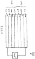
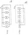
- FIG. 3 is a schematic of a photovoltaic system 300 having a module 310 containing photovoltaic cells 320. Cells 320 are electrically connected in series, and system 300 is electrically connected to a load 330.
- FIG. 4 is a schematic of a photovoltaic system 400 having a module 410 that contains photovoltaic cells 420. Cells 420 are electrically connected in parallel, and system 400 is electrically connected to a load 430.
- some (e.g., all) of the photovoltaic cells in a photovoltaic system can have one or more common substrates.
- some photovoltaic cells in a photovoltaic system are electrically connected in series, and some of the photovoltaic cells in the photovoltaic system are electrically connected in parallel.
- An ITO coated glass substrate was cleaned by sonicating in acetone and isopropanol, respectively. The substrate was then treated with UV/ozone. A thin layer of 3-(2-aminoethyl)aminopropyl trimethoxy silane (AEAP-TMOS) was then blade coated from a solution in 2-methoxyethanol. The film thus formed was allowed to dry on the hot plate. A semiconductor blend of P3HT and C61-PCBM in o-xylene was blade coated onto the film and then dried. A layer of PEDOT (BAYTRON PH with a 0.2 wt% DYNOL surfactant) was blade coated on top of the semiconductor blend.
- PEDOT BAYTRON PH with a 0.2 wt% DYNOL surfactant
- the device was then annealed in a glove box, followed by thermal evaporation of silver as the top metal electrode (100 nm) to form a photovoltaic cell.
- Another photovoltaic cell was prepared in a similar manner except that AEAP-TMOS was not used.
- the results showed that the photovoltaic cell with AEAP-TMOS exhibited much higher injection current under positive voltage than the photovoltaic cell without AEAP-TMOS, indicating that AEAP-TMOS possesses effective electron injection capability.
- the results also showed that the photovoltaic cell with AEAP-TMOS exhibited much lower leakage current under negative voltage than the photovoltaic cell without AEAP-TMOS, indicating that AEAP-TMOS possesses effective hole blocking capability.
- An ITO coated glass substrate was cleaned by sonicating in isopropanol, respectively.
- a thin layer of polyethylenimine and glycerol propoxylate triglycidyl ether (GPTGE) was then blade coated from a solution in isopropanol. The film thus formed was allowed to cure on the hot plate.
- a semiconductor blend of P3HT and C61-PCBM in o-xylene was blade coated onto the film and then dried.
- a hole injecting layer of PEDOT (BAYTRON PH) was blade coated on top of the semiconductor blend. The device was then annealed in a glove box, followed by thermal evaporation of silver as the top metal electrode to form a photovoltaic cell.
- the performance of the photovoltaic cell formed above was measured under AM 1.5 conditions. The results showed that the photovoltaic cell had V oc of 0.57 V, a J sc of 9.05 mA/cm 2 , a fill factor of 0.61, and an efficiency of as high as 3.14%.
Landscapes
- Physics & Mathematics (AREA)
- Electromagnetism (AREA)
- Engineering & Computer Science (AREA)
- Chemical & Material Sciences (AREA)
- Nanotechnology (AREA)
- Mathematical Physics (AREA)
- Theoretical Computer Science (AREA)
- Crystallography & Structural Chemistry (AREA)
- Photovoltaic Devices (AREA)
- Hybrid Cells (AREA)
- Electroluminescent Light Sources (AREA)
Claims (18)
- Article, comprenant :des première et seconde électrodes ;une couche photo-active entre les première et seconde électrodes ; etune seconde couche entre la première électrode et la couche photo-active,dans lequel la seconde couche joue le rôle de couche d'injection d'électrons ou de couche de blocage de trous et elle inclut un composé donneur d'électrons qui est un composé qui contient de l'azote ; dans lequel :l'article est configuré en tant que cellule photovoltaïque ;caractérisé en ce que le composé est un polymère, et le polymère comprend une polyamine.
- Article selon la revendication 1, dans lequel au moins certaines molécules du composé sont adsorbées sur une surface de la première électrode.
- Article selon la revendication 1, dans lequel le polymère est un polyéthylènimine.
- Article selon la revendication 1, dans lequel au moins certaines molécules du polymère sont réticulées au moyen d'un agent de réticulation.
- Article selon la revendication 4, dans lequel l'agent de réticulation comprend un composé qui contient un époxy.
- Article selon la revendication 5, dans lequel l'agent de réticulation comprend du glycérol propoxylate triglycidyl éther ou du glycérol diglycidyl éther.
- Article selon la revendication 1, dans lequel l'article comprend en outre une seconde couche photo-active entre les première et seconde électrodes.
- Article selon la revendication 7, lequel inclut en outre une couche de recombinaison entre les première et seconde couches photo-actives, dans lequel la couche de recombinaison inclut un matériau semiconducteur de type p et un matériau semiconducteur de type n.
- Article selon la revendication 8, dans lequel le matériau semiconducteur de type p et le matériau semiconducteur de type n sont mélangés selon une seule couche.
- Article selon la revendication 8, dans lequel la couche de recombinaison inclut deux couches, une couche qui contient le matériau semiconducteur de type p et l'autre couche qui contient le matériau semiconducteur de type n.
- Article selon la revendication 10, lequel inclut une quatrième couche entre la première couche photo-active et la couche qui contient le matériau semiconducteur de type n, dans lequel la quatrième couche inclut un second composé qui est sélectionné parmi le groupe qui est constitué par les composés qui contiennent de l'azote, les composés qui contiennent du phosphore, les composés qui contiennent du soufre et des combinaisons de ceux-ci.
- Article selon la revendication 8, dans lequel la couche de recombinaison inclut deux couches, une couche qui contient un matériau semiconducteur de type p et l'autre couche qui contient un second composé qui est sélectionné parmi le groupe qui est constitué par les composés qui contiennent de l'azote, les composés qui contiennent du phosphore, les composés qui contiennent du soufre et des combinaisons de ceux-ci.
- Article selon la revendication 12, dans lequel la couche qui contient le second composé est disposée entre la première couche photo-active et la couche qui contient le matériau semiconducteur de type p.
- Article selon la revendication 7, lequel inclut une cellule photovoltaïque en tandem.
- Article selon la revendication 1, dans lequel l'article inclut en outre une couche de transport de trous entre la seconde électrode et la couche photo-active.
- Article selon la revendication 15, dans lequel la couche de transport de trous inclut un polymère qui est sélectionné parmi le groupe qui est constitué par les polythiophènes, les polyanilines, les polyacarbazoles, les polyvinylcarbazoles, les polyphénylènes, les polyvinyl-phénylènes, les polysilanes, les polythiénylènevinylènes, les polyisothianaphtènes et leurs copolymères.
- Article selon la revendication 1, dans lequel l'article inclut en outre une couche de blocage de trous entre la seconde couche et la première électrode.
- Article selon la revendication 17, dans lequel la couche de blocage de trous inclut un matériau qui est sélectionné parmi le groupe qui est constitué par le LiF, les oxydes de métaux et des combinaisons de ceux-ci.
Priority Applications (1)
| Application Number | Priority Date | Filing Date | Title |
|---|---|---|---|
| EP17177395.5A EP3249709A1 (fr) | 2007-04-27 | 2008-04-25 | Cellules photovoltaïques organiques |
Applications Claiming Priority (2)
| Application Number | Priority Date | Filing Date | Title |
|---|---|---|---|
| US92645907P | 2007-04-27 | 2007-04-27 | |
| PCT/US2008/061537 WO2008134492A1 (fr) | 2007-04-27 | 2008-04-25 | Cellules photovoltaïques organiques |
Related Child Applications (2)
| Application Number | Title | Priority Date | Filing Date |
|---|---|---|---|
| EP17177395.5A Division-Into EP3249709A1 (fr) | 2007-04-27 | 2008-04-25 | Cellules photovoltaïques organiques |
| EP17177395.5A Division EP3249709A1 (fr) | 2007-04-27 | 2008-04-25 | Cellules photovoltaïques organiques |
Publications (3)
| Publication Number | Publication Date |
|---|---|
| EP2143144A1 EP2143144A1 (fr) | 2010-01-13 |
| EP2143144A4 EP2143144A4 (fr) | 2016-12-28 |
| EP2143144B1 true EP2143144B1 (fr) | 2018-11-28 |
Family
ID=39885566
Family Applications (2)
| Application Number | Title | Priority Date | Filing Date |
|---|---|---|---|
| EP08746878.1A Not-in-force EP2143144B1 (fr) | 2007-04-27 | 2008-04-25 | Cellules photovoltaiques organiques |
| EP17177395.5A Withdrawn EP3249709A1 (fr) | 2007-04-27 | 2008-04-25 | Cellules photovoltaïques organiques |
Family Applications After (1)
| Application Number | Title | Priority Date | Filing Date |
|---|---|---|---|
| EP17177395.5A Withdrawn EP3249709A1 (fr) | 2007-04-27 | 2008-04-25 | Cellules photovoltaïques organiques |
Country Status (4)
| Country | Link |
|---|---|
| US (1) | US8242356B2 (fr) |
| EP (2) | EP2143144B1 (fr) |
| JP (2) | JP5616783B2 (fr) |
| WO (1) | WO2008134492A1 (fr) |
Cited By (1)
| Publication number | Priority date | Publication date | Assignee | Title |
|---|---|---|---|---|
| US20210402206A1 (en) * | 2018-10-26 | 2021-12-30 | Nippon Shokubai Co., Ltd. | Organic electric field light-emitting sheet for use in light cosmetology or light therapy |
Families Citing this family (63)
| Publication number | Priority date | Publication date | Assignee | Title |
|---|---|---|---|---|
| US20080006324A1 (en) * | 2005-07-14 | 2008-01-10 | Konarka Technologies, Inc. | Tandem Photovoltaic Cells |
| US7781673B2 (en) * | 2005-07-14 | 2010-08-24 | Konarka Technologies, Inc. | Polymers with low band gaps and high charge mobility |
| US20070181179A1 (en) | 2005-12-21 | 2007-08-09 | Konarka Technologies, Inc. | Tandem photovoltaic cells |
| US8158881B2 (en) * | 2005-07-14 | 2012-04-17 | Konarka Technologies, Inc. | Tandem photovoltaic cells |
| US8008421B2 (en) | 2006-10-11 | 2011-08-30 | Konarka Technologies, Inc. | Photovoltaic cell with silole-containing polymer |
| US8008424B2 (en) | 2006-10-11 | 2011-08-30 | Konarka Technologies, Inc. | Photovoltaic cell with thiazole-containing polymer |
| WO2009137141A2 (fr) * | 2008-02-21 | 2009-11-12 | Konarka Technologies, Inc. | Cellules photovoltaïques tandem |
| EP2313926B1 (fr) | 2008-07-16 | 2019-06-12 | Merck Patent GmbH | Procedes de preparation de modules photovoltaiques |
| US8455606B2 (en) | 2008-08-07 | 2013-06-04 | Merck Patent Gmbh | Photoactive polymers |
| JP5580325B2 (ja) * | 2008-11-18 | 2014-08-27 | メルク パテント ゲーエムベーハー | 色素増感光電セル |
| WO2010083161A1 (fr) | 2009-01-13 | 2010-07-22 | Konarka Technologies, Inc. | Module photovoltaïque |
| EP2404333A2 (fr) * | 2009-03-05 | 2012-01-11 | Konarka Technologies, Inc. | Pile solaire ayant plusieurs donneurs d'électrons |
| WO2010107795A1 (fr) | 2009-03-17 | 2010-09-23 | Konarka Technologies, Inc. | Substrat de métal pour une pile photovoltaïque à colorant |
| WO2010107101A1 (fr) * | 2009-03-17 | 2010-09-23 | 住友化学株式会社 | Composition et élément l'utilisant |
| KR101038469B1 (ko) * | 2009-04-13 | 2011-06-01 | 광주과학기술원 | 고분자 전해질층을 이용한 적층형 유기태양전지 및 그 제조방법 |
| RU2538030C2 (ru) | 2009-04-22 | 2015-01-10 | Конинклейке Филипс Электроникс Н.В. | Измерительная система визуализации с печатной матрицей органических фотодиодов |
| WO2010138414A1 (fr) | 2009-05-27 | 2010-12-02 | Konarka Technologies, Inc. | Électrode multicouche réflective |
| JP5648380B2 (ja) * | 2009-09-16 | 2015-01-07 | 三菱化学株式会社 | 光電変換素子及び光電変換素子の製造方法、並びに太陽電池 |
| WO2011085004A2 (fr) | 2010-01-05 | 2011-07-14 | Konarka Technologies, Inc. | Cellule photovoltaïque comprenant un polymère contenant du benzodithiophène |
| JP2013522879A (ja) | 2010-03-09 | 2013-06-13 | コナルカ テクノロジーズ インコーポレイテッド | 緩衝層を備える光起電力モジュール |
| KR101744904B1 (ko) * | 2010-03-22 | 2017-06-21 | 삼성디스플레이 주식회사 | 양자점-블록공중합체 하이브리드 및 이의 제조 방법과 분산 방법, 그리고 양자점 블록공중합체 하이브리드를 포함하는 발광 소자 및 이의 제조 방법 |
| EP2599140A1 (fr) * | 2010-04-06 | 2013-06-05 | Merck Patent GmbH | Electrode innovante |
| JP5633184B2 (ja) * | 2010-05-12 | 2014-12-03 | 三菱化学株式会社 | 光電変換素子 |
| WO2011160021A2 (fr) | 2010-06-17 | 2011-12-22 | Konarka Technologies, Inc. | Dérivés de fullerènes |
| KR101415822B1 (ko) * | 2010-06-29 | 2014-07-09 | 코오롱인더스트리 주식회사 | 유기 태양 전지 및 이의 제조 방법 |
| JP5560132B2 (ja) * | 2010-07-27 | 2014-07-23 | 出光興産株式会社 | 有機薄膜太陽電池用材料及びそれを用いた有機薄膜太陽電池 |
| JP2013542585A (ja) | 2010-09-02 | 2013-11-21 | メルク パテント ゲーエムベーハー | 新規な光活性ポリマーを含む太陽電池 |
| US8778724B2 (en) * | 2010-09-24 | 2014-07-15 | Ut-Battelle, Llc | High volume method of making low-cost, lightweight solar materials |
| JP5644415B2 (ja) * | 2010-11-24 | 2014-12-24 | コニカミノルタ株式会社 | 有機光電変換素子、およびそれを用いた有機太陽電池 |
| EP2684232A4 (fr) * | 2011-03-08 | 2015-05-20 | Univ South Florida | Micro-réseau solaire organique inversé pour applications dans des systèmes micro-électromécaniques |
| US20120234392A1 (en) * | 2011-03-17 | 2012-09-20 | Semiconductor Energy Laboratory Co., Ltd. | Photoelectric conversion device |
| JP6051206B2 (ja) | 2011-04-28 | 2016-12-27 | メルク パテント ゲーエムベーハー | 新規な光活性ポリマー |
| JP2014513443A (ja) * | 2011-05-09 | 2014-05-29 | メルク パテント ゲーエムベーハー | 多接合型光電池 |
| EP2710611B1 (fr) * | 2011-05-16 | 2019-03-20 | Georgia Tech Research Corporation | Procédés de fabrication d'électrodes à faible travail d'extraction et électrode à faible travail d'extraction |
| US9203030B2 (en) * | 2011-05-16 | 2015-12-01 | Georgia Tech Research Corporation | Recyclable organic solar cells on substrates comprising cellulose nanocrystals (CNC) |
| JP5692394B2 (ja) * | 2011-09-08 | 2015-04-01 | 富士通株式会社 | 光電変換素子及びその製造方法 |
| JP5887814B2 (ja) * | 2011-10-07 | 2016-03-16 | 住友化学株式会社 | 高分子化合物及びそれを用いた電子素子 |
| WO2013065573A1 (fr) * | 2011-10-31 | 2013-05-10 | コニカミノルタ株式会社 | Convertisseur photoélectrique organique et photopile utilisant ledit convertisseur |
| KR20150003181A (ko) * | 2012-03-14 | 2015-01-08 | 더 트러스티즈 오브 프린스턴 유니버시티 | 실리콘 태양광발전을 위한 정공 차단 실리콘/티탄 산화물 헤테로접합 |
| US20130263925A1 (en) | 2012-04-05 | 2013-10-10 | Merck Patent Gmbh | Hole Carrier Layer For Organic Photovoltaic Device |
| DE112012006595T5 (de) * | 2012-06-29 | 2015-04-02 | Sanyo Electric Co., Ltd. | Solarzelle |
| JP6083539B2 (ja) * | 2012-06-29 | 2017-02-22 | パナソニックIpマネジメント株式会社 | 太陽電池 |
| JP2014027174A (ja) * | 2012-07-27 | 2014-02-06 | Mitsubishi Chemicals Corp | 光電変換素子、太陽電池モジュール、及び光電変換素子の製造方法 |
| JP5983190B2 (ja) * | 2012-08-29 | 2016-08-31 | 三菱化学株式会社 | 有機薄膜太陽電池素子の製造方法 |
| CN103311439B (zh) * | 2013-05-17 | 2015-07-15 | 中国科学院化学研究所 | 薄膜光电导探测器及其制备方法与应用 |
| JP2015012114A (ja) * | 2013-06-28 | 2015-01-19 | 信越化学工業株式会社 | 太陽電池モジュール及びその製造方法 |
| US9293632B2 (en) * | 2013-09-18 | 2016-03-22 | Globalfoundries Inc. | Pressure transfer process for thin film solar cell fabrication |
| US20160329510A1 (en) * | 2013-12-26 | 2016-11-10 | Merck Patent Gmbh | Photovoltaic cells |
| JP6114710B2 (ja) * | 2014-03-27 | 2017-04-12 | 富士フイルム株式会社 | 太陽電池 |
| WO2015159755A1 (fr) * | 2014-04-14 | 2015-10-22 | 東レ株式会社 | Élément photovoltaïque |
| JP6641692B2 (ja) * | 2015-01-05 | 2020-02-05 | 株式会社リコー | 光電変換素子 |
| JP6743812B2 (ja) * | 2015-05-12 | 2020-08-19 | 住友化学株式会社 | 有機光電変換素子 |
| JP6657841B2 (ja) * | 2015-11-20 | 2020-03-04 | 株式会社リコー | 光電変換素子及び太陽電池 |
| US10686134B2 (en) * | 2016-01-28 | 2020-06-16 | Ricoh Company, Ltd. | Photoelectric conversion element |
| JP6690276B2 (ja) * | 2016-02-09 | 2020-04-28 | 株式会社リコー | 光電変換素子 |
| JP6671599B2 (ja) * | 2016-05-20 | 2020-03-25 | 株式会社リコー | 有機材料および光電変換素子 |
| EP3484528B1 (fr) | 2016-07-18 | 2020-11-25 | Janssen Pharmaceutica NV | Ligands d'imagerie tep pour la protéine tau |
| AT519193A1 (de) * | 2016-09-01 | 2018-04-15 | Univ Linz | Optoelektronischer Infrarotsensor |
| US11183637B2 (en) | 2016-10-05 | 2021-11-23 | Raynergy Tek Incorporation | Organic photodetector |
| EP3375017B1 (fr) | 2016-10-24 | 2021-08-11 | Indian Institute of Technology, Guwahati | Dispositif de collecte d'énergie électrique microfluidique |
| JP7112708B2 (ja) * | 2018-02-14 | 2022-08-04 | 国立大学法人山形大学 | 有機el素子 |
| CN112390947B (zh) * | 2019-08-16 | 2023-04-28 | 位速科技股份有限公司 | 电极界面层材料、两性离子聚合物和有机光伏元件 |
| KR102505709B1 (ko) * | 2021-02-05 | 2023-03-03 | 광주과학기술원 | 역구조 유기태양전지 및 이의 제조 방법 |
Citations (1)
| Publication number | Priority date | Publication date | Assignee | Title |
|---|---|---|---|---|
| EP1319989A2 (fr) * | 2001-12-14 | 2003-06-18 | Xerox Corporation | Elément de formation d'images électrophotographiques |
Family Cites Families (36)
| Publication number | Priority date | Publication date | Assignee | Title |
|---|---|---|---|---|
| US5155200A (en) * | 1990-04-20 | 1992-10-13 | Xerox Corporation | Polyarylamine polymers |
| EP0549345B1 (fr) * | 1991-12-24 | 1997-03-05 | MITSUI TOATSU CHEMICALS, Inc. | Elément électroluminescent à couche mince organique |
| JPH11335651A (ja) * | 1998-05-28 | 1999-12-07 | Nippon Nsc Ltd | 水系接着剤組成物 |
| US6451415B1 (en) * | 1998-08-19 | 2002-09-17 | The Trustees Of Princeton University | Organic photosensitive optoelectronic device with an exciton blocking layer |
| US6198092B1 (en) * | 1998-08-19 | 2001-03-06 | The Trustees Of Princeton University | Stacked organic photosensitive optoelectronic devices with an electrically parallel configuration |
| NO312867B1 (no) * | 1999-06-30 | 2002-07-08 | Penn State Res Found | Anordning til elektrisk kontaktering eller isolering av organiske eller uorganiske halvledere, samt fremgangsmåte til densfremstilling |
| US9607301B2 (en) * | 2000-04-27 | 2017-03-28 | Merck Patent Gmbh | Photovoltaic sensor facilities in a home environment |
| US7022910B2 (en) | 2002-03-29 | 2006-04-04 | Konarka Technologies, Inc. | Photovoltaic cells utilizing mesh electrodes |
| WO2002101838A1 (fr) * | 2001-06-11 | 2002-12-19 | The Trustees Of Princeton University | Dispositifs organiques photovoltaiques |
| US6596450B2 (en) * | 2001-09-10 | 2003-07-22 | Xerox Corporation | Charge transport components |
| US6866949B2 (en) * | 2002-03-08 | 2005-03-15 | Dai Nippon Printing Co., Ltd. | Substrate film, gas barrier film, and display using the same |
| JP2004250522A (ja) * | 2003-02-19 | 2004-09-09 | Kawamura Inst Of Chem Res | 重合体、重合体の製造方法、有機エレクトロルミネッセンス素子、および有機エレクトロルミネッセンス素子用正孔輸送層の製造方法 |
| KR101036539B1 (ko) | 2003-03-24 | 2011-05-24 | 코나르카 테크놀로지, 인코포레이티드 | 메쉬 전극을 갖는 광전지 |
| US6858363B2 (en) * | 2003-04-04 | 2005-02-22 | Xerox Corporation | Photoconductive imaging members |
| JP4596409B2 (ja) * | 2003-04-21 | 2010-12-08 | 株式会社東京技術研究所 | バルブ装着用ヒータユニット |
| TWI373483B (en) * | 2003-04-22 | 2012-10-01 | Du Pont | Water dispersible polythiophenes made with polymeric acid colloids |
| GB0309355D0 (en) | 2003-04-24 | 2003-06-04 | Univ Cambridge Tech | Organic electronic devices incorporating semiconducting polymer |
| DE10326547A1 (de) * | 2003-06-12 | 2005-01-05 | Siemens Ag | Tandemsolarzelle mit einer gemeinsamen organischen Elektrode |
| JP4824913B2 (ja) * | 2004-02-17 | 2011-11-30 | 国立大学法人京都大学 | グラフト薄膜を用いた光電素子及び太陽電池 |
| JP2005236794A (ja) * | 2004-02-20 | 2005-09-02 | Fuji Photo Film Co Ltd | デジタルカメラ |
| DE102004008304A1 (de) * | 2004-02-20 | 2005-09-08 | Covion Organic Semiconductors Gmbh | Organische elektronische Vorrichtungen |
| DE102004021567A1 (de) * | 2004-05-03 | 2005-12-08 | Covion Organic Semiconductors Gmbh | Elektronische Vorrichtungen enthaltend organische Halbleiter |
| US7772484B2 (en) | 2004-06-01 | 2010-08-10 | Konarka Technologies, Inc. | Photovoltaic module architecture |
| US20050288182A1 (en) * | 2004-06-18 | 2005-12-29 | Kazushi Torii | Water absorbent resin composition and production method thereof |
| JP2006073583A (ja) * | 2004-08-31 | 2006-03-16 | Toray Ind Inc | 光電変換素子用材料およびこれを用いた光電変換素子 |
| US20060112983A1 (en) * | 2004-11-17 | 2006-06-01 | Nanosys, Inc. | Photoactive devices and components with enhanced efficiency |
| BRPI0516786A (pt) * | 2004-11-24 | 2008-09-23 | Univ Princeton | dispositivo optoeletrÈnico fotosensìvel orgánico tendo uma camada bloqueadora de éxcitons de fenantrolina |
| US7985490B2 (en) * | 2005-02-14 | 2011-07-26 | Samsung Mobile Display Co., Ltd. | Composition of conducting polymer and organic opto-electronic device employing the same |
| US7825326B2 (en) * | 2005-03-21 | 2010-11-02 | Konarka Technologies, Inc. | Polymer photovoltaic cell |
| US20060225778A1 (en) * | 2005-03-21 | 2006-10-12 | Christoph Brabec | Photovoltaic module |
| KR101213484B1 (ko) * | 2005-05-19 | 2012-12-20 | 삼성디스플레이 주식회사 | 전도성 고분자 조성물 및 이를 채용한 유기 광전 소자 |
| US7541123B2 (en) * | 2005-06-20 | 2009-06-02 | Xerox Corporation | Imaging member |
| JP5096336B2 (ja) * | 2005-09-01 | 2012-12-12 | コナルカ テクノロジーズ インコーポレイテッド | バイパスダイオードと一体化した光電池を備えるシステム |
| JP4677314B2 (ja) * | 2005-09-20 | 2011-04-27 | 富士フイルム株式会社 | センサーおよび有機光電変換素子の駆動方法 |
| GB2430679A (en) * | 2005-09-28 | 2007-04-04 | Riso Nat Lab | Photovoltaic polymer |
| JP5118296B2 (ja) * | 2005-10-19 | 2013-01-16 | パナソニック株式会社 | 積層型有機太陽電池 |
-
2008
- 2008-04-25 EP EP08746878.1A patent/EP2143144B1/fr not_active Not-in-force
- 2008-04-25 WO PCT/US2008/061537 patent/WO2008134492A1/fr not_active Ceased
- 2008-04-25 EP EP17177395.5A patent/EP3249709A1/fr not_active Withdrawn
- 2008-04-25 US US12/109,828 patent/US8242356B2/en not_active Expired - Fee Related
- 2008-04-25 JP JP2010506512A patent/JP5616783B2/ja not_active Expired - Fee Related
-
2013
- 2013-07-31 JP JP2013159592A patent/JP5613303B2/ja not_active Expired - Fee Related
Patent Citations (1)
| Publication number | Priority date | Publication date | Assignee | Title |
|---|---|---|---|---|
| EP1319989A2 (fr) * | 2001-12-14 | 2003-06-18 | Xerox Corporation | Elément de formation d'images électrophotographiques |
Cited By (1)
| Publication number | Priority date | Publication date | Assignee | Title |
|---|---|---|---|---|
| US20210402206A1 (en) * | 2018-10-26 | 2021-12-30 | Nippon Shokubai Co., Ltd. | Organic electric field light-emitting sheet for use in light cosmetology or light therapy |
Also Published As
| Publication number | Publication date |
|---|---|
| EP2143144A1 (fr) | 2010-01-13 |
| JP5616783B2 (ja) | 2014-10-29 |
| JP5613303B2 (ja) | 2014-10-22 |
| US20080264488A1 (en) | 2008-10-30 |
| US8242356B2 (en) | 2012-08-14 |
| EP3249709A1 (fr) | 2017-11-29 |
| EP2143144A4 (fr) | 2016-12-28 |
| WO2008134492A1 (fr) | 2008-11-06 |
| JP2013236103A (ja) | 2013-11-21 |
| JP2010525613A (ja) | 2010-07-22 |
Similar Documents
| Publication | Publication Date | Title |
|---|---|---|
| US8242356B2 (en) | Organic photovoltaic cells | |
| EP2139616B1 (fr) | Nouvelle electrode | |
| US8178779B2 (en) | Organic photovoltaic cells | |
| EP2321861B1 (fr) | Nouveaux copolymères photo-actifs | |
| US20070289626A1 (en) | Photovoltaic cells | |
| US20100224252A1 (en) | Photovoltaic Cell Having Multiple Electron Donors | |
| US20070193621A1 (en) | Photovoltaic cells | |
| EP2707907B1 (fr) | Cellules photovoltaïques en tandem | |
| WO2009070534A1 (fr) | Cellules photovoltaïques organiques | |
| KR101033304B1 (ko) | 발광특성을 가지는 유기 태양전지 및 그 제조방법 | |
| KR20180004470A (ko) | 페로브스카이트 구조의 화합물, 이를 이용한 태양전지 및 박막트랜지스터 | |
| WO2007104039A2 (fr) | Cellules photovoltaïques | |
| KR20220170311A (ko) | 후열처리를 이용한 광소자 제조 방법 | |
| KR102690507B1 (ko) | 페로브스카이트 태양전지 및 이의 제조방법 | |
| WO2010138414A1 (fr) | Électrode multicouche réflective |
Legal Events
| Date | Code | Title | Description |
|---|---|---|---|
| PUAI | Public reference made under article 153(3) epc to a published international application that has entered the european phase |
Free format text: ORIGINAL CODE: 0009012 |
|
| 17P | Request for examination filed |
Effective date: 20091105 |
|
| AK | Designated contracting states |
Kind code of ref document: A1 Designated state(s): AT BE BG CH CY CZ DE DK EE ES FI FR GB GR HR HU IE IS IT LI LT LU LV MC MT NL NO PL PT RO SE SI SK TR |
|
| RIN1 | Information on inventor provided before grant (corrected) |
Inventor name: LEE, MICHAEL Inventor name: DENNLER, GILLES Inventor name: COAKLEY, KEVIN Inventor name: BALASUBRAMANIAN, SRINI |
|
| DAX | Request for extension of the european patent (deleted) | ||
| RIN1 | Information on inventor provided before grant (corrected) |
Inventor name: LEE, MICHAEL Inventor name: BALASUBRAMANIAN, SRINI Inventor name: DENNLER, GILLES Inventor name: GAUDIANA, RUSSELL Inventor name: COAKLEY, KEVIN |
|
| 19U | Interruption of proceedings before grant |
Effective date: 20120601 |
|
| 19W | Proceedings resumed before grant after interruption of proceedings |
Effective date: 20130301 |
|
| RAP1 | Party data changed (applicant data changed or rights of an application transferred) |
Owner name: MERCK PATENT GMBH |
|
| RIC1 | Information provided on ipc code assigned before grant |
Ipc: H01L 51/46 20060101ALI20160817BHEP Ipc: H01L 27/30 20060101ALI20160817BHEP Ipc: H01L 51/44 20060101AFI20160817BHEP |
|
| REG | Reference to a national code |
Ref country code: DE Ref legal event code: R079 Ref document number: 602008058098 Country of ref document: DE Free format text: PREVIOUS MAIN CLASS: H01L0031000000 Ipc: H01L0051440000 |
|
| RA4 | Supplementary search report drawn up and despatched (corrected) |
Effective date: 20161128 |
|
| RIC1 | Information provided on ipc code assigned before grant |
Ipc: H01L 51/44 20060101AFI20161122BHEP Ipc: H01L 51/46 20060101ALI20161122BHEP Ipc: H01L 27/30 20060101ALI20161122BHEP |
|
| STAA | Information on the status of an ep patent application or granted ep patent |
Free format text: STATUS: EXAMINATION IS IN PROGRESS |
|
| 17Q | First examination report despatched |
Effective date: 20180228 |
|
| GRAP | Despatch of communication of intention to grant a patent |
Free format text: ORIGINAL CODE: EPIDOSNIGR1 |
|
| STAA | Information on the status of an ep patent application or granted ep patent |
Free format text: STATUS: GRANT OF PATENT IS INTENDED |
|
| INTG | Intention to grant announced |
Effective date: 20180719 |
|
| GRAS | Grant fee paid |
Free format text: ORIGINAL CODE: EPIDOSNIGR3 |
|
| GRAA | (expected) grant |
Free format text: ORIGINAL CODE: 0009210 |
|
| STAA | Information on the status of an ep patent application or granted ep patent |
Free format text: STATUS: THE PATENT HAS BEEN GRANTED |
|
| AK | Designated contracting states |
Kind code of ref document: B1 Designated state(s): AT BE BG CH CY CZ DE DK EE ES FI FR GB GR HR HU IE IS IT LI LT LU LV MC MT NL NO PL PT RO SE SI SK TR |
|
| REG | Reference to a national code |
Ref country code: GB Ref legal event code: FG4D |
|
| REG | Reference to a national code |
Ref country code: CH Ref legal event code: EP |
|
| REG | Reference to a national code |
Ref country code: AT Ref legal event code: REF Ref document number: 1071258 Country of ref document: AT Kind code of ref document: T Effective date: 20181215 |
|
| REG | Reference to a national code |
Ref country code: DE Ref legal event code: R096 Ref document number: 602008058098 Country of ref document: DE |
|
| REG | Reference to a national code |
Ref country code: IE Ref legal event code: FG4D |
|
| REG | Reference to a national code |
Ref country code: NL Ref legal event code: MP Effective date: 20181128 |
|
| REG | Reference to a national code |
Ref country code: LT Ref legal event code: MG4D |
|
| REG | Reference to a national code |
Ref country code: AT Ref legal event code: MK05 Ref document number: 1071258 Country of ref document: AT Kind code of ref document: T Effective date: 20181128 |
|
| PG25 | Lapsed in a contracting state [announced via postgrant information from national office to epo] |
Ref country code: ES Free format text: LAPSE BECAUSE OF FAILURE TO SUBMIT A TRANSLATION OF THE DESCRIPTION OR TO PAY THE FEE WITHIN THE PRESCRIBED TIME-LIMIT Effective date: 20181128 Ref country code: LV Free format text: LAPSE BECAUSE OF FAILURE TO SUBMIT A TRANSLATION OF THE DESCRIPTION OR TO PAY THE FEE WITHIN THE PRESCRIBED TIME-LIMIT Effective date: 20181128 Ref country code: HR Free format text: LAPSE BECAUSE OF FAILURE TO SUBMIT A TRANSLATION OF THE DESCRIPTION OR TO PAY THE FEE WITHIN THE PRESCRIBED TIME-LIMIT Effective date: 20181128 Ref country code: BG Free format text: LAPSE BECAUSE OF FAILURE TO SUBMIT A TRANSLATION OF THE DESCRIPTION OR TO PAY THE FEE WITHIN THE PRESCRIBED TIME-LIMIT Effective date: 20190228 Ref country code: LT Free format text: LAPSE BECAUSE OF FAILURE TO SUBMIT A TRANSLATION OF THE DESCRIPTION OR TO PAY THE FEE WITHIN THE PRESCRIBED TIME-LIMIT Effective date: 20181128 Ref country code: IS Free format text: LAPSE BECAUSE OF FAILURE TO SUBMIT A TRANSLATION OF THE DESCRIPTION OR TO PAY THE FEE WITHIN THE PRESCRIBED TIME-LIMIT Effective date: 20190328 Ref country code: FI Free format text: LAPSE BECAUSE OF FAILURE TO SUBMIT A TRANSLATION OF THE DESCRIPTION OR TO PAY THE FEE WITHIN THE PRESCRIBED TIME-LIMIT Effective date: 20181128 Ref country code: NO Free format text: LAPSE BECAUSE OF FAILURE TO SUBMIT A TRANSLATION OF THE DESCRIPTION OR TO PAY THE FEE WITHIN THE PRESCRIBED TIME-LIMIT Effective date: 20190228 Ref country code: AT Free format text: LAPSE BECAUSE OF FAILURE TO SUBMIT A TRANSLATION OF THE DESCRIPTION OR TO PAY THE FEE WITHIN THE PRESCRIBED TIME-LIMIT Effective date: 20181128 |
|
| PG25 | Lapsed in a contracting state [announced via postgrant information from national office to epo] |
Ref country code: SE Free format text: LAPSE BECAUSE OF FAILURE TO SUBMIT A TRANSLATION OF THE DESCRIPTION OR TO PAY THE FEE WITHIN THE PRESCRIBED TIME-LIMIT Effective date: 20181128 Ref country code: GR Free format text: LAPSE BECAUSE OF FAILURE TO SUBMIT A TRANSLATION OF THE DESCRIPTION OR TO PAY THE FEE WITHIN THE PRESCRIBED TIME-LIMIT Effective date: 20190301 Ref country code: PT Free format text: LAPSE BECAUSE OF FAILURE TO SUBMIT A TRANSLATION OF THE DESCRIPTION OR TO PAY THE FEE WITHIN THE PRESCRIBED TIME-LIMIT Effective date: 20190328 |
|
| PG25 | Lapsed in a contracting state [announced via postgrant information from national office to epo] |
Ref country code: NL Free format text: LAPSE BECAUSE OF FAILURE TO SUBMIT A TRANSLATION OF THE DESCRIPTION OR TO PAY THE FEE WITHIN THE PRESCRIBED TIME-LIMIT Effective date: 20181128 |
|
| PG25 | Lapsed in a contracting state [announced via postgrant information from national office to epo] |
Ref country code: IT Free format text: LAPSE BECAUSE OF FAILURE TO SUBMIT A TRANSLATION OF THE DESCRIPTION OR TO PAY THE FEE WITHIN THE PRESCRIBED TIME-LIMIT Effective date: 20181128 Ref country code: DK Free format text: LAPSE BECAUSE OF FAILURE TO SUBMIT A TRANSLATION OF THE DESCRIPTION OR TO PAY THE FEE WITHIN THE PRESCRIBED TIME-LIMIT Effective date: 20181128 Ref country code: PL Free format text: LAPSE BECAUSE OF FAILURE TO SUBMIT A TRANSLATION OF THE DESCRIPTION OR TO PAY THE FEE WITHIN THE PRESCRIBED TIME-LIMIT Effective date: 20181128 Ref country code: CZ Free format text: LAPSE BECAUSE OF FAILURE TO SUBMIT A TRANSLATION OF THE DESCRIPTION OR TO PAY THE FEE WITHIN THE PRESCRIBED TIME-LIMIT Effective date: 20181128 |
|
| REG | Reference to a national code |
Ref country code: DE Ref legal event code: R097 Ref document number: 602008058098 Country of ref document: DE |
|
| PG25 | Lapsed in a contracting state [announced via postgrant information from national office to epo] |
Ref country code: RO Free format text: LAPSE BECAUSE OF FAILURE TO SUBMIT A TRANSLATION OF THE DESCRIPTION OR TO PAY THE FEE WITHIN THE PRESCRIBED TIME-LIMIT Effective date: 20181128 Ref country code: SK Free format text: LAPSE BECAUSE OF FAILURE TO SUBMIT A TRANSLATION OF THE DESCRIPTION OR TO PAY THE FEE WITHIN THE PRESCRIBED TIME-LIMIT Effective date: 20181128 Ref country code: EE Free format text: LAPSE BECAUSE OF FAILURE TO SUBMIT A TRANSLATION OF THE DESCRIPTION OR TO PAY THE FEE WITHIN THE PRESCRIBED TIME-LIMIT Effective date: 20181128 |
|
| PLBE | No opposition filed within time limit |
Free format text: ORIGINAL CODE: 0009261 |
|
| STAA | Information on the status of an ep patent application or granted ep patent |
Free format text: STATUS: NO OPPOSITION FILED WITHIN TIME LIMIT |
|
| PG25 | Lapsed in a contracting state [announced via postgrant information from national office to epo] |
Ref country code: SI Free format text: LAPSE BECAUSE OF FAILURE TO SUBMIT A TRANSLATION OF THE DESCRIPTION OR TO PAY THE FEE WITHIN THE PRESCRIBED TIME-LIMIT Effective date: 20181128 |
|
| 26N | No opposition filed |
Effective date: 20190829 |
|
| REG | Reference to a national code |
Ref country code: CH Ref legal event code: PL |
|
| REG | Reference to a national code |
Ref country code: BE Ref legal event code: MM Effective date: 20190430 |
|
| PG25 | Lapsed in a contracting state [announced via postgrant information from national office to epo] |
Ref country code: LU Free format text: LAPSE BECAUSE OF NON-PAYMENT OF DUE FEES Effective date: 20190425 Ref country code: MC Free format text: LAPSE BECAUSE OF FAILURE TO SUBMIT A TRANSLATION OF THE DESCRIPTION OR TO PAY THE FEE WITHIN THE PRESCRIBED TIME-LIMIT Effective date: 20181128 |
|
| PG25 | Lapsed in a contracting state [announced via postgrant information from national office to epo] |
Ref country code: CH Free format text: LAPSE BECAUSE OF NON-PAYMENT OF DUE FEES Effective date: 20190430 Ref country code: LI Free format text: LAPSE BECAUSE OF NON-PAYMENT OF DUE FEES Effective date: 20190430 |
|
| PG25 | Lapsed in a contracting state [announced via postgrant information from national office to epo] |
Ref country code: BE Free format text: LAPSE BECAUSE OF NON-PAYMENT OF DUE FEES Effective date: 20190430 |
|
| PG25 | Lapsed in a contracting state [announced via postgrant information from national office to epo] |
Ref country code: TR Free format text: LAPSE BECAUSE OF FAILURE TO SUBMIT A TRANSLATION OF THE DESCRIPTION OR TO PAY THE FEE WITHIN THE PRESCRIBED TIME-LIMIT Effective date: 20181128 |
|
| PG25 | Lapsed in a contracting state [announced via postgrant information from national office to epo] |
Ref country code: IE Free format text: LAPSE BECAUSE OF NON-PAYMENT OF DUE FEES Effective date: 20190425 |
|
| PG25 | Lapsed in a contracting state [announced via postgrant information from national office to epo] |
Ref country code: CY Free format text: LAPSE BECAUSE OF FAILURE TO SUBMIT A TRANSLATION OF THE DESCRIPTION OR TO PAY THE FEE WITHIN THE PRESCRIBED TIME-LIMIT Effective date: 20181128 |
|
| PG25 | Lapsed in a contracting state [announced via postgrant information from national office to epo] |
Ref country code: HU Free format text: LAPSE BECAUSE OF FAILURE TO SUBMIT A TRANSLATION OF THE DESCRIPTION OR TO PAY THE FEE WITHIN THE PRESCRIBED TIME-LIMIT; INVALID AB INITIO Effective date: 20080425 Ref country code: MT Free format text: LAPSE BECAUSE OF FAILURE TO SUBMIT A TRANSLATION OF THE DESCRIPTION OR TO PAY THE FEE WITHIN THE PRESCRIBED TIME-LIMIT Effective date: 20181128 |
|
| PGFP | Annual fee paid to national office [announced via postgrant information from national office to epo] |
Ref country code: GB Payment date: 20220421 Year of fee payment: 15 |
|
| REG | Reference to a national code |
Ref country code: DE Ref legal event code: R079 Ref document number: 602008058098 Country of ref document: DE Free format text: PREVIOUS MAIN CLASS: H01L0051440000 Ipc: H10K0030800000 |
|
| REG | Reference to a national code |
Ref country code: DE Ref legal event code: R081 Ref document number: 602008058098 Country of ref document: DE Owner name: ASCA, FR Free format text: FORMER OWNER: MERCK PATENT GMBH, 64293 DARMSTADT, DE Ref country code: DE Ref legal event code: R081 Ref document number: 602008058098 Country of ref document: DE Owner name: ASCA GMBH & CO. KG, DE Free format text: FORMER OWNER: MERCK PATENT GMBH, 64293 DARMSTADT, DE |
|
| P01 | Opt-out of the competence of the unified patent court (upc) registered |
Effective date: 20230525 |
|
| GBPC | Gb: european patent ceased through non-payment of renewal fee |
Effective date: 20230425 |
|
| REG | Reference to a national code |
Ref country code: DE Ref legal event code: R082 Ref document number: 602008058098 Country of ref document: DE Representative=s name: FDST PATENTANWAELTE FREIER DOERR STAMMLER TSCH, DE Ref country code: DE Ref legal event code: R081 Ref document number: 602008058098 Country of ref document: DE Owner name: ASCA GMBH & CO. KG, DE Free format text: FORMER OWNER: ASCA, NANTES, FR |
|
| PG25 | Lapsed in a contracting state [announced via postgrant information from national office to epo] |
Ref country code: GB Free format text: LAPSE BECAUSE OF NON-PAYMENT OF DUE FEES Effective date: 20230425 |
|
| PG25 | Lapsed in a contracting state [announced via postgrant information from national office to epo] |
Ref country code: GB Free format text: LAPSE BECAUSE OF NON-PAYMENT OF DUE FEES Effective date: 20230425 |
|
| PGFP | Annual fee paid to national office [announced via postgrant information from national office to epo] |
Ref country code: DE Payment date: 20240425 Year of fee payment: 17 |
|
| PGFP | Annual fee paid to national office [announced via postgrant information from national office to epo] |
Ref country code: FR Payment date: 20240419 Year of fee payment: 17 |
|
| REG | Reference to a national code |
Ref country code: DE Ref legal event code: R119 Ref document number: 602008058098 Country of ref document: DE |
|
| PG25 | Lapsed in a contracting state [announced via postgrant information from national office to epo] |
Ref country code: DE Free format text: LAPSE BECAUSE OF NON-PAYMENT OF DUE FEES Effective date: 20251104 |
|
| PG25 | Lapsed in a contracting state [announced via postgrant information from national office to epo] |
Ref country code: FR Free format text: LAPSE BECAUSE OF NON-PAYMENT OF DUE FEES Effective date: 20250430 |