EP2143184B1 - Verfahren zum selektiven auslösen von leistungsschaltern - Google Patents
Verfahren zum selektiven auslösen von leistungsschaltern Download PDFInfo
- Publication number
- EP2143184B1 EP2143184B1 EP08736632.4A EP08736632A EP2143184B1 EP 2143184 B1 EP2143184 B1 EP 2143184B1 EP 08736632 A EP08736632 A EP 08736632A EP 2143184 B1 EP2143184 B1 EP 2143184B1
- Authority
- EP
- European Patent Office
- Prior art keywords
- circuit
- breaker
- upstream
- short
- downstream
- Prior art date
- Legal status (The legal status is an assumption and is not a legal conclusion. Google has not performed a legal analysis and makes no representation as to the accuracy of the status listed.)
- Not-in-force
Links
- 238000000034 method Methods 0.000 title claims description 14
- 238000011144 upstream manufacturing Methods 0.000 claims description 24
- 230000001419 dependent effect Effects 0.000 claims description 6
- 230000004913 activation Effects 0.000 claims description 4
- 230000015572 biosynthetic process Effects 0.000 claims 1
- 240000006829 Ficus sundaica Species 0.000 description 1
- 206010000210 abortion Diseases 0.000 description 1
- 230000006978 adaptation Effects 0.000 description 1
- 230000002950 deficient Effects 0.000 description 1
- 238000001514 detection method Methods 0.000 description 1
- 238000012544 monitoring process Methods 0.000 description 1
Images

Classifications
-
- H—ELECTRICITY
- H02—GENERATION; CONVERSION OR DISTRIBUTION OF ELECTRIC POWER
- H02H—EMERGENCY PROTECTIVE CIRCUIT ARRANGEMENTS
- H02H7/00—Emergency protective circuit arrangements specially adapted for specific types of electric machines or apparatus or for sectionalised protection of cable or line systems, and effecting automatic switching in the event of an undesired change from normal working conditions
- H02H7/26—Sectionalised protection of cable or line systems, e.g. for disconnecting a section on which a short-circuit, earth fault, or arc discharge has occured
- H02H7/30—Staggered disconnection
-
- H—ELECTRICITY
- H02—GENERATION; CONVERSION OR DISTRIBUTION OF ELECTRIC POWER
- H02H—EMERGENCY PROTECTIVE CIRCUIT ARRANGEMENTS
- H02H1/00—Details of emergency protective circuit arrangements
- H02H1/0007—Details of emergency protective circuit arrangements concerning the detecting means
- H02H1/0015—Using arc detectors
Definitions
- the invention relates to a method for the selective release of an upstream and at least one subordinate circuit breaker according to the preamble of claim 1.
- circuit breakers in the event of a short circuit. This means that in each case the circuit breaker triggers, which is closest to the short circuit seen from the power supply, so that no more consumers are unavoidably affected by the shutdown.
- the mutually before and downstream circuit breakers are subject to a current and time graduation; In each case, the circuit breakers close to the supply point have longer switch-off times than the downstream ones. This ensures that the upstream circuit breakers only switch off when they are closest to the short circuit or in emergencies where a downstream circuit breaker does not trip although it should trip.
- the current-time characteristics of the circuit breakers are coordinated so that they trigger in the event of a short circuit in the feed direction at ever higher currents and for ever longer periods.
- WO 2006/108860 A1 is a method and an arrangement for increasing and ensuring the selectivity of a switching device in a group of switching devices and a use of the arrangement when switching in circuits known.
- a method for increasing and ensuring the selectivity of a switching device in a group of switching devices wherein the switching device group at least two circuits are associated with a first, upstream switch and at least a second, downstream switch, the following measures are performed: it is the impedance of the circuit Determining and analyzing, for impedance determination, the elements of the circuit present in the circuit of the upstream switch, such as bus bars, lines or the like, are taken into account and the impedance analysis improves the selectivity.
- a microprocessor is used for selectivity, wherein the microprocessor arranged in the upstream switch is.
- the object of the invention is to provide a simplified method for selective release, which is particularly applicable to the very short turn-off of the low-voltage circuit breakers.
- the solution provides that the switching arc is present for the upstream circuit breaker when the output side ohmic resistance of the short-circuit loop formed by the upstream circuit breaker has an exponential time course.
- the upstream circuit breaker can determine each case of itself, whether a downstream circuit breaker generates a switching arc and thus whether it already shuts off. In this case, it no longer comes to a then unwanted shutdown by the upstream circuit breaker.
- no additional circuit complexity and no communication between the circuit breakers with each other is required for this solution.
- the upstream circuit breaker has a back-up function and he this back-up function and the output side impedance monitors that only after activation of the back-up function and / or if the output-side impedance is within a predetermined impedance range, the downstream occurrence of a switching arc is monitored for a predetermined time and triggers the upstream circuit breaker, if in the predetermined time no switching arc occurs.
- a better adaptation of the method is achieved if the predetermined time, from the short circuit onset to the detection of a downstream switching arc, is current-dependent.
- FIG. 1 shows a schematic representation of a circuit arrangement with multiple circuit breakers in the form of circuit breakers LS, of which in the FIG. 1 only three circuit breakers LS1, LS2, LSn are shown.
- the circuit breakers LS are current-limiting low-voltage circuit breakers, which have very short and dependent on the amount of short-circuit current stop times.
- the Interrupt U serves to simplify the representation of the circuit arrangement; it says that between the circuit breakers LS2 and LSn shown, even more circuit breakers LS can be present.
- a power supply 1 is shown, to which a power grid 2 and a transformer 3 belong.
- the power supply 1 follows the (near-feed) circuit breaker LS1, which is upstream of the circuit breakers LS2, LSn. Accordingly, the two power switches LS2, LSn downstream of the power switch LS1. "Upstream” and “downstream” are defined as viewed from the power supply 1, respectively.
- FIG. 1 further shows that the circuit breaker LS2 closest to the fault location F2.5 is already in the process of opening and thus disconnecting the short-circuit loop formed by the short-circuit 4 from the power supply 1.
- the opening switching contacts of the circuit breaker LS2 pull in FIG. 1 shown switching arc 5, which is deleted in a further opening of the switch contacts and consequently extinguished again when completely open switch contacts.
- the circuit breaker LS1 has a back-up function, i. it also opens slightly (together with the circuit-breaker LS2), when the short-circuit 4 is seen from the power supply 1 before its threshold 6 and the short-circuit current has exceeded a minimum value. Due to the back-up function of the circuit breaker LS1, the flowing current I is already limited.
- the short circuit 4 is not present but behind the threshold 6, so that the back-up function of the circuit breaker LS1 is not active.
- the short-circuit 4 and the threshold 6 within a range 6a, which schematically indicates the protection or effective range of the power supply circuit breaker LS1, ie in which the output-side impedance R (s. FIG. 2 ) significantly changes when a short circuit 4 occurs.
- the upstream power switch LS1 monitors (monitors) its back-up function (eg by means of photodiodes or motion sensors) and the output-side impedance, ie the impedance present from the power switch LS1 in the direction of the power switches LS2, LSn. It has an ohmic component (ohmic resistance R in FIG. 2 ) as well as an imaginary part. Due to the short-circuit 4, the output-side impedance is reduced, since a short-circuiting loop is produced by the short-circuit 4 within the circuit arrangement. The circuit breaker LS1 monitors here whether the output-side impedance is smaller than a predetermined threshold value.
- the monitoring can also check whether the impedance is in each case within a predetermined impedance range.
- the power switch LS1 checks the output-side ohmic resistor R for exponential characteristics.
- FIG. 2 shows the ohmic portion (resistance R) of the impedance as a function of time t for the circuit according to FIG. 1 .
- the course of the output ohmic resistance R is due to the switching arc 5 exponential (logarithmic division of the ordinate or R axis in FIG. 2 ) and then aborts at 9 ms, with the unaffected alternating current I having its zero crossing at 10 ms each.
- the circuit breaker LS1 checks whether the characteristic of the ohmic resistor R is exponential and additionally extends away from the zero crossing up to a predetermined time value (in this case 1 ms), which is shown in FIG FIG. 2 the case is.
- FIG. 1 detects the circuit breaker LS1 on the basis of the exponential curve of the ohmic resistance R and the distance of more than 1 ms from the zero crossing that a switching arc 5 is present and therefore he does not need to open (turn off) itself, as a downstream circuit breaker (here the circuit breaker LS2) already in the process of opening.
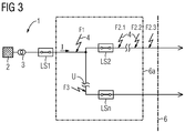
- FIG. 3 is the circuit arrangement of FIG. 1 shown with several possible shorts 4. The differences are that the shorts 4 should be present at different fault locations F.
- the circuit breaker LS2 is not yet open, so that in each case the back-up function of the circuit breaker LS1 is activated for the present below the threshold 6 possible short circuits, since the short-circuit current is large enough.
- the circuit breaker LS1 triggers for the short circuits 4 at the fault locations F1, F3 after the predetermined time, since these short circuits between the upstream and downstream circuit breakers LS1 and LS2, LSn are, and consequently none of the downstream circuit breaker LS1, LSn turns off.
- the circuit breaker LS1 In the case of the short circuits 4 at the fault locations F2.1, F2.2, F2.3, the circuit breaker LS1, after detecting the activation of its back-up function or after recognizing that the outgoing-side impedance is smaller than a predetermined threshold value, checks the time switch Course of the impedance, ie the ohmic resistance R. This has here an exponential but not by a switching arc 5 of a downstream circuit breaker LS2, LSn conditional on exponential history. He recognizes this by the fact that this exponential curve is not a given time value (here 1 ms) away from the zero crossing (since this is the case only with switching arcs 5).
- the circuit breaker LS2 responsible here does not pull a switching arc 5, ie it is not about to open, the circuit breaker LS1 opens (completely) after a predetermined current-dependent time has elapsed. Such a situation can occur, for example, in that the circuit breaker LS2 is defective.
- the circuit breaker LS1 is dependent on the activation of its back-up function, since the impedance measured by the circuit breaker LS1 is no longer in its impedance and thus effective range (ie the fault location F2.3 lies in the FIGS. 1 and 3 outside the area 6a).
Landscapes
- Keying Circuit Devices (AREA)
- Emergency Protection Circuit Devices (AREA)
Description
- Die Erfindung betrifft ein Verfahren zum selektiven Auslösen von einem vorgeordneten und mindestens einem diesem nachgeordneten Leistungsschalter gemäß dem Oberbegriff des Anspruchs 1.
- Es ist bekannt, Schutzgeräte in Form von Leistungsschaltern im Falle eines Kurzschlusses selektiv auszulösen. Dies bedeutet, dass jeweils der Leistungsschalter auslöst, welcher sich von der Stromeinspeisung aus gesehen am nächsten zum Kurzschluss befindet, so dass nicht mehr Verbraucher als unvermeidbar von der Abschaltung betroffen sind. Die einander vorund nachgeordneten Leistungsschalter unterliegen dazu einer Strom- und Zeitstaffelung; so weisen die einspeisenahen Leistungsschalter jeweils längere Abschaltzeiten als die nachgeordneten auf. Damit wird erreicht, dass die vorgeordneten Leistungsschalter nur dann eine Abschaltung vornehmen, wenn sie sich selbst am nächsten zum Kurzschluss befinden oder in Notfällen, wo ein nachgeordneter Leistungsschalter nicht auslöst, obwohl er auslösen müsste.
- Bei einer Strom- und Zeitstaffelung werden die Strom-Zeit-Kennlinien der Leistungsschalter so aufeinander abgestimmt, dass diese im Falle eines Kurzschlusses in Einspeiserichtung gesehen bei immer höheren Strömen und nach immer längeren Zeiten auslösen.
- Dies hat den Nachteil, dass die einspeisenahen Leistungsschalter relativ lange Abschaltzeiten aufweisen.
- Es ist bekannt, diese relativ langen Abschaltzeiten dadurch zu verkürzen, dass zwischen den Leistungsschaltern eine Kommunikationsverbindung hergestellt wird, mit deren Hilfe nachgeordnete Leistungsschalter den jeweils vorgeordneten Leistungsschaltern signalisieren, ob sie die Abschaltung vornehmen werden. Dafür ist allerdings ein zusätzlicher Verdrahtungsaufwand erforderlich.
- Aus der
WO 2006/108860 A1 ist ein Verfahren und eine Anordnung zur Erhöhung und Gewährleistung der Selektivität eines Schaltgerätes in einer Gruppe von Schaltgeräten sowie eine Verwendung der Anordnung beim Schalten in Stromkreisen bekannt. Bei einem Verfahren zur Erhöhung und Gewährleistung der Selektivität eines Schaltgerätes in einer Gruppe von Schaltgeraten, wobei der Schaltgerätegruppe wenigstens zwei Stromkreise mit einem ersten, vorgeordneten Schalter und wenigstens einem zweiten, nachgeordneten Schalter zugeordnet sind, werden folgende Maßnahmen durchgeführt: es wird die Impedanz des Stromkreises, der den nachgeordneten Schalter enthält, bestimmt und analysiert, zur Impedanzbestimmung werden die im Stromkreis des vorgeordneten Schalters vorhandenen Elemente des Stromkreises, wie Sammelschienen, Leitungen o. dgl., berücksichtigt, und durch die Impedanzanalyse wird die Selektivität verbessert. Bei der zugehörigen Anordnung zur Erhöhung und Gewährleistung der Selektivität eines Schaltgerätes in einer Gruppe von hintereinander geschalteten Schaltgeräten, wobei in der Schaltgerätegruppe wenigstens ein vorgeordneten Schalter und wenigstens ein nachgeordneten Schalter vorhanden sind, wird zur Selektivitätsbestimmung ein Mikroprozessor verwendet, wobei der Mikroprozessor im vorgeordneten Schalter angeordnet ist. - Die Aufgabe der Erfindung ist es, ein vereinfachtes Verfahren zum selektiven Auslösen anzugeben, das insbesondere auch bei den sehr kurzen Abschaltzeiten der Niederspannungs-Leistungsschalter anwendbar ist.
- Die Lösung ist durch die Merkmale des Patentanspruchs 1 gegeben; die Unteransprüche stellen vorteilhafte Ausgestaltungen dar.
- Die Lösung sieht vor, dass für den vorgeordneten Leistungsschalter der Schaltlichtbogen vorhanden ist, wenn der vom vorgeordneten Leistungsschalter aus gesehene abgangsseitige ohmsche Widerstand der vom Kurzschluss gebildeten Kurzschlussschleife zeitlich einen exponentiellen Verlauf aufweist. Mit dem Verfahren ist es also möglich, dass der vorgeordnete Leistungsschalter jeweils von sich aus feststellen kann, ob ein nachgeordneter Leistungsschalter einen Schaltlichtbogen erzeugt und damit, ob er bereits abschaltet. In diesem Falle kommt es nicht mehr zu einer dann unerwünschten Abschaltung durch den vorgeordneten Leistungsschalter. Vorteilhafterweise ist für diese Lösung kein zusätzlicher Schaltungsaufwand und auch keine Kommunikation der Leistungsschalter untereinander erforderlich.
- Um die Sicherheit beim Erfassen eines Schaltlichtbogens zu erhöhen, wird vorgeschlagen, zusätzlich zu prüfen, ob der exponentielle Verlauf vom Nulldurchgang des Wechselstroms jeweils weiter als ein vorgegebener Zeitwert entfernt verläuft.
- Bei Verwendung von Leistungsschaltern mit Back-up-Funktion, die große Kurzschlussströme durch Öffnen der Schaltkontakte ohne Betätigung des Schaltschlosses bereits selbsttätig begrenzen, wird vorgeschlagen, dass der vorgeordnete Leistungsschalter eine Back-up-Funktion aufweist und er diese Back-up-Funktion sowie die abgangsseitige Impedanz überwacht, dass erst nach Aktivierung der Back-up-Funktion und/oder wenn die abgangsseitige Impedanz innerhalb eines vorgegebenen Impedanzbereichs liegt das abgangsseitige Auftreten eines Schaltlichtbogens für eine vorgegebene Zeit überwacht wird und der vorgeordnete Leistungsschalter auslöst, wenn in der vorgegebenen Zeit kein Schaltlichtbogen auftritt.
- Alternativ ist es auch möglich, dass anstelle der abgangsseitigen Impedanz ein Strom-Schwellwert überwacht wird.
- Eine bessere Anpassung des Verfahrens wird erreicht, wenn die vorgegebene Zeit, vom Kurzschlusseintritt bis zum Erkennen eines nachgeordneten Schaltlichtbogens, stromabhängig ist.
- Die Erfindung wird nachfolgend anhand eines Ausführungsbeispiels näher beschrieben. Es zeigen:
- Figur 1
- eine schematische Darstellung einer Schaltungsanordnung mit mehreren Leistungsschaltern,
- Figur 2
- die Impedanz als Funktion der Zeit für die Schaltungsanordnung nach
Figur 1 bei einem Kurzschluss zum Zeitpunkt Null und - Figur 3
- die Schaltungsanordnung von
Figur 1 mit mehreren möglichen Kurzschlüssen an unterschiedlichen Orten. -
Figur 1 zeigt eine schematische Darstellung einer Schaltungsanordnung mit mehreren Schutzschaltern in Form von Leistungsschaltern LS, von denen in derFigur 1 nur drei Leistungsschalter LS1, LS2, LSn dargestellt sind. Bei den Leistungsschaltern LS handelt es sich um Strom begrenzende Niederspannungs-Leistungsschalter, die sehr kurze und von der Höhe des Kurzschlussstromes abhängige Abschaltzeiten aufweisen. Die Unterbrechung U dient der Vereinfachung der Darstellung der Schaltungsanordnung; sie besagt, dass zwischen den gezeigten Leistungsschaltern LS2 und LSn noch weitere Leistungsschalter LS vorhanden sein können. In derFigur 1 ist weiter eine Stromeinspeisung 1 gezeigt, zu der ein Stromnetz 2 sowie ein Transformator 3 gehören. Der Stromeinspeisung 1 folgt der (einspeisenahe) Leistungsschalter LS1, der den Leistungsschaltern LS2, LSn vorgeordnet ist. Dementsprechend sind die beiden Leistungsschalter LS2, LSn dem Leistungsschalter LS1 nachgeordnet. "Vorgeordnet" und "nachgeordnet" sind jeweils von der Stromeinspeisung 1 aus gesehen definiert. - Ein Pfeil am Fehlerort F2.5 soll anzeigen, dass dort ein Kurzschluss 4 vorliegt. Die
Figur 1 zeigt weiter, dass der dem Fehlerort F2.5 am nächsten liegende Leistungsschalter LS2 bereits dabei ist zu öffnen und damit die vom Kurzschluss 4 gebildete Kurzschlussschleife von der Stromeinspeisung 1 zu trennen. Dabei ziehen die sich öffnenden Schaltkontakte des Leistungsschalters LS2 einen inFigur 1 gezeigten Schaltlichtbogen 5, der bei einer weiteren Öffnung der Schaltkontakte gelöscht wird und folglich bei vollständig geöffneten Schaltkontakten wieder erloschen ist. - Der Leistungsschalter LS1 besitzt eine Back-up-Funktion, d.h. er öffnet ebenfalls etwas (zusammen mit dem Leistungsschalter LS2), wenn sich der Kurzschluss 4 von der Stromeinspeisung 1 aus gesehen vor seiner Ansprechschwelle 6 befindet und der Kurzschlussstrom einen Mindestwert überschritten hat. Durch die Back-up-Funktion des Leistungsschalters LS1 wird der fließende Strom I bereits begrenzt.
- In der
Figur 1 befindet sich der Kurzschluss 4 nicht vor sondern hinter der Ansprechschwelle 6, so dass die Back-up-Funktion des Leistungsschalters LS1 nicht aktiv ist. Weiter befindet sich der Kurzschluss 4 und die Ansprechschwelle 6 innerhalb eines Bereichs 6a, welcher schematisch den Schutz- bzw. Wirkungsbereich des einspeisenahen Leistungsschalters LS1 angibt, d.h. in dem sich die abgangsseitige Impedanz R (s.Figur 2 ) bei Auftreten eines Kurzschlusses 4 signifikant ändert. - Der vorgeordnete Leistungsschalter LS1 beobachtet (überwacht) jeweils seine Back-up-Funktion (z.B. mittels Photodioden oder Bewegungssensoren) und die abgangsseitige Impedanz, d.h. die vom Leistungsschalter LS1 in Richtung der Leistungsschalter LS2, LSn vorliegende Impedanz. Sie weist einen ohmschen Anteil (ohmscher Widerstand R in
Figur 2 ) als auch einen imaginären Anteil auf. Durch den Kurzschluss 4 verkleinert sich die abgangsseitige Impedanz, da durch den Kurzschluss 4 innerhalb der Schaltungsanordnung eine Kurzschlussschleife entsteht. Der Leistungsschalter LS1 überwacht hier, ob die abgangsseitige Impedanz kleiner als ein vorgegebener Schwellwert ist. Die Überwachung kann aber auch prüfen, ob die Impedanz jeweils innerhalb eines vorgegebenen Impedanzbereichs liegt. In der Schaltungsanordnung inFigur 1 hat die abgangsseitige Impedanz den vorgegebenen Schwellwert unterschritten und vom Zeitpunkt des Unterschreitens an prüft der Leistungsschalter LS1 den abgangsseitigen ohmschen Widerstand R auf exponentiellen Verlauf. -
Figur 2 zeigt den ohmschen Anteil (ohmschen Widerstand R) der Impedanz als Funktion der Zeit t für die Schaltungsanordnung gemäßFigur 1 . Der Verlauf des abgangsseitigen ohmschen Widerstands R ist dabei aufgrund des Schaltlichtbogens 5 exponentiell (logarithmische Einteilung der Ordinate oder R-Achse inFigur 2 ) und bricht dann bei 9 ms ab, wobei der unbeeinflusste Wechselstrom I bei 10 ms jeweils seinen Nulldurchgang hätte. - Der Leistungsschalter LS1 prüft, ob der Verlauf des ohmschen Widerstands R exponentiell ist und zusätzlich bis zu einem vorgegebenen Zeitwert (hier 1 ms) vom Nulldurchgang entfernt verläuft, was in
Figur 2 der Fall ist. - Andere Störungen können ebenfalls einen exponentiellen Impedanzverlauf bewirken. Allerdings hat sich gezeigt, dass ein von Störungen hervorgerufener exponentieller Impedanzverlauf an den Nulldurchgängen des Wechselstroms I regelmäßig nicht abbricht, sondern vorzugsweise während der Nulldurchgänge vorhanden ist.
- In
Figur 1 erkennt der Leistungsschalter LS1 anhand des exponentiellen Verlaufs des ohmschen Widerstands R und der Entfernung von mehr als 1 ms vom Nulldurchgang, dass ein Schaltlichtbogen 5 vorhanden ist und er folglich nicht selbst öffnen (abschalten) muss, da ein nachgeordneter Leistungsschalter (hier der Leistungsschalter LS2) bereits dabei ist, zu öffnen. - In
Figur 3 ist die Schaltungsanordnung vonFigur 1 mit mehreren möglichen Kurzschlüssen 4 gezeigt. Die Unterschiede bestehen darin, dass die Kurzschlüsse 4 an unterschiedlichen Fehlerorten F vorhanden sein sollen. Außerdem ist der Leistungsschalter LS2 noch nicht dabei zu öffnen, so dass für die unterhalb der Ansprechschwelle 6 vorhandenen möglichen Kurzschlüsse jeweils die Back-up-Funktion des Leistungsschalters LS1 aktiviert wird, da der Kurzschlussstrom groß genug ist. - Der Leistungsschalter LS1 löst für die Kurzschlüsse 4 an den Fehlerorten F1, F3 nach der vorgegebenen Zeit aus, da diese Kurzschlüsse zwischen dem vorgeordneten und den nachgeordneten Leistungsschaltern LS1 bzw. LS2, LSn liegen und folglich keiner der nachgeordneten Leistungsschalter LS1, LSn abschaltet.
- Bei den Kurzschlüssen 4 an den Fehlerorten F2.1, F2.2, F2.3 prüft der Leistungsschalter LS1 nach Erkennen der Aktivierung seiner Back-up-Funktion bzw. nach Erkennen, dass die abgangsseitige Impedanz kleiner als ein vorgegebener Schwellwert ist, den zeitlichen Verlauf der Impedanz, d.h. den ohmschen Widerstand R. Dieser weist hier einen exponentiellen aber keinen durch einen Schaltlichtbogen 5 eines nachgeordneten Leistungsschalters LS2, LSn bedingten exponentiellen Verlauf auf. Das erkennt er hier dadurch, dass dieser exponentiellen Verlauf nicht einen vorgegebenen zeitwert (hier 1 ms) vom Nulldurchgang entfernt verläuft (da dies nur bei Schaltlichtbögen 5 der Fall ist). Wenn der hier zuständige Leistungsschalter LS2 keinen Schaltlichtbogen 5 zieht, er also nicht dabei ist zu öffnen, öffnet der Leistungsschalter LS1 nach Ablauf einer vorgegebenen stromabhängigen Zeit (vollständig). Eine solche Situation kann beispielsweise dadurch eintreten, dass der Leistungsschalter LS2 defekt ist.
- Zieht der Leistungsschalter LS2 dagegen innerhalb der vorgegebenen Zeit einen Schaltlichtbogen 5 (in
Figur 3 nicht dargestellt), so würde dieser vom Leistungsschalter LS1 erkannt und der Leistungsschalter LS1 würde nicht auslösen, sondern nur der Leistungsschalter LS2. - Für den Fehlerort F2.3 ist der Leistungsschalter LS1 auf die Aktivierung seiner Back-up-Funktion angewiesen, da die vom Leistungsschalter LS1 gemessene Impedanz nicht mehr in dessen Impedanz- und somit Wirkungsbereich liegt (d.h. der Fehlerort F2.3 liegt in den
Figuren 1 und3 außerhalb des Bereichs 6a).
Claims (4)
- Verfahren zum selektiven Auslösen von einem vorgeordneten Leistungsschalter (LS1) und mindestens einem diesem nachgeordneten Leistungsschalter (LS2, LSn),
wobei der vorgeordnete Leistungsschalter (LS1) überwacht, ob der mindestens eine nachgeordnete Leistungsschalter (LS2, LSn) als Folge eines hinter dem nachgeordneten Leistungsschalter (LS2, LSn) aufgetretenen Kurzschlusses (4) bereits unter Bildung eines Schaltlichtbogens (5) dabei ist zu öffnen, und
bei dem der vorgeordnete Leistungsschalter (LS1) selbst nicht auslöst, wenn er abgangsseitig den Schaltlichtbogen (5) erkennt,
dadurch gekennzeichnet,
dass für den vorgeordneten Leistungsschalter (LS1) der Schaltlichtbogen (5) vorhanden ist, wenn der vom vorgeordneten Leistungsschalter (LS1) aus gesehene abgangsseitige ohmsche Widerstand (R) der vom Kurzschluss (4) gebildeten Kurzschlussschleife zeitlich einen exponentiellen Verlauf aufweist. - Verfahren nach Anspruch 1,
dadurch gekennzeichnet,
dass dieser exponentielle Verlauf vom Nulldurchgang des Wechselstroms (I) jeweils weiter als ein vorgegebener zeitwert entfernt verläuft. - Verfahren nach Anspruch 1 oder 2,
dadurch gekennzeichnet,
dass der vorgeordnete Leistungsschalter (LS1) eine Back-up-Funktion aufweist und er diese Back-up-Funktion sowie die abgangsseitige Impedanz überwacht,
dass erst nach Aktivierung der Back-up-Funktion und/oder wenn die abgangsseitige Impedanz innerhalb eines vorgegebenen Impedanzbereichs liegt das abgangsseitige Auftreten eines Schaltlichtbogens (5) für eine vorgegebene Zeit überwacht wird und der vorgeordnete Leistungsschalter (LS1) auslöst, wenn in der vorgegebenen Zeit kein Schaltlichtbogen (5) auftritt. - Verfahren nach Anspruch 3,
dadurch gekennzeichnet,
dass die vorgegebene Zeit stromabhängig ist.
Applications Claiming Priority (2)
| Application Number | Priority Date | Filing Date | Title |
|---|---|---|---|
| DE200710021270 DE102007021270A1 (de) | 2007-05-03 | 2007-05-03 | Verfahren zum selektiven Auslösen von Leistungsschaltern |
| PCT/EP2008/055310 WO2008135479A1 (de) | 2007-05-03 | 2008-04-30 | Verfahren zum selektiven auslösen von leistungsschaltern |
Publications (2)
| Publication Number | Publication Date |
|---|---|
| EP2143184A1 EP2143184A1 (de) | 2010-01-13 |
| EP2143184B1 true EP2143184B1 (de) | 2016-06-15 |
Family
ID=39707947
Family Applications (1)
| Application Number | Title | Priority Date | Filing Date |
|---|---|---|---|
| EP08736632.4A Not-in-force EP2143184B1 (de) | 2007-05-03 | 2008-04-30 | Verfahren zum selektiven auslösen von leistungsschaltern |
Country Status (3)
| Country | Link |
|---|---|
| EP (1) | EP2143184B1 (de) |
| DE (1) | DE102007021270A1 (de) |
| WO (1) | WO2008135479A1 (de) |
Families Citing this family (4)
| Publication number | Priority date | Publication date | Assignee | Title |
|---|---|---|---|---|
| DE102010042609A1 (de) * | 2010-10-19 | 2012-04-19 | Siemens Aktiengesellschaft | Verfahren für eine Anordnung zur Stromverteilung mit einer Einspeisung und nachfolgend mindestens zwei Schaltern mit selektiven Eigenschaften |
| DE102011082339A1 (de) * | 2011-09-08 | 2013-03-14 | Siemens Aktiengesellschaft | Anordnung zur Stromverteilung mit zwei miteinander verbundenen Schaltern, insbesondere Leistungsschaltern für Niederspannungen |
| DE102016209443B4 (de) * | 2016-05-31 | 2021-06-10 | Siemens Aktiengesellschaft | Störlichtbogenerkennungseinheit |
| DE102022202653A1 (de) * | 2022-03-17 | 2023-09-21 | Siemens Aktiengesellschaft | Verfahren zum Backup-Schutz |
Family Cites Families (2)
| Publication number | Priority date | Publication date | Assignee | Title |
|---|---|---|---|---|
| FR2791823B1 (fr) * | 1999-03-30 | 2001-05-11 | Electricite De France | Dispositif et procede de protection d'une ligne d'un reseau de lignes d'alimentation en energie electrique |
| EP1869746A1 (de) * | 2005-04-15 | 2007-12-26 | Siemens Aktiengesellschaft | Verfahren und anordnung zur erhöhung und gewährleistung der selektivität eines schaltgerätes in einer gruppe von schaltgeräten sowie verwendung der anordnung beim schalten in stromkreisen |
-
2007
- 2007-05-03 DE DE200710021270 patent/DE102007021270A1/de not_active Withdrawn
-
2008
- 2008-04-30 WO PCT/EP2008/055310 patent/WO2008135479A1/de not_active Ceased
- 2008-04-30 EP EP08736632.4A patent/EP2143184B1/de not_active Not-in-force
Also Published As
| Publication number | Publication date |
|---|---|
| WO2008135479A1 (de) | 2008-11-13 |
| DE102007021270A1 (de) | 2008-11-06 |
| EP2143184A1 (de) | 2010-01-13 |
Similar Documents
| Publication | Publication Date | Title |
|---|---|---|
| EP2291895B1 (de) | Verfahren zum selektiven auslösen von leistungsschaltern im falle eines kurzschlusses | |
| DE102014204038A1 (de) | Verfahren und Vorrichtungen zur selektiven Isolationsüberwachung in ungeerdeten IT-Stromversorgungssystemen | |
| DE102014005524B4 (de) | Unterbrechung eines Stromes | |
| EP1386381A1 (de) | Leistungsschalter mit elektronischem auslöser und bypass-schaltung | |
| EP3555982B1 (de) | Überstrom- und kurzschlussdetektor | |
| DE102010063419A1 (de) | Verfahren zum Detektieren von Störlichtbogenereignissen durch einen Fehlerzähler und Vorrichtung | |
| EP2549612A2 (de) | Verfahren zum Sperren eines Schalters | |
| AT503541A1 (de) | Schalteinrichtung | |
| EP2143184B1 (de) | Verfahren zum selektiven auslösen von leistungsschaltern | |
| DE10032655A1 (de) | Elektrischer Überstromauslöser für einen Niederspannungs-Leistungsschalter | |
| DE69832654T2 (de) | Selektiver elektronischer Auslöser, Lastschalter mit einem solchen Auslöser und ein selektives Auslöseverfahren | |
| DE102011120466B4 (de) | Elektronischer Schutzschalter und Verfahren zur Betätigung des Schutzschalters | |
| DE69122078T2 (de) | Leistungseinführungssystem | |
| DE102010042609A1 (de) | Verfahren für eine Anordnung zur Stromverteilung mit einer Einspeisung und nachfolgend mindestens zwei Schaltern mit selektiven Eigenschaften | |
| DE102011005563B4 (de) | Verfahren und Vorrichtung zur Umschaltung von Stromeinspeisungen | |
| EP3347959B1 (de) | Anordnung zur sicheren, von schaltgeräten oder vorsicherungen unabhängigen, netzseitigen abtrennung von überspannungsschutzeinrichtungen im fall kritischer betriebszustände | |
| DE10117372B4 (de) | Schutzeinrichtung, Schutzanordnung und Schutzverfahren für eine elektrische Leitung | |
| EP2548214B1 (de) | Fehlerstromschutzschalter | |
| EP0848471A2 (de) | Fehlerstromschutzeinrichtung | |
| EP2672595B1 (de) | Schaltungsanordnung und Verfahren zur Gleichstromunterbrechung | |
| DE102011082342A1 (de) | Anordnung zur Stromverteilung mit zwei miteinander verbundenen Schaltern, insbesondere Leistungsschaltern für Niederspannungen | |
| DE19927030A1 (de) | Leistungsschalter mit einem elektronischen, mikroprozessorgesteuerten Auslöser und einer Bypass-Schaltung | |
| DE102011080826A1 (de) | Verfahren zum Ermitteln der Lichtbogenleistung eines Schalters, Verfahren zum Auslösen eines Schalters anhand der Lichtbogenleistung und Verfahren zur Ermittlung der Belastung der Kontakte eines Schalters anhand der Lichtbogenenergie | |
| DE102011082339A1 (de) | Anordnung zur Stromverteilung mit zwei miteinander verbundenen Schaltern, insbesondere Leistungsschaltern für Niederspannungen | |
| DE10062280A1 (de) | Sicherheitsschaltung für eine elektrische und/oder elektronische Steuerungsschaltung eines elektrischen Gerätes |
Legal Events
| Date | Code | Title | Description |
|---|---|---|---|
| PUAI | Public reference made under article 153(3) epc to a published international application that has entered the european phase |
Free format text: ORIGINAL CODE: 0009012 |
|
| 17P | Request for examination filed |
Effective date: 20091023 |
|
| AK | Designated contracting states |
Kind code of ref document: A1 Designated state(s): AT BE BG CH CY CZ DE DK EE ES FI FR GB GR HR HU IE IS IT LI LT LU LV MC MT NL NO PL PT RO SE SI SK TR |
|
| DAX | Request for extension of the european patent (deleted) | ||
| RAP1 | Party data changed (applicant data changed or rights of an application transferred) |
Owner name: SIEMENS AKTIENGESELLSCHAFT |
|
| 17Q | First examination report despatched |
Effective date: 20150323 |
|
| GRAP | Despatch of communication of intention to grant a patent |
Free format text: ORIGINAL CODE: EPIDOSNIGR1 |
|
| RIC1 | Information provided on ipc code assigned before grant |
Ipc: H02H 7/26 20060101AFI20151207BHEP Ipc: H02H 7/30 20060101ALI20151207BHEP |
|
| INTG | Intention to grant announced |
Effective date: 20160107 |
|
| GRAS | Grant fee paid |
Free format text: ORIGINAL CODE: EPIDOSNIGR3 |
|
| GRAA | (expected) grant |
Free format text: ORIGINAL CODE: 0009210 |
|
| AK | Designated contracting states |
Kind code of ref document: B1 Designated state(s): AT BE BG CH CY CZ DE DK EE ES FI FR GB GR HR HU IE IS IT LI LT LU LV MC MT NL NO PL PT RO SE SI SK TR |
|
| REG | Reference to a national code |
Ref country code: CH Ref legal event code: EP Ref country code: GB Ref legal event code: FG4D Free format text: NOT ENGLISH |
|
| REG | Reference to a national code |
Ref country code: IE Ref legal event code: FG4D Free format text: LANGUAGE OF EP DOCUMENT: GERMAN |
|
| REG | Reference to a national code |
Ref country code: AT Ref legal event code: REF Ref document number: 806940 Country of ref document: AT Kind code of ref document: T Effective date: 20160715 |
|
| REG | Reference to a national code |
Ref country code: DE Ref legal event code: R096 Ref document number: 502008014304 Country of ref document: DE |
|
| REG | Reference to a national code |
Ref country code: LT Ref legal event code: MG4D |
|
| REG | Reference to a national code |
Ref country code: NL Ref legal event code: MP Effective date: 20160615 |
|
| PG25 | Lapsed in a contracting state [announced via postgrant information from national office to epo] |
Ref country code: NO Free format text: LAPSE BECAUSE OF FAILURE TO SUBMIT A TRANSLATION OF THE DESCRIPTION OR TO PAY THE FEE WITHIN THE PRESCRIBED TIME-LIMIT Effective date: 20160915 Ref country code: LT Free format text: LAPSE BECAUSE OF FAILURE TO SUBMIT A TRANSLATION OF THE DESCRIPTION OR TO PAY THE FEE WITHIN THE PRESCRIBED TIME-LIMIT Effective date: 20160615 Ref country code: FI Free format text: LAPSE BECAUSE OF FAILURE TO SUBMIT A TRANSLATION OF THE DESCRIPTION OR TO PAY THE FEE WITHIN THE PRESCRIBED TIME-LIMIT Effective date: 20160615 |
|
| PG25 | Lapsed in a contracting state [announced via postgrant information from national office to epo] |
Ref country code: GR Free format text: LAPSE BECAUSE OF FAILURE TO SUBMIT A TRANSLATION OF THE DESCRIPTION OR TO PAY THE FEE WITHIN THE PRESCRIBED TIME-LIMIT Effective date: 20160916 Ref country code: NL Free format text: LAPSE BECAUSE OF FAILURE TO SUBMIT A TRANSLATION OF THE DESCRIPTION OR TO PAY THE FEE WITHIN THE PRESCRIBED TIME-LIMIT Effective date: 20160615 Ref country code: LV Free format text: LAPSE BECAUSE OF FAILURE TO SUBMIT A TRANSLATION OF THE DESCRIPTION OR TO PAY THE FEE WITHIN THE PRESCRIBED TIME-LIMIT Effective date: 20160615 Ref country code: HR Free format text: LAPSE BECAUSE OF FAILURE TO SUBMIT A TRANSLATION OF THE DESCRIPTION OR TO PAY THE FEE WITHIN THE PRESCRIBED TIME-LIMIT Effective date: 20160615 Ref country code: SE Free format text: LAPSE BECAUSE OF FAILURE TO SUBMIT A TRANSLATION OF THE DESCRIPTION OR TO PAY THE FEE WITHIN THE PRESCRIBED TIME-LIMIT Effective date: 20160615 |
|
| PG25 | Lapsed in a contracting state [announced via postgrant information from national office to epo] |
Ref country code: EE Free format text: LAPSE BECAUSE OF FAILURE TO SUBMIT A TRANSLATION OF THE DESCRIPTION OR TO PAY THE FEE WITHIN THE PRESCRIBED TIME-LIMIT Effective date: 20160615 Ref country code: CZ Free format text: LAPSE BECAUSE OF FAILURE TO SUBMIT A TRANSLATION OF THE DESCRIPTION OR TO PAY THE FEE WITHIN THE PRESCRIBED TIME-LIMIT Effective date: 20160615 Ref country code: SK Free format text: LAPSE BECAUSE OF FAILURE TO SUBMIT A TRANSLATION OF THE DESCRIPTION OR TO PAY THE FEE WITHIN THE PRESCRIBED TIME-LIMIT Effective date: 20160615 Ref country code: RO Free format text: LAPSE BECAUSE OF FAILURE TO SUBMIT A TRANSLATION OF THE DESCRIPTION OR TO PAY THE FEE WITHIN THE PRESCRIBED TIME-LIMIT Effective date: 20160615 Ref country code: IS Free format text: LAPSE BECAUSE OF FAILURE TO SUBMIT A TRANSLATION OF THE DESCRIPTION OR TO PAY THE FEE WITHIN THE PRESCRIBED TIME-LIMIT Effective date: 20161015 |
|
| PG25 | Lapsed in a contracting state [announced via postgrant information from national office to epo] |
Ref country code: PT Free format text: LAPSE BECAUSE OF FAILURE TO SUBMIT A TRANSLATION OF THE DESCRIPTION OR TO PAY THE FEE WITHIN THE PRESCRIBED TIME-LIMIT Effective date: 20161017 Ref country code: PL Free format text: LAPSE BECAUSE OF FAILURE TO SUBMIT A TRANSLATION OF THE DESCRIPTION OR TO PAY THE FEE WITHIN THE PRESCRIBED TIME-LIMIT Effective date: 20160615 Ref country code: ES Free format text: LAPSE BECAUSE OF FAILURE TO SUBMIT A TRANSLATION OF THE DESCRIPTION OR TO PAY THE FEE WITHIN THE PRESCRIBED TIME-LIMIT Effective date: 20160615 |
|
| REG | Reference to a national code |
Ref country code: DE Ref legal event code: R097 Ref document number: 502008014304 Country of ref document: DE |
|
| PLBE | No opposition filed within time limit |
Free format text: ORIGINAL CODE: 0009261 |
|
| STAA | Information on the status of an ep patent application or granted ep patent |
Free format text: STATUS: NO OPPOSITION FILED WITHIN TIME LIMIT |
|
| REG | Reference to a national code |
Ref country code: FR Ref legal event code: PLFP Year of fee payment: 10 |
|
| 26N | No opposition filed |
Effective date: 20170316 |
|
| PG25 | Lapsed in a contracting state [announced via postgrant information from national office to epo] |
Ref country code: DK Free format text: LAPSE BECAUSE OF FAILURE TO SUBMIT A TRANSLATION OF THE DESCRIPTION OR TO PAY THE FEE WITHIN THE PRESCRIBED TIME-LIMIT Effective date: 20160615 |
|
| PG25 | Lapsed in a contracting state [announced via postgrant information from national office to epo] |
Ref country code: SI Free format text: LAPSE BECAUSE OF FAILURE TO SUBMIT A TRANSLATION OF THE DESCRIPTION OR TO PAY THE FEE WITHIN THE PRESCRIBED TIME-LIMIT Effective date: 20160615 |
|
| REG | Reference to a national code |
Ref country code: CH Ref legal event code: NV Representative=s name: SIEMENS SCHWEIZ AG, CH Ref country code: CH Ref legal event code: PCOW Free format text: NEW ADDRESS: WERNER-VON-SIEMENS-STRASSE 1, 80333 MUENCHEN (DE) |
|
| REG | Reference to a national code |
Ref country code: CH Ref legal event code: PL |
|
| GBPC | Gb: european patent ceased through non-payment of renewal fee |
Effective date: 20170430 |
|
| REG | Reference to a national code |
Ref country code: IE Ref legal event code: MM4A |
|
| PG25 | Lapsed in a contracting state [announced via postgrant information from national office to epo] |
Ref country code: MC Free format text: LAPSE BECAUSE OF FAILURE TO SUBMIT A TRANSLATION OF THE DESCRIPTION OR TO PAY THE FEE WITHIN THE PRESCRIBED TIME-LIMIT Effective date: 20160615 |
|
| PG25 | Lapsed in a contracting state [announced via postgrant information from national office to epo] |
Ref country code: GB Free format text: LAPSE BECAUSE OF NON-PAYMENT OF DUE FEES Effective date: 20170430 Ref country code: CH Free format text: LAPSE BECAUSE OF NON-PAYMENT OF DUE FEES Effective date: 20170430 Ref country code: LI Free format text: LAPSE BECAUSE OF NON-PAYMENT OF DUE FEES Effective date: 20170430 Ref country code: LU Free format text: LAPSE BECAUSE OF NON-PAYMENT OF DUE FEES Effective date: 20170430 |
|
| REG | Reference to a national code |
Ref country code: BE Ref legal event code: MM Effective date: 20170430 |
|
| REG | Reference to a national code |
Ref country code: FR Ref legal event code: PLFP Year of fee payment: 11 |
|
| PG25 | Lapsed in a contracting state [announced via postgrant information from national office to epo] |
Ref country code: IE Free format text: LAPSE BECAUSE OF NON-PAYMENT OF DUE FEES Effective date: 20170430 |
|
| PG25 | Lapsed in a contracting state [announced via postgrant information from national office to epo] |
Ref country code: BE Free format text: LAPSE BECAUSE OF NON-PAYMENT OF DUE FEES Effective date: 20170430 |
|
| REG | Reference to a national code |
Ref country code: AT Ref legal event code: MM01 Ref document number: 806940 Country of ref document: AT Kind code of ref document: T Effective date: 20170430 |
|
| PG25 | Lapsed in a contracting state [announced via postgrant information from national office to epo] |
Ref country code: AT Free format text: LAPSE BECAUSE OF NON-PAYMENT OF DUE FEES Effective date: 20170430 |
|
| PGFP | Annual fee paid to national office [announced via postgrant information from national office to epo] |
Ref country code: IT Payment date: 20180423 Year of fee payment: 11 Ref country code: FR Payment date: 20180412 Year of fee payment: 11 |
|
| PG25 | Lapsed in a contracting state [announced via postgrant information from national office to epo] |
Ref country code: MT Free format text: LAPSE BECAUSE OF FAILURE TO SUBMIT A TRANSLATION OF THE DESCRIPTION OR TO PAY THE FEE WITHIN THE PRESCRIBED TIME-LIMIT Effective date: 20160615 |
|
| PG25 | Lapsed in a contracting state [announced via postgrant information from national office to epo] |
Ref country code: HU Free format text: LAPSE BECAUSE OF FAILURE TO SUBMIT A TRANSLATION OF THE DESCRIPTION OR TO PAY THE FEE WITHIN THE PRESCRIBED TIME-LIMIT; INVALID AB INITIO Effective date: 20080430 |
|
| PGFP | Annual fee paid to national office [announced via postgrant information from national office to epo] |
Ref country code: DE Payment date: 20190617 Year of fee payment: 12 |
|
| PG25 | Lapsed in a contracting state [announced via postgrant information from national office to epo] |
Ref country code: BG Free format text: LAPSE BECAUSE OF FAILURE TO SUBMIT A TRANSLATION OF THE DESCRIPTION OR TO PAY THE FEE WITHIN THE PRESCRIBED TIME-LIMIT Effective date: 20160615 |
|
| PG25 | Lapsed in a contracting state [announced via postgrant information from national office to epo] |
Ref country code: CY Free format text: LAPSE BECAUSE OF NON-PAYMENT OF DUE FEES Effective date: 20160615 |
|
| PG25 | Lapsed in a contracting state [announced via postgrant information from national office to epo] |
Ref country code: TR Free format text: LAPSE BECAUSE OF FAILURE TO SUBMIT A TRANSLATION OF THE DESCRIPTION OR TO PAY THE FEE WITHIN THE PRESCRIBED TIME-LIMIT Effective date: 20160615 |
|
| PG25 | Lapsed in a contracting state [announced via postgrant information from national office to epo] |
Ref country code: IT Free format text: LAPSE BECAUSE OF NON-PAYMENT OF DUE FEES Effective date: 20190430 |
|
| PG25 | Lapsed in a contracting state [announced via postgrant information from national office to epo] |
Ref country code: FR Free format text: LAPSE BECAUSE OF NON-PAYMENT OF DUE FEES Effective date: 20190430 |
|
| REG | Reference to a national code |
Ref country code: DE Ref legal event code: R119 Ref document number: 502008014304 Country of ref document: DE |
|
| PG25 | Lapsed in a contracting state [announced via postgrant information from national office to epo] |
Ref country code: DE Free format text: LAPSE BECAUSE OF NON-PAYMENT OF DUE FEES Effective date: 20201103 |