EP2144034A1 - Procédé de mesure de structure multicouches et appareil de mesure de structure multicouches - Google Patents
Procédé de mesure de structure multicouches et appareil de mesure de structure multicouches Download PDFInfo
- Publication number
- EP2144034A1 EP2144034A1 EP09163477A EP09163477A EP2144034A1 EP 2144034 A1 EP2144034 A1 EP 2144034A1 EP 09163477 A EP09163477 A EP 09163477A EP 09163477 A EP09163477 A EP 09163477A EP 2144034 A1 EP2144034 A1 EP 2144034A1
- Authority
- EP
- European Patent Office
- Prior art keywords
- light
- optical distance
- layer
- multilayer structure
- wave
- Prior art date
- Legal status (The legal status is an assumption and is not a legal conclusion. Google has not performed a legal analysis and makes no representation as to the accuracy of the status listed.)
- Withdrawn
Links
- 238000000034 method Methods 0.000 title claims abstract description 32
- 230000003287 optical effect Effects 0.000 claims abstract description 139
- 238000001228 spectrum Methods 0.000 claims abstract description 34
- 238000005259 measurement Methods 0.000 claims description 50
- 238000001514 detection method Methods 0.000 claims description 15
- 238000004458 analytical method Methods 0.000 claims description 7
- 238000000605 extraction Methods 0.000 claims description 2
- 239000010410 layer Substances 0.000 description 81
- 230000014509 gene expression Effects 0.000 description 37
- 238000010276 construction Methods 0.000 description 19
- 230000003595 spectral effect Effects 0.000 description 18
- 239000010408 film Substances 0.000 description 15
- 239000006185 dispersion Substances 0.000 description 9
- 210000001508 eye Anatomy 0.000 description 9
- 210000001525 retina Anatomy 0.000 description 9
- 230000001066 destructive effect Effects 0.000 description 8
- 238000012014 optical coherence tomography Methods 0.000 description 8
- 238000012545 processing Methods 0.000 description 8
- 238000005070 sampling Methods 0.000 description 8
- 238000010586 diagram Methods 0.000 description 6
- 239000011521 glass Substances 0.000 description 6
- 230000006870 function Effects 0.000 description 4
- 239000000758 substrate Substances 0.000 description 4
- 238000003384 imaging method Methods 0.000 description 3
- 239000004065 semiconductor Substances 0.000 description 3
- 230000008859 change Effects 0.000 description 2
- 238000006243 chemical reaction Methods 0.000 description 2
- 230000001427 coherent effect Effects 0.000 description 2
- 230000005684 electric field Effects 0.000 description 2
- 229910052736 halogen Inorganic materials 0.000 description 2
- 150000002367 halogens Chemical class 0.000 description 2
- 230000010287 polarization Effects 0.000 description 2
- 238000002310 reflectometry Methods 0.000 description 2
- 238000010408 sweeping Methods 0.000 description 2
- 238000002834 transmittance Methods 0.000 description 2
- 101000802640 Homo sapiens Lactosylceramide 4-alpha-galactosyltransferase Proteins 0.000 description 1
- 102100035838 Lactosylceramide 4-alpha-galactosyltransferase Human genes 0.000 description 1
- 229910052581 Si3N4 Inorganic materials 0.000 description 1
- XUIMIQQOPSSXEZ-UHFFFAOYSA-N Silicon Chemical compound [Si] XUIMIQQOPSSXEZ-UHFFFAOYSA-N 0.000 description 1
- 238000000149 argon plasma sintering Methods 0.000 description 1
- 210000005252 bulbus oculi Anatomy 0.000 description 1
- 238000007796 conventional method Methods 0.000 description 1
- 210000004087 cornea Anatomy 0.000 description 1
- 238000013461 design Methods 0.000 description 1
- 230000006866 deterioration Effects 0.000 description 1
- 239000000835 fiber Substances 0.000 description 1
- 238000001914 filtration Methods 0.000 description 1
- 230000006872 improvement Effects 0.000 description 1
- 230000001678 irradiating effect Effects 0.000 description 1
- 239000000463 material Substances 0.000 description 1
- 230000007246 mechanism Effects 0.000 description 1
- 238000012986 modification Methods 0.000 description 1
- 230000004048 modification Effects 0.000 description 1
- 229910052710 silicon Inorganic materials 0.000 description 1
- 239000010703 silicon Substances 0.000 description 1
- HQVNEWCFYHHQES-UHFFFAOYSA-N silicon nitride Chemical compound N12[Si]34N5[Si]62N3[Si]51N64 HQVNEWCFYHHQES-UHFFFAOYSA-N 0.000 description 1
- 239000002356 single layer Substances 0.000 description 1
- 230000002269 spontaneous effect Effects 0.000 description 1
- 239000010409 thin film Substances 0.000 description 1
- 230000001131 transforming effect Effects 0.000 description 1
Images



Classifications
-
- A—HUMAN NECESSITIES
- A61—MEDICAL OR VETERINARY SCIENCE; HYGIENE
- A61B—DIAGNOSIS; SURGERY; IDENTIFICATION
- A61B3/00—Apparatus for testing the eyes; Instruments for examining the eyes
- A61B3/10—Objective types, i.e. instruments for examining the eyes independent of the patients' perceptions or reactions
- A61B3/1005—Objective types, i.e. instruments for examining the eyes independent of the patients' perceptions or reactions for measuring distances inside the eye, e.g. thickness of the cornea
-
- A—HUMAN NECESSITIES
- A61—MEDICAL OR VETERINARY SCIENCE; HYGIENE
- A61B—DIAGNOSIS; SURGERY; IDENTIFICATION
- A61B3/00—Apparatus for testing the eyes; Instruments for examining the eyes
- A61B3/10—Objective types, i.e. instruments for examining the eyes independent of the patients' perceptions or reactions
- A61B3/102—Objective types, i.e. instruments for examining the eyes independent of the patients' perceptions or reactions for optical coherence tomography [OCT]
-
- G—PHYSICS
- G01—MEASURING; TESTING
- G01B—MEASURING LENGTH, THICKNESS OR SIMILAR LINEAR DIMENSIONS; MEASURING ANGLES; MEASURING AREAS; MEASURING IRREGULARITIES OF SURFACES OR CONTOURS
- G01B11/00—Measuring arrangements characterised by the use of optical techniques
- G01B11/02—Measuring arrangements characterised by the use of optical techniques for measuring length, width or thickness
- G01B11/06—Measuring arrangements characterised by the use of optical techniques for measuring length, width or thickness for measuring thickness ; e.g. of sheet material
- G01B11/0616—Measuring arrangements characterised by the use of optical techniques for measuring length, width or thickness for measuring thickness ; e.g. of sheet material of coating
- G01B11/0625—Measuring arrangements characterised by the use of optical techniques for measuring length, width or thickness for measuring thickness ; e.g. of sheet material of coating with measurement of absorption or reflection
-
- G—PHYSICS
- G01—MEASURING; TESTING
- G01B—MEASURING LENGTH, THICKNESS OR SIMILAR LINEAR DIMENSIONS; MEASURING ANGLES; MEASURING AREAS; MEASURING IRREGULARITIES OF SURFACES OR CONTOURS
- G01B11/00—Measuring arrangements characterised by the use of optical techniques
- G01B11/02—Measuring arrangements characterised by the use of optical techniques for measuring length, width or thickness
- G01B11/06—Measuring arrangements characterised by the use of optical techniques for measuring length, width or thickness for measuring thickness ; e.g. of sheet material
- G01B11/0616—Measuring arrangements characterised by the use of optical techniques for measuring length, width or thickness for measuring thickness ; e.g. of sheet material of coating
- G01B11/0675—Measuring arrangements characterised by the use of optical techniques for measuring length, width or thickness for measuring thickness ; e.g. of sheet material of coating using interferometry
-
- G—PHYSICS
- G01—MEASURING; TESTING
- G01B—MEASURING LENGTH, THICKNESS OR SIMILAR LINEAR DIMENSIONS; MEASURING ANGLES; MEASURING AREAS; MEASURING IRREGULARITIES OF SURFACES OR CONTOURS
- G01B9/00—Measuring instruments characterised by the use of optical techniques
- G01B9/02—Interferometers
- G01B9/02041—Interferometers characterised by particular imaging or detection techniques
- G01B9/02044—Imaging in the frequency domain, e.g. by using a spectrometer
-
- G—PHYSICS
- G01—MEASURING; TESTING
- G01B—MEASURING LENGTH, THICKNESS OR SIMILAR LINEAR DIMENSIONS; MEASURING ANGLES; MEASURING AREAS; MEASURING IRREGULARITIES OF SURFACES OR CONTOURS
- G01B9/00—Measuring instruments characterised by the use of optical techniques
- G01B9/02—Interferometers
- G01B9/02055—Reduction or prevention of errors; Testing; Calibration
- G01B9/02056—Passive reduction of errors
- G01B9/02057—Passive reduction of errors by using common path configuration, i.e. reference and object path almost entirely overlapping
-
- G—PHYSICS
- G01—MEASURING; TESTING
- G01B—MEASURING LENGTH, THICKNESS OR SIMILAR LINEAR DIMENSIONS; MEASURING ANGLES; MEASURING AREAS; MEASURING IRREGULARITIES OF SURFACES OR CONTOURS
- G01B9/00—Measuring instruments characterised by the use of optical techniques
- G01B9/02—Interferometers
- G01B9/0209—Low-coherence interferometers
- G01B9/02091—Tomographic interferometers, e.g. based on optical coherence
Definitions
- the present invention relates to a technique that measures a multilayer structure by using optical-coherence optical system.
- optical coherence apparatus that measures a multilayer structure by using an optical-coherence optical system
- a reflection spectrum film-thickness measuring apparatus that measures the thickness of a thin film arranged on a surface of a semiconductor or glass
- an optical-coherence tomographic imaging apparatus Optical Coherence Tomography: OCT, hereinafter referred to as an OCT apparatus
- OCT apparatus Optical Coherence Tomography
- an object having a film structure on a surface such as a resist of a semiconductor or the like is called a film
- an object having a structure in its interior, such as a retina of an eye is called a sectioned layer or simply a layer.
- an appropriate wavelength and bandwidth should be selected according to the structure and characteristic of the object to be observed.
- the spectral data thus imaged is analyzed by using Fourier transforms, etc., so that the structure of films or layers can be obtained. Further, a two-dimensional tomographic image can be obtained by scanning measurement light on a sample in a two-dimensional manner.
- Japanese patent application laid-open No. H11-325849 discloses an OCT used for medical application.
- the position of a reference mirror is changed three times in a discontinuous manner, so that a spectrum is obtained at each position.
- a tomographic image is obtained by performing calculations with the use of these pieces of data. It is said that with such a technique, deterioration resolution can be prevented.
- the present invention has been made in view of the above-mentioned problems, and provides a tomographic image in a more accurate manner.
- a first aspect of the present invention is a multilayer structure measuring method as specified in the claims 1 through 12.
- a second aspect of the present invention is a multilayer structure measuring apparatus as specified in the claims 13 and 14.
- An optical coherence apparatus (multilayer structure measuring apparatus) according to the present invention irradiates measurement light onto an object to be inspected (an object to be observed) through a sample arm (measurement light path), and guides return light of this measuring light from the object to be inspected to a detection position.
- the return light is reflected light or scattered light that contains information on an interface in a direction of the light irradiated to the object to be inspected, etc.
- a tomographic image of the object to be inspected is taken by using a spectroscope that detects the wavelength spectrum of the return light guided to the detection position, and an analysis unit that analyzes this spectrum.
- the present invention constructs the analysis unit in the multilayer structure measuring apparatus in such a manner that it can measure an optical distance of each level or layer of a multilayer structure according to first through sixth steps, as will be described below.
- the first step information corresponding to the optical distance is calculated from a wave number spectrum of the return light by means of Fourier transform or the like.
- the optical distance nd of each layer can be obtained from the position of each corresponding peak.
- information corresponding to the optical distance of each layer of the multilayer structure is separated and extracted from information corresponding to the optical distance.
- the information corresponding to the optical distance of each layer is again converted into a wave number spectrum by inverse Fourier transform or the like.
- a wave number (or wavelength) at which interference (constructive or destructive interference) occurs is obtained from the wave number spectrum.
- the order of interference is calculated from the wave number (wavelength) thus obtained and the optical distance of each layer.
- the order of interference is approximated (corrected) to an integer by using the fact that an order of interference theoretically becomes an integer, and the optical distance of each layer is calculated from the integer thus approximated and the wave number (wavelength) at which the interference occurs.
- Measurement light emitted from a light source 101 arrives at a sample or specimen 106 such as a semiconductor, which is an object to be observed, through a lens 102, a beam splitter 103, an XY scanner 104, and an object lens 105.
- a transparent film is disposed on a surface of the sample, and the light reflected by the surface of the sample and an interface between the film and the sample arrives at a spectroscope 108 through the object lens 105, the XY scanner 104, the beam splitter 103, and an imaging lens 107.
- a halogen lamp or the like which has a wavelength of 400 ⁇ 800 nm, for instance.
- a diffraction grating type spectroscope is used for the spectroscope 108.
- the spectroscope 108 is composed of a diffraction grating 109, an image pickup element 110, and so on.
- the light spectroscoped by the diffraction grating 109 is acquired as spectral data of the wavelength thereof by the image pickup element 110 in the spectroscope 108.
- the image pickup element 110 is a CCD type line sensor, etc.
- the merits or advantages of adopting the diffraction grating type spectroscope include the abundance in kinds thereof, substantially constant dispersion in a region of wavelengths used, and so on.
- the demerits or disadvantages thereof include low transmittance, a lot of stray light, the occurrence of duplication or overlap of the orders of interference, much polarization of the emitted light, and so on.
- a prism may be adopted for the spectroscope 108.
- the spectral data imaged by the image pickup element 110 is analyzed by a computer 111.
- the computer 111 has the functions of not only analyzing the spectral data but also storing it, displaying images, and issuing a command of measurement.
- cross-sectional images of the sample can be obtained by raster-scanning the measurement light with respect to the sample in a direction perpendicular to the optical axis thereof by means of the XY scanner 114 under the control of the computer 111.
- the computer 111 is composed of a CPU, a memory and so on, and achieves the above-mentioned functions by executing a program by means of the CPU. However, part or all of the above-mentioned respective functions can be achieved by hardware.
- the sample or specimen of the multilayer structure is of a construction having a second film 203 of a refractive index N 2 and a first film 202 of a refractive index N 1 arranged on a substrate 204 of a refractive index N s . It is assumed that this sample is disposed in a medium of a refractive index N 0 . Respective boundaries are a surface 205, a first interface 206, and a second interface 207. A spatial distance between the surface 205 and the first interface 206 is denoted by D 1 , and a spatial distance between the first interface 206 and the second interface 207 is denoted by D 2 .
- D 1 A spatial distance between the surface 205 and the first interface 206
- D 2 a spatial distance between the first interface 206 and the second interface 207
- a condition under which lights reflected on interfaces of a certain film at its opposite sides interfere or cohere with each other is denoted, as a constructive condition, by the following expression 1 with the use of a refractive index n of the film, a spatial distance d between the interfaces, an integer (order of interference) m, and a wave number k.
- spectral data from the spectroscope 108 is acquired.
- the data at this time is diagrammatically illustrated in Fig. 3B .
- the axis of ordinate denotes intensity or magnitude
- the axis of abscissa denotes wave number.
- the spectrum of an ordinary spectroscope is often denoted by the intensity with respect to the wavelength thereof.
- a wave number spectrum is used, and thus it is necessary to convert a wavelength into a corresponding wave number that is the reciprocal thereof.
- the wavelength spectrum is equal interval data with respect to the wavelength, so when converted into a corresponding wave number, which is the reciprocal of the wavelength, the data after conversion has non-equal intervals with respect to the wave number. Therefore, it is necessary to make the thus converted data at equal intervals by means of interpolation processing or the like.
- a step of S2 (corresponding to a first step of the present invention), the spectral data is subjected to Fourier transform.
- the number of samplings of the line sensor is limited, and so discrete Fourier transform is carried out.
- a value of 512, 1024, 2048 or the like is selected as the number N of samplings (the number of pixels of the line sensor).
- the result at this time is diagrammatically illustrated in Fig. 3C .
- the axis of abscissa in the case of the discrete Fourier transform denotes values proportional to optical distances (i.e., information corresponding to the optical distances). The optical distances can be calculated from these values, respectively.
- optical distances results obtained by the Fourier transform are hereinafter referred to as optical distances, though the results are values proportional to the optical distances.
- the axis of abscissa for the optical distances is divided by the number of samplings of the line sensor.
- peaks of N 1 D 1 , N 2 D 2 and N 12 D 12 are measured, as illustrated in Fig. 3C .
- these peak values can be used as the optical distances of the respective films.
- the results of the measurements become discrete values. That is, the results of the measurements of the optical distances are denoted as shown in the following expression 3 by using an integer i and a bandwidth ⁇ K of the spectroscope illustrated in Fig. 3B .
- i is an integer that satisfies a relation of 0 ⁇ i ⁇ N/2.
- ⁇ max and ⁇ min are a maximum detection wavelength and a minimum detection wavelength, respectively, of the spectroscope.
- the measurement resolution ⁇ (nd) of the film thickness being a minimum possible interval for the optical distances that can be taken as a measurement result, is denoted as shown in the following expression 4.
- this expression also denotes a minimum distance nd min that can be measured.
- ⁇ nd 1 2 ⁇ ⁇ ⁇ K
- a maximum distance nd max that can be measured is obtained as shown in the following expression 5 by substituting N/2 for i of the above expression 3. This is decided by a sampling theorem.
- nd max N 4 ⁇ ⁇ ⁇ K
- an optical distance N it D it of the i-th through t-th layers is the sum of an optical distance N it-1 D it-1 of the i-th through (t-1)-th layers (i.e., an optical distance between the i-th layer and a (t-1)-th layer) and an optical distance N t D t of the t-th layer (i.e., an optical distance between the (t-1)-th layer and the t-th layer), as shown in the following expression 6. If this is repeated in succession, the optical distance N it D it of the i-th through t-th layers (as a whole) coincides with the sum of the optical distances of respective layers of the i-th layer through the t-th layer.
- n layers are the number of combinations when selecting two layers from (n+1) layers.
- Fig. 3C three peaks are obtained from a film of two-layer construction as illustrated in Fig. 2 .
- an optical distance corresponding to one peak is selected by applying a filter to the result of the Fourier transform.
- a band-pass filter can be used as such a filter.
- the band here has a unit corresponding to length expressed in terms of a physical quantity.
- a bandwidth is a value that is obtained by multiplying the number of pixels by a conversion coefficient for the purpose of digital processing, and here, discussion can be sometimes made by calling the number of pixels a bandwidth. Accordingly, a bandwidth used herein is different from the width of a general frequency or a general wavelength.
- a bandwidth 301 of the filter is set in accordance with each of the peaks of N 1 D 1 , N 2 D 2 and N 12 D 12 , as illustrated in Fig. 3C .
- these optical distances are stored in a memory or the like so that they can be read out again in a step of S7.
- Bandwidths (ranges of extraction) which are set in the filter can be made, for example, ranges in which peaks are equal to or higher than a threshold 302.
- the wider a bandwidth the more components different from a desired optical distance are contained, so each bandwidth should be a necessary minimum.
- a width twice that width which contacts the threshold is set as a bandwidth.
- the bandwidths can be fixed.
- a step of S4 (corresponding to a third step of the present invention), the signal after having been filtered is subjected to inverse discrete Fourier transform.
- the waveform of the signal thus obtained is diagrammatically illustrated in Fig. 3D .
- a step of S5 it is determined whether a necessary number of peaks have been subjected to inverse Fourier transform. If not yet, the data of the following peak is subjected to inverse Fourier transform. In this example, three inverse Fourier transforms are performed.
- a wave number corresponding to a maximum value or a minimum value of the sine wave is extracted.
- a wave number corresponding to a maximum value or a minimum value of the sine wave is extracted.
- four wave numbers including k m which correspond to the constructive condition, and three wave numbers including k m+0.5 , which correspond to the destructive condition, are obtained.
- a step of S7 (corresponding to a fifth step of the present invention), the order of interference is calculated.
- the order of interference m in the interference condition is calculated by substituting the optical distances of the peaks extracted in the step of S3 and the wave numbers of the maximum values extracted in the step of S6 in an expression of a constructive condition (here, expression 1).
- a ratio of an optical path difference between two reflection waves (twice the optical distance of a layer thickness) to a wave number (corresponding wavelength) which takes a maximum in Fig. 3D is calculated.
- the smallest one may be selected from among a plurality of maximum values, or a wave number at a peak at which the waveform is stable.
- m is obtained by making use of the wave number at the maximum value and the constructive condition expression, but it can also be obtained by making use of the wave number at the minimum value and the destructive condition expression.
- the optical distance of each level or layer used in the step of S7 can be calculated from the result in the step of S6.
- it can be calculated by using wave numbers k m and k m+l at two peaks in Fig. 3D , where 1 denotes 1-th from m in Fig. 3D .
- the optical distance of each layer can be obtained, as shown in the following expression 7.
- the optical distances of respective layers can be calculated by obtaining a plurality of wave numbers that take peaks, from a wave-number spectrum after having been subj ected to inverse Fourier transform, and these values can also be used in the step of S7.
- a step of S8 (corresponding to a sixth step of the present invention), the optical distance is recalculated by rounding off m obtained in the step of S7 to an integer M m , and by using the constructive condition or the destructive condition again.
- the constructive interference condition the optical path difference becomes an integral multiple of the wavelength.
- the reason for this is due to an error. Accordingly, by approximating (correcting) the value of m thus obtained to the nearest integer M m , such an error contained in m can be excluded.
- the constructive condition is used in the step of S7, the optical distance is calculated by using the following expression 8.
- an optical path difference should be a half integral multiple of a wavelength in a destructive condition.
- a step of S9 it is determined whether the measurements have been completed in a desired region. When not yet completed, the measurements are carried out in the following region. If a desired number of measurements have been completed by repeating these steps, a tomographic image corresponding to that of Fig. 2 can be obtained.
- the direction of depth of the tomographic image is delimited by the number of samplings N.
- a number of measurements equal to or less than the number of samplings are carried out. Accordingly, it is necessary to construct a tomographic image that reflects such a measurement or calculation result. In addition, even when no new tomographic image is constructed, the measured values can be displayed accessorily.
- a measurement system is assumed to use the entire spectrum of 400 nm ⁇ 800 nm of the halogen lamp.
- a minimum distance nd min or a measurement resolution that can be measured is 400 nm (0.4 ⁇ m), as calculated from the above-mentioned expression 4.
- N 1024
- a maximum distance nd max that can be measured is 205 ⁇ m, as calculated from the above-mentioned expression 5.
- the axis of abscissa is divided into N pieces.
- the measurement resolution is 0.4 ⁇ m, and so in the step of S2, peaks will occur in the vicinity of 19th pixel ( ⁇ 7.5/0.4), 50th pixel ( ⁇ 20/0.4), and 69thpixel ( ⁇ 27.5/0.4), respectively, on the axis of abscissas which is divided into 512.
- the measuring precision indicates positioning accuracy after the respective layers are separated from each other, and the measurement resolution is a spatial distance by which the respective layers can be separated from each other. Since the spectroscope 108 divides the band of 400 nmby 1, 024 pixels, the spectral resolution of the spectroscope 108 is 0.39 nm. An error with respect to m can be removed, so the measuring precision is theoretically represented by the following expression 10. In the above-mentioned condition in which m is approximately equal to 100, themeasuringprecision is about 20 nm. Of course, the smaller the value of m, the more the measuring precision is improved.
- the measuring precision and the measurement resolution are the same and become 400 nm from the above-mentioned expression 4.
- the measuring precision will be improved to a substantialextent.
- the optical distances denoted by the above-mentioned expression 3 can be represented, and so become discrete values.
- spectral leakage in which data disperses in its periphery (i.e., resulting in a waveform with dull peaks in the case of the example of Fig. 3C ), and its resolution is decided by the bandwidth of the light source (i.e., the width of the wave number ⁇ K).
- a plurality of pieces of data are cut out by means of the band-pass filter, and are then subjected to inverse discrete Fourier transform, whereby a wave-number spectrum of a substantially sine wave form for one layer can be constructed.
- leaked spectra are collected to reconstruct a waveform.
- a sine wave with a period of a non-integer value can be represented by the bandwidth ⁇ K of the spectroscope.
- the method of the present invention is effective when the data can be separated with a sufficient bandwidth by means of discrete Fourier transform.
- the refractive index depends on the wavelength
- more highly accurate measurements can be made because the refractive index corresponding to the wavelength can be used.
- a photodiode is used as a detector, and a detected signal of the photodiode, after having been amplified by an operational amplifier or the like, is taken into a personal computer through an AD converter. Even in such a case, too, it is possible to use the technique of the present invention.
- the light emitted from a light source 101 is divided into reference light 404 and measurement light 112 by a beam splitter 103.
- the measurement light is reflected by a sample 106 which is an object to be observed, so that it is returned as return light 113.
- the reference light is reflected by a reference mirror 401.
- the reference mirror 401 can adjust an optical path length by a position adjusting mechanism 402.
- the reference light is combined with the return light by means of the beam splitter 103.
- an optical system of the optical coherence apparatus in this second embodiment divides the light from the light source into the measurement light and the reference light, guides the measurement light to the sample 106, also guides the return light thereof to the detection position, and further guides the reference light to the detection position through the reference arm (reference light path).
- the combined light reaches the spectroscope 403 through an imaging lens 107.
- a prism 405 is used for the spectroscope 403.
- the prism has various merits such as high transmittance, reduced stray light, no overlap of the numbers of order, limited polarization of the emitted light, and so on.
- there are demerits such as the presence of limitation on materials, the presence of wavelength dependence of dispersion, and so on.
- a diffraction grating type spectroscope can be used for the spectroscope 403.
- the return light from the sample is the light reflected on a surface of the sample, a first interface, a second interface, etc.
- the electric field of this return light at a wave number k is denoted by E s (k)
- the electric field of the reflected light (reference light) on the reference mirror at the wave number k is denoted by E r (k).
- the optical intensity P(k) of light at the wave number k that is divided to enter an image pickup element 110 becomes a relation as shown by the following expression 11 by using a symbol * which represents a complex conjugate.
- the intensity of the light incident on the image pickup element becomes represented by only the fourth term on the right-hand side.
- the reflectivity of the sample is low, it becomes impossible to obtain sufficient optical intensity, so light is buried in noise and becomes unable be detected.
- the reference mirror 401 in case where the reference mirror 401 is used, all the terms of the above-mentioned expression 11 contribute to the intensity of incident light.
- the components related to the interference between the return light from the sample 106 and the reference light from the reference mirror 401 are the second and third terms on the right-hand side. These components become small when E s is small.
- the multilayer structure such as a retina, differences in refractive index between adjacent layers are small, so reflectivity on interfaces between the layers is low and E s becomes small. Even in such a case, the optical intensity of the light incident on the image pickup element can be raised by increasing the amount of light of the reference light.
- a reference mirror 501 can be considered to be in alignment with the sample, so it is arranged as illustrated in Fig. 5 .
- the optical path difference between the return light and the reference light is denoted as a distance L 0 from the reference mirror to a surface of the sample.
- the optical distance from the reference mirror to the first interface and the optical distance from the reference mirror to the second interface are denoted by N m1 L 1 and N m2 L 2 , respectively.
- the sample of the multilayer structure is of a construction having a second layer 203 of a refractive index N 2 and a first layer 202 of a refractive index N 1 arranged on a substrate 204 of a refractive index N s , and is disposed on a medium of a refractive index N 0 .
- the spatial distances of the respective layers are denoted by D 1 and D 2 , respectively.
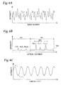
- spectral data is acquired from the spectroscope.
- the data at this time is diagrammatically illustrated in Fig. 6A .
- a step of S3 filtering is applied to the result of Fourier transform of the spectral data.
- the result of the Fourier transform becomes as illustrated in Fig. 6B , in which peaks of the optical distances appear at the positions of N 0 L 0 , N m1 L 1 , and N m2 L 2 . respectively. These optical distances correspond to the optical distances of the sample surface 205, the first interface 206 and the second interface 207, respectively, from the reference mirror 501.
- peaks also appear at N 1 D 1 , N 2 D 2 and N 12 D 12 , respectively, due to the interference of the multilayer structure itself, similar to the first embodiment.
- the reference mirror 501 it is preferable to set the reference mirror 501 in such a manner that the optical distance N 0 L 0 between this mirror 501 and the sample surface 205 be longer than the thickness N 12 D 12 of the entire multilayer structure. As a result, it is possible to separate a first region 601, in which the interference components of the sample itself appear, and a second region 602, in which the interference components of the sample and the reference mirror appear, from each other.
- the optical distance of the thus selected peak is calculated by a technique similar to that in the above-mentioned first embodiment.
- a result as illustrated in Fig. 6C is obtained by performing inverse Fourier transform on the selected peak.
- a step of S6 (corresponding to a seventh step of the present invention) an order of interference m is calculated from the above-mentioned interference condition expression 1 by specifying a wave number from the result of Fig. 6C .
- the order of interference m thus obtained is rounded off to an integer, and the optical distance is then calculated by substituting the integer in the interference condition expression.
- the spatial distance of each layer is obtained by subtracting an optical distance (N mi L i ) to an interface thereof at a side near the reference mirror from an optical distance (N mi+1 L i+1 ) to an interface thereof at a side far from the reference mirror, and by dividing it by a refractive index (N i+1 ) between both the interfaces.
- a tomographic image of the spatial distances based on Fig. 5 can be obtained.
- a conventional tomographic image is a tomographic image of the optical distances.
- a third embodiment of the present invention reference will be made to an optical system in an ophthalmic optical coherence apparatus to which the present invention is applied, while using Fig. 7 .
- the system has a basic construction of the type using the reference mirror of the second embodiment.
- Fig. 7 illustrates constructing a Mach-Zehnder interference system as a whole.
- the light emitted from a light source 701 is divided into reference light 705 and measurement light 706 by means of a beam splitter 703-1.
- the measurement light 706, after being returned, through reflection or scattering, as return light 708 by an eye 707 which is an object to be observed, is combined with the reference light 705 by means of a beam splitter 703-2 to enter a spectroscope 721.
- the light source 701 is an SLD (Super Luminescent Diode) that is a typical low coherent light source.
- the light source 701 has a wavelength of 830 nm, and a bandwidth of 50 nm.
- the bandwidth is an important parameter because it influences the resolution in the direction of an optical axis of a tomographic image to be obtained.
- the SLD is selected here for the light source, any kind of light source can be used which need only be able to emit low coherent light, and an ASE (Amplified Spontaneous Emission) or the like can be used.
- ASE Ampliclified Spontaneous Emission
- near infrared light is suitable for the wavelength to be used.
- the wavelength be as short as possible because it influences the resolution in the horizontal direction of a tomographic image to be obtained.
- a wavelength of 830 nm is used.
- other wavelengths can be selected depending upon a measurement portion of an object to be observed.
- the light emitted from the light source 701 is guided to a lens 711-1 through a single-mode fiber 710-1.
- reference numerals 715-1 and 715-2 denote dispersion compensation glasses.
- the dispersion compensation glass 715-1 compensates for dispersion of the measurement light 706 with respect to the reference light 705 when the measurement light 706 makes a round trip to the eye 707. In other words, it is desirable that the length L1 of the dispersion compensation glass 715-1 be equal to twice the depth of a general eye.
- the length L1 is set to 46 mm which is twice 23 mm which is assumed to be the diameter of an average eyeball of Japanese.
- an electric stage 717 is movable in a direction indicated by an arrow, so that it can adjust and control the optical path length of the reference light 705.
- the dispersion compensation glass 715-2 serves for the purpose of compensating for the dispersion of lenses 720-1 and 720-2 used to scan the eye 707.
- the measurement light 706 divided by the beam splitter 703-1 passes through a dispersion compensation glass 715-3, and is reflected by a beam splitter 703-3. Then, the measurement light 706 is incident on a mirror of an XY scanner 719.
- the XY scanner 719 raster-scans a retina 723 in a direction perpendicular to the optical axis of the measurement light 706.
- the center of the measurement light 706 is adjusted so as to coincide with the center of rotation of the mirror of the XY scanner 719.
- the lenses 720-1 and 720-2 together constitute an optical system for scanning the retina 723, and have a role to cause the measurement light 706 to scan the retina 723 with a location in the vicinity of a cornea 722 being placed as a fulcrum.
- the focal distances of the lenses 720-1 and 720-2 are 50 mm and 50 mm, respectively.
- the return light 708 is divided into return light 708-1 and return light 708-2 by means of the beam splitter 703-3, so that the one return light 708-1 is guided to the spectroscope 721, and the other return light 708-2 passes through the beam splitter 703-1 to be guided to a detector 724.
- An output signal of the detector 724 is electrically taken into a computer 725, similar to a interference signal, so that the intensity of the return light 708-2 can be recorded and displayed.
- the signal obtained by the detector 724 is an intensity signal of the return light 708-2 due to the reflection or scattering on the retina 723, and it does not have any depth resolution.
- an APD Avalanche Photo Diode
- the spatial distance of the entire retina is 560 ⁇ m, and is composed of seven layers, and the spatial distance of each layer is 80 ⁇ m.
- the refractive index of each layer is 1.5 (although no reflection will occur on each interface between adjacent layers unless the refractive indexes of the layers are different from each other, all the refractive indexes are herein set to the same value for simplifying the calculation of numerical values).
- the optical distance of each layer is 120 ⁇ m
- the optical distance of the entire retina is 840 ⁇ m.
- a minimum distance nd min that can be measured is 6.9 ⁇ m.
- N 1, 024
- a maximum distance nd max that can be measured is 3 mm (optical distance). If the interference spectrum is subjected to discrete Fourier transform, peaks stand out in the vicinity of 87, 104, 122, 139, 157, 174, 191, and 209 pixels because of 6.9 ⁇ m per pixel. These peaks are apart from one another, so they can be separated from one another.
- the optical distance is 1,440 ⁇ m, i.e., the longest
- the resolution of the spectroscope is 0.049 nm.
- m 4,000
- the measuring precision will be theoretically about 100 nm, though the condition changes depending upon the wavelength to be calculated. Since the measuring precision according to the discrete Fourier transform is 6.9 ⁇ m, it can be said that the measuring precision is improved to a significant extent.
- a tomographic image measuring method includes a first step of calculating information corresponding to an optical distance of each layer thickness from a wave-number spectrum, a second step of separating and extracting information of each layer from the information corresponding to the optical distance of each layer thickness, a third step of reconverting information of each layer into a wave-number spectrum, respectively, a fourth step of obtaining a interference wave number from the result of the third step, a fifth step of calculating an order of interference from the interference wave number and the optical distance of each layer; and a sixth step of calculating the optical distance of each layer by making use of the fact that the order of interference is an integer.
Landscapes
- Health & Medical Sciences (AREA)
- Physics & Mathematics (AREA)
- Life Sciences & Earth Sciences (AREA)
- General Physics & Mathematics (AREA)
- General Health & Medical Sciences (AREA)
- Surgery (AREA)
- Ophthalmology & Optometry (AREA)
- Heart & Thoracic Surgery (AREA)
- Medical Informatics (AREA)
- Molecular Biology (AREA)
- Engineering & Computer Science (AREA)
- Animal Behavior & Ethology (AREA)
- Biomedical Technology (AREA)
- Public Health (AREA)
- Veterinary Medicine (AREA)
- Nuclear Medicine, Radiotherapy & Molecular Imaging (AREA)
- Radiology & Medical Imaging (AREA)
- Biophysics (AREA)
- Length Measuring Devices By Optical Means (AREA)
- Investigating Or Analysing Materials By Optical Means (AREA)
- Instruments For Measurement Of Length By Optical Means (AREA)
Applications Claiming Priority (1)
| Application Number | Priority Date | Filing Date | Title |
|---|---|---|---|
| JP2008179311A JP5473265B2 (ja) | 2008-07-09 | 2008-07-09 | 多層構造計測方法および多層構造計測装置 |
Publications (1)
| Publication Number | Publication Date |
|---|---|
| EP2144034A1 true EP2144034A1 (fr) | 2010-01-13 |
Family
ID=41066405
Family Applications (1)
| Application Number | Title | Priority Date | Filing Date |
|---|---|---|---|
| EP09163477A Withdrawn EP2144034A1 (fr) | 2008-07-09 | 2009-06-23 | Procédé de mesure de structure multicouches et appareil de mesure de structure multicouches |
Country Status (4)
| Country | Link |
|---|---|
| US (1) | US20100007894A1 (fr) |
| EP (1) | EP2144034A1 (fr) |
| JP (1) | JP5473265B2 (fr) |
| CN (1) | CN101625319B (fr) |
Cited By (3)
| Publication number | Priority date | Publication date | Assignee | Title |
|---|---|---|---|---|
| GB2478590A (en) * | 2010-03-12 | 2011-09-14 | Precitec Optronik Gmbh | Apparatus and method for monitoring a thickness of a silicon wafer |
| TWI457536B (zh) * | 2011-03-03 | 2014-10-21 | Dainippon Screen Mfg | 膜形狀取得裝置及膜形狀取得方法 |
| ITBO20130403A1 (it) * | 2013-07-26 | 2015-01-27 | Marposs Spa | Metodo e apparecchiatura per il controllo ottico mediante interferometria dello spessore di un oggetto in lavorazione |
Families Citing this family (58)
| Publication number | Priority date | Publication date | Assignee | Title |
|---|---|---|---|---|
| JP5117787B2 (ja) * | 2007-08-13 | 2013-01-16 | 株式会社トプコン | 光画像計測装置 |
| JP5483873B2 (ja) * | 2008-12-26 | 2014-05-07 | キヤノン株式会社 | 光断層撮像装置、および光断層撮像方法 |
| JP5602363B2 (ja) * | 2008-12-26 | 2014-10-08 | キヤノン株式会社 | 光干渉断層撮像装置 |
| JP5570125B2 (ja) | 2009-01-22 | 2014-08-13 | キヤノン株式会社 | 光断層撮像装置 |
| JP5279524B2 (ja) * | 2009-01-22 | 2013-09-04 | キヤノン株式会社 | 光断層撮像装置、光断層撮像方法 |
| JP5558735B2 (ja) * | 2009-04-13 | 2014-07-23 | キヤノン株式会社 | 光断層撮像装置及びその制御方法 |
| JP5597012B2 (ja) * | 2010-03-31 | 2014-10-01 | キヤノン株式会社 | 断層画像撮像装置および断層画像撮像方法 |
| JP2012021856A (ja) * | 2010-07-14 | 2012-02-02 | Keyence Corp | 干渉膜厚計 |
| WO2012123947A2 (fr) * | 2011-03-14 | 2012-09-20 | G & D Innovative Analysis, Ltd. | Procédé et appareil pour analyse morphologique |
| GB2489722B (en) | 2011-04-06 | 2017-01-18 | Precitec Optronik Gmbh | Apparatus and method for determining a depth of a region having a high aspect ratio that protrudes into a surface of a semiconductor wafer |
| DE102011051146B3 (de) | 2011-06-17 | 2012-10-04 | Precitec Optronik Gmbh | Prüfverfahren zum Prüfen einer Verbindungsschicht zwischen waferförmigen Proben |
| US8917398B2 (en) | 2011-08-28 | 2014-12-23 | G & D Innovative Analysis Ltd. | Method and apparatus for supervision of optical material production |
| JP5942494B2 (ja) * | 2012-03-12 | 2016-06-29 | コニカミノルタ株式会社 | 厚さ測定装置及び厚さ測定方法 |
| FR2988478B1 (fr) * | 2012-03-20 | 2014-04-04 | European Aeronautic Defence & Space Co Eads France | Procede et dispositif de controle non destructif de la sante matiere notamment dans les conges d'une piece composite |
| FR2994734B1 (fr) * | 2012-08-21 | 2017-08-25 | Fogale Nanotech | Dispositif et procede pour faire des mesures dimensionnelles sur des objets multi-couches tels que des wafers. |
| DE102012111008B4 (de) | 2012-11-15 | 2014-05-22 | Precitec Optronik Gmbh | Optisches Messverfahren und optische Messvorrichtung zum Erfassen einer Oberflächentopographie |
| JP6057210B2 (ja) | 2012-12-13 | 2017-01-11 | 株式会社トプコン | 光学特性計測装置および光学特性計測方法 |
| TWI638131B (zh) | 2013-06-17 | 2018-10-11 | 普雷茨特光電有限公司 | 用於獲取距離差之光學量測裝置及光學量測方法 |
| JP6180909B2 (ja) * | 2013-12-06 | 2017-08-16 | 東京エレクトロン株式会社 | 距離を求める方法、静電チャックを除電する方法、及び、処理装置 |
| JP6435106B2 (ja) * | 2014-03-19 | 2018-12-05 | 株式会社ティーワイテクノ | 塗装膜解析方法 |
| US10255661B2 (en) | 2014-06-11 | 2019-04-09 | Canon Kabushiki Kaisha | Object information acquiring apparatus and image processing method |
| CN107110642B (zh) * | 2014-12-22 | 2019-12-17 | 庞巴迪公司 | 用于在线视觉检查的参考系统 |
| AU2015374335B2 (en) | 2014-12-23 | 2018-03-29 | Apple Inc. | Optical inspection system and method including accounting for variations of optical path length within a sample |
| CN105147238B (zh) * | 2015-06-19 | 2017-03-08 | 东北大学 | 一种眼睛多界面间距测量方法及装置 |
| CN108449957B (zh) | 2015-09-01 | 2021-03-09 | 苹果公司 | 用于非接触式感测物质的基准开关架构 |
| FR3045813B1 (fr) * | 2015-12-22 | 2020-05-01 | Unity Semiconductor | Dispositif et procede de mesure de hauteur en presence de couches minces |
| CN109073460B (zh) | 2016-04-21 | 2022-08-23 | 苹果公司 | 用于参考切换的光学系统 |
| US10234265B2 (en) | 2016-12-12 | 2019-03-19 | Precitec Optronik Gmbh | Distance measuring device and method for measuring distances |
| JP6776115B2 (ja) | 2016-12-22 | 2020-10-28 | キヤノン株式会社 | 処理装置および処理方法 |
| JP6333351B1 (ja) * | 2016-12-27 | 2018-05-30 | Ntn株式会社 | 測定装置、塗布装置、および膜厚測定方法 |
| US10480925B2 (en) * | 2017-01-19 | 2019-11-19 | Applejack 199 L.P. | Inspecting a slab of material |
| JP6731868B2 (ja) | 2017-02-17 | 2020-07-29 | 株式会社Screenホールディングス | 撮像方法および撮像装置 |
| US10113860B1 (en) * | 2017-04-12 | 2018-10-30 | Applejack 199, L.P. | Inspecting a multilayer sample |
| US10890434B2 (en) | 2017-04-12 | 2021-01-12 | Applejack 199 L.P. | Inspecting a multilayer sample |
| EP3688446A2 (fr) | 2017-09-29 | 2020-08-05 | Apple Inc. | Architectures d'échantillonnage optique de chemin de résolution |
| DE102017126310A1 (de) | 2017-11-09 | 2019-05-09 | Precitec Optronik Gmbh | Abstandsmessvorrichtung |
| CN110118533B (zh) * | 2018-02-05 | 2021-08-03 | 上海微电子装备(集团)股份有限公司 | 一种三维检测方法及检测装置 |
| CN114545550B (zh) | 2018-02-13 | 2024-05-28 | 苹果公司 | 具有集成边缘外耦合器的集成光子装置 |
| CN109164588A (zh) * | 2018-08-30 | 2019-01-08 | 天津大学 | 一种实现透过散射介质聚焦的偏振相移相位共轭方法 |
| DE102018130901A1 (de) | 2018-12-04 | 2020-06-04 | Precitec Optronik Gmbh | Optische Messeinrichtung |
| CN109632711B (zh) * | 2019-01-10 | 2021-10-01 | 山东拓步教育科技有限公司 | 一种ps小球层数检测装置 |
| CN109884588B (zh) * | 2019-01-16 | 2020-11-17 | 北京大学 | 一种脉冲序列的距离度量方法及系统 |
| CN112748111B (zh) * | 2019-10-31 | 2022-09-27 | 上海微电子装备(集团)股份有限公司 | 三维检测装置及三维检测方法 |
| CN110986890B (zh) * | 2019-11-26 | 2022-03-25 | 北京经纬恒润科技股份有限公司 | 高度检测方法及装置 |
| JP7507414B2 (ja) * | 2020-05-26 | 2024-06-28 | パナソニックIpマネジメント株式会社 | シート作成装置、シート作成方法、及び複層シートの厚さを算出する装置 |
| EP4168734B1 (fr) | 2020-06-19 | 2025-09-24 | Precitec Optronik GmbH | Appareil de mesure confocal chromatique |
| EP4176304A1 (fr) | 2020-09-09 | 2023-05-10 | Apple Inc. | Système optique d'atténuation de bruit |
| US20240044637A1 (en) * | 2020-11-11 | 2024-02-08 | Nippon Telegraph And Telephone Corporation | Film Thickness Measurement Device and Method |
| KR102494082B1 (ko) * | 2021-01-28 | 2023-01-31 | 서울대학교산학협력단 | 간섭과 파수 고주파 변조를 이용한 박막 두께와 형상을 측정하는 장치 및 그 장치를 이용한 박막 두께와 형상 측정 방법 |
| CN113189019B (zh) * | 2021-04-21 | 2023-03-07 | 山西大学 | 基于光学频率梳的多层结构材料特性测量装置和方法 |
| US20220371152A1 (en) * | 2021-05-20 | 2022-11-24 | Applied Materials, Inc. | Fourier filtering of spectral data for measuring layer thickness during substrate processing |
| CN116148007B (zh) * | 2022-03-08 | 2025-04-18 | 上海超导科技股份有限公司 | 超导带材微观结构置样方法 |
| CN114894712B (zh) * | 2022-03-25 | 2023-08-25 | 业成科技(成都)有限公司 | 光学量测设备及其校正方法 |
| CN115035036B (zh) * | 2022-05-09 | 2025-03-11 | 北京转转精神科技有限责任公司 | 一种屏幕检测方法以及装置 |
| US12578076B2 (en) | 2023-06-05 | 2026-03-17 | Hamamatsu Photonics K.K. | Dual-output laser-driven light source |
| US12085387B1 (en) * | 2023-09-23 | 2024-09-10 | Hamamatsu Photonics K.K. | Optical coherence tomography system for subsurface inspection |
| CN120876579B (zh) * | 2025-09-26 | 2025-11-28 | 中国科学院长春光学精密机械与物理研究所 | 用于光学元件厚度检测的sd-oct系统及其检测方法 |
| CN121631993B (zh) * | 2026-02-05 | 2026-04-03 | 厦门理工学院 | 一种检测透明平板间隙的光学相干断层成像方法和系统 |
Citations (2)
| Publication number | Priority date | Publication date | Assignee | Title |
|---|---|---|---|---|
| US20040080761A1 (en) | 2002-10-28 | 2004-04-29 | Tevet Process Control Technologies Ltd. | Method and apparatus for thickness decomposition of complicated layer structures |
| WO2006125131A2 (fr) | 2005-05-19 | 2006-11-23 | Zygo Corporation | Procede et systeme d'analyse de signaux d'interferometrie a faible coherence pour des informations concernant des structures a minces films |
Family Cites Families (12)
| Publication number | Priority date | Publication date | Assignee | Title |
|---|---|---|---|---|
| JP2539283B2 (ja) * | 1990-07-09 | 1996-10-02 | 日本分光工業株式会社 | 膜厚測定方法 |
| JPH074922A (ja) * | 1993-06-21 | 1995-01-10 | Jasco Corp | 半導体多層薄膜膜厚測定装置およびその測定方法 |
| JPH10311708A (ja) * | 1997-05-13 | 1998-11-24 | Tokyo Seimitsu Co Ltd | 干渉式膜厚計 |
| DE19814057B4 (de) * | 1998-03-30 | 2009-01-02 | Carl Zeiss Meditec Ag | Anordnung zur optischen Kohärenztomographie und Kohärenztopographie |
| JP4242767B2 (ja) * | 2001-09-21 | 2009-03-25 | ケイマック | 2次元型検出器を用いた薄膜特性測定装置及びその測定方法 |
| JP2003240515A (ja) * | 2002-02-15 | 2003-08-27 | Toray Ind Inc | 膜厚測定方法およびシートの製造方法 |
| JP2005160694A (ja) * | 2003-12-02 | 2005-06-23 | Microtomography Kk | 多重波面光コヒーレンスによる眼球内距離測定装置 |
| US7177030B2 (en) * | 2004-04-22 | 2007-02-13 | Technion Research And Development Foundation Ltd. | Determination of thin film topography |
| US7301644B2 (en) * | 2004-12-02 | 2007-11-27 | University Of Miami | Enhanced optical coherence tomography for anatomical mapping |
| WO2006078802A1 (fr) * | 2005-01-21 | 2006-07-27 | Massachusetts Institute Of Technology | Procedes et appareil pour le balayage de la tomographie de coherence optique |
| JP2007003456A (ja) * | 2005-06-27 | 2007-01-11 | Sony Disc & Digital Solutions Inc | 膜厚測定方法、膜厚測定装置 |
| CN100507513C (zh) * | 2006-09-27 | 2009-07-01 | 中国科学院上海光学精密机械研究所 | 介质薄膜群延迟的测量方法 |
-
2008
- 2008-07-09 JP JP2008179311A patent/JP5473265B2/ja not_active Expired - Fee Related
-
2009
- 2009-06-18 US US12/487,026 patent/US20100007894A1/en not_active Abandoned
- 2009-06-23 EP EP09163477A patent/EP2144034A1/fr not_active Withdrawn
- 2009-07-09 CN CN2009101402379A patent/CN101625319B/zh not_active Expired - Fee Related
Patent Citations (2)
| Publication number | Priority date | Publication date | Assignee | Title |
|---|---|---|---|---|
| US20040080761A1 (en) | 2002-10-28 | 2004-04-29 | Tevet Process Control Technologies Ltd. | Method and apparatus for thickness decomposition of complicated layer structures |
| WO2006125131A2 (fr) | 2005-05-19 | 2006-11-23 | Zygo Corporation | Procede et systeme d'analyse de signaux d'interferometrie a faible coherence pour des informations concernant des structures a minces films |
Non-Patent Citations (3)
| Title |
|---|
| D. KIM ET AL., OPTICS LETTERS, vol. 27, 2002, pages 1893 - 1895 |
| KIM D ET AL: "Measurement of the thickness profile of a transparent thin film deposited upon a pattern structure with an acousto-optic tunable filter", 1 November 2002, OPTICS LETTERS 20021101 OPTICAL SOCIETY OF AMERICA US, VOL. 27, NR. 21, PAGE(S) 1893 - 1895, XP002547752 * |
| SEMI, 3081 ZANKER ROAD, SAN JOSE, CA 95134, USA, November 2003 (2003-11-01), XP040454207 * |
Cited By (7)
| Publication number | Priority date | Publication date | Assignee | Title |
|---|---|---|---|---|
| GB2478590A (en) * | 2010-03-12 | 2011-09-14 | Precitec Optronik Gmbh | Apparatus and method for monitoring a thickness of a silicon wafer |
| US8699038B2 (en) | 2010-03-12 | 2014-04-15 | Precitec Optronik Gmbh | Apparatus and method for monitoring a thickness of a silicon wafer with a highly doped layer |
| US9230817B2 (en) | 2010-03-12 | 2016-01-05 | Precitec Optronik Gmbh | Apparatus and method for monitoring a thickness of a silicon wafer with a highly doped layer |
| TWI457536B (zh) * | 2011-03-03 | 2014-10-21 | Dainippon Screen Mfg | 膜形狀取得裝置及膜形狀取得方法 |
| ITBO20130403A1 (it) * | 2013-07-26 | 2015-01-27 | Marposs Spa | Metodo e apparecchiatura per il controllo ottico mediante interferometria dello spessore di un oggetto in lavorazione |
| WO2015011243A1 (fr) * | 2013-07-26 | 2015-01-29 | Marposs Societa' Per Azioni | Procédé et appareil de vérification optique par interférométrie de l'épaisseur d'un objet usiné |
| US9879978B2 (en) | 2013-07-26 | 2018-01-30 | Marposs Societa' Per Azioni | Method and apparatus for optically checking by interferometry the thickness of an object being machined |
Also Published As
| Publication number | Publication date |
|---|---|
| JP2010019636A (ja) | 2010-01-28 |
| CN101625319B (zh) | 2011-06-29 |
| US20100007894A1 (en) | 2010-01-14 |
| CN101625319A (zh) | 2010-01-13 |
| JP5473265B2 (ja) | 2014-04-16 |
Similar Documents
| Publication | Publication Date | Title |
|---|---|---|
| EP2144034A1 (fr) | Procédé de mesure de structure multicouches et appareil de mesure de structure multicouches | |
| KR102558264B1 (ko) | 다층 스택의 계측 | |
| US8836952B2 (en) | Optical coherence tomographic imaging method and optical coherence tomographic imaging apparatus | |
| US8565499B2 (en) | Methods, systems, and computer readable media for synthetic wavelength-based phase unwrapping in optical coherence tomography and spectral domain phase microscopy | |
| KR101384005B1 (ko) | 광간섭 단층법을 사용하는 촬상 장치 및 촬상 방법, 및 컴퓨터 판독가능 저장 매체 | |
| EP1887926B1 (fr) | Systeme et procede qui utilisent des techniques d'interferometrie d'heterodyne a codage spectral pour l'imagerie | |
| US9310187B2 (en) | Image capturing apparatus, image capturing method, and storage medium | |
| CN114894308B (zh) | 一种基于低相干干涉的光谱仪标定方法与系统 | |
| CN109211415A (zh) | 一种基于光源光谱特征波长的波长标定方法 | |
| KR101919957B1 (ko) | 순간적 시간 영역 광 간섭 단층 촬영 | |
| Ruis et al. | Decreasing the size of a spectral domain optical coherence tomography system with cascaded arrayed waveguide gratings in a photonic integrated circuit | |
| Oldenburg et al. | Plasmon-resonant gold nanorods provide spectroscopic OCT contrast in excised human breast tumors | |
| Yurdakul et al. | Line-field coherent sensing with LED illumination | |
| Francis et al. | Low-coherence and broadband confocal refractometry: reducing the measurement time | |
| Verrier et al. | Influence of interfaces reflectivity for central thickness measurement of a contact lens by low coherence interferometry |
Legal Events
| Date | Code | Title | Description |
|---|---|---|---|
| PUAI | Public reference made under article 153(3) epc to a published international application that has entered the european phase |
Free format text: ORIGINAL CODE: 0009012 |
|
| AK | Designated contracting states |
Kind code of ref document: A1 Designated state(s): AT BE BG CH CY CZ DE DK EE ES FI FR GB GR HR HU IE IS IT LI LT LU LV MC MK MT NL NO PL PT RO SE SI SK TR |
|
| 17P | Request for examination filed |
Effective date: 20100713 |
|
| 17Q | First examination report despatched |
Effective date: 20140813 |
|
| STAA | Information on the status of an ep patent application or granted ep patent |
Free format text: STATUS: THE APPLICATION HAS BEEN WITHDRAWN |
|
| 18W | Application withdrawn |
Effective date: 20150305 |