EP2144265A1 - Commutateur MEMS RF - Google Patents
Commutateur MEMS RF Download PDFInfo
- Publication number
- EP2144265A1 EP2144265A1 EP09158547A EP09158547A EP2144265A1 EP 2144265 A1 EP2144265 A1 EP 2144265A1 EP 09158547 A EP09158547 A EP 09158547A EP 09158547 A EP09158547 A EP 09158547A EP 2144265 A1 EP2144265 A1 EP 2144265A1
- Authority
- EP
- European Patent Office
- Prior art keywords
- contact
- mems switch
- leg
- signal line
- metal contact
- Prior art date
- Legal status (The legal status is an assumption and is not a legal conclusion. Google has not performed a legal analysis and makes no representation as to the accuracy of the status listed.)
- Withdrawn
Links
- 239000000463 material Substances 0.000 claims abstract description 25
- 238000002955 isolation Methods 0.000 claims abstract description 13
- 229910052751 metal Inorganic materials 0.000 claims description 35
- 239000002184 metal Substances 0.000 claims description 35
- 239000000758 substrate Substances 0.000 claims description 18
- 238000004519 manufacturing process Methods 0.000 description 18
- 229910021420 polycrystalline silicon Inorganic materials 0.000 description 7
- 229920005591 polysilicon Polymers 0.000 description 7
- VYPSYNLAJGMNEJ-UHFFFAOYSA-N Silicium dioxide Chemical compound O=[Si]=O VYPSYNLAJGMNEJ-UHFFFAOYSA-N 0.000 description 4
- 238000000151 deposition Methods 0.000 description 4
- 238000000034 method Methods 0.000 description 4
- 230000004913 activation Effects 0.000 description 2
- 230000005540 biological transmission Effects 0.000 description 2
- 150000004649 carbonic acid derivatives Chemical class 0.000 description 2
- 239000000919 ceramic Substances 0.000 description 2
- 239000000356 contaminant Substances 0.000 description 2
- 239000010432 diamond Substances 0.000 description 2
- 239000011521 glass Substances 0.000 description 2
- 150000004767 nitrides Chemical class 0.000 description 2
- 238000004806 packaging method and process Methods 0.000 description 2
- 239000002245 particle Substances 0.000 description 2
- 238000000059 patterning Methods 0.000 description 2
- BASFCYQUMIYNBI-UHFFFAOYSA-N platinum Chemical compound [Pt] BASFCYQUMIYNBI-UHFFFAOYSA-N 0.000 description 2
- 235000012239 silicon dioxide Nutrition 0.000 description 2
- 239000000377 silicon dioxide Substances 0.000 description 2
- 239000007787 solid Substances 0.000 description 2
- 241000408659 Darpa Species 0.000 description 1
- 229910052581 Si3N4 Inorganic materials 0.000 description 1
- XUIMIQQOPSSXEZ-UHFFFAOYSA-N Silicon Chemical compound [Si] XUIMIQQOPSSXEZ-UHFFFAOYSA-N 0.000 description 1
- 230000009286 beneficial effect Effects 0.000 description 1
- 230000000694 effects Effects 0.000 description 1
- 238000005530 etching Methods 0.000 description 1
- 239000012535 impurity Substances 0.000 description 1
- 238000007373 indentation Methods 0.000 description 1
- 230000007935 neutral effect Effects 0.000 description 1
- 238000000206 photolithography Methods 0.000 description 1
- 229910052697 platinum Inorganic materials 0.000 description 1
- 229910052710 silicon Inorganic materials 0.000 description 1
- 239000010703 silicon Substances 0.000 description 1
- HQVNEWCFYHHQES-UHFFFAOYSA-N silicon nitride Chemical compound N12[Si]34N5[Si]62N3[Si]51N64 HQVNEWCFYHHQES-UHFFFAOYSA-N 0.000 description 1
- 239000000126 substance Substances 0.000 description 1
Images


Classifications
-
- H—ELECTRICITY
- H01—ELECTRIC ELEMENTS
- H01H—ELECTRIC SWITCHES; RELAYS; SELECTORS; EMERGENCY PROTECTIVE DEVICES
- H01H59/00—Electrostatic relays; Electro-adhesion relays
- H01H59/0009—Electrostatic relays; Electro-adhesion relays making use of micromechanics
-
- H—ELECTRICITY
- H01—ELECTRIC ELEMENTS
- H01H—ELECTRIC SWITCHES; RELAYS; SELECTORS; EMERGENCY PROTECTIVE DEVICES
- H01H1/00—Contacts
- H01H1/0036—Switches making use of microelectromechanical systems [MEMS]
- H01H2001/0084—Switches making use of microelectromechanical systems [MEMS] with perpendicular movement of the movable contact relative to the substrate
Definitions
- the present invention relates generally to a radio frequency ("RF") MEMS circuit and method of fabricating an RF MEMS circuit. More particularly, the invention relates to a circuit and method of fabricating an RF MEMS circuit having a large restoring force and a small contact area.
- RF radio frequency
- RF MEMS switches may be used for switchable signal routing and time-delay phase-shifter networks, among other applications.
- An RF MEMS switch may be electrically configured in series or in parallel with a radio frequency transmission line. The device may be designed to switch the transmission line on or off when the RF MEMS device is activated.
- RF MEMS switches may have a beam having a contact.
- the beam may have one leg or several legs supporting the beam.
- a supporting force from the beam legs and the tendency of the beam to return to its original position before it was deflected may provide a restoring spring force to restore the beam to its neutral position.
- RF MEMS switches may also have RF contacts located near a signal line.
- an RF MEMS switch When an RF MEMS switch is activated by applying an actuation voltage between the beam and the RF grounds, an electrostatic force may be created between the beam and the RF grounds. The electrostatic force may pull the beam toward the RF grounds, causing the contact on the beam to come into contact with a contact on the signal line.
- the signal line may be switched on or off by applying an actuation voltage to an RF MEMS switch.
- the signal line contact and the contact on the beam have good contact force between them. This may be accomplished by providing a large electrostatic force to pull the beam toward the signal line contact and to provide a force to hold the beam contact against the signal line contact.
- the nature of the contact or impurities or foreign particles between the contacts may cause the beam contact to stick to the signal line contact, a problem known as stiction. Stiction may negatively affect the reliability of the switching device. If the beam contact sticks to the signal line contact, and the restoring spring force is insufficient to restore the beam to its unactivated position, the switch will be stuck in an activated position even when the activation voltage is removed.
- One way to counteract problems with stiction is to provide a large restoring force from the beam and the beam legs.
- the beam may cause interference with the RF signal. Therefore, in order to minimize problems with RF interference it may be problematic to implement a large beam and beam legs.
- the RF MEMS switch has a large beam and beam legs that may provide a large restoring force to pull the switch open when an activation voltage is removed.
- the beam and beam legs may be composed of a material having a high resistivity and a large Young's modulus, such as polysilicon, some crystalline and polycrystalline carbonates, nitrides, and diamonds ( e . g ., SiC, AlN).
- the high resistivity of the beam material may provide minimal interference with the RF signal passing through the switch. Because of the high resistivity of the beam material, the beam and beam legs may be large and in close proximity to the RF signal lines and may still provide minimal interference with the RF signals passing through the RF MEMS switch.
- the actuation voltage may be reduced to achieve a given electrostatic force.
- a large electrostatic force may also enable the distance between the beam and the substrate to be increased, which may provide improved electrical isolation.
- placing the contact(s) near the center of the beam may also increase the contact force achieved for a given beam surface area.
- Stiction between the beam contact and the signal line contact may occur due to contaminants or other particles in contact with the beam contact or signal line contact.
- a metal contact may be provided on the beam. The metal contact may have a small raised contact area. A small raised contact area may minimize stiction by reducing the area of contact between the beam contact and the signal line contact. Because the raised contact area may be small relative to the beam, the electrostatic force and restoring force may be large, while stiction may be minimized.
- an RF MEMS switch having a beam and beam legs composed of a material having a high resistivity and a large Young's modulus may reduce switch reliability problems due to stiction, while maintaining a large contact and restoring force to provide good contact between the beam contact and the signal line contact.
- An RF MEMS switch and a method of fabricating an RF MEMS switch that may provide improved reliability and improved resistance to stiction is described.
- An RF MEMS switch may have a signal line with a signal line contact area and a beam supported by at least one beam leg having a beam contact area.
- an actuation voltage When an actuation voltage is applied between the beam and actuation contacts located on the substrate, an electrostatic force may pull the beam downward.
- the beam contact may make electrical contact with the signal line contact.
- a beam and beam legs may be composed of a material having a high resistivity.
- a material having a resistivity of at least at least 1000 ⁇ -cm would provide desirably low levels of RF interference.
- a high resistivity may provide reduced interference with RF signals passing through or disconnected by the RF MEMS switch. Because the interference with RF signals may be reduced, the size of the beam and beam legs may be increased without providing unacceptable levels of RF interference.
- a large beam and beam legs may provide a large restoring force to open the switch when the actuation voltage is removed.
- the beam legs may have a thickness equal to or greater than the thickness of the beam. For a beam and beam legs composed of high resistivity polysilicon, the thicknesses may be greater than 4.0 ⁇ m.
- Examples a high resistivity material which may be used to compose the beam and beam legs are polysilicon, some crystalline and polycrystalline carbonates, nitrides, and diamonds ( e . g ., SiC, A1N). These materials may also have a large Young's modulus, i . e . greater than 150GPa, which may provide a large restoring force to restore the beam when the RF MEMS switch is in an unactivated state.
- a large surface area of the beam may provide an increased electrostatic force for a given actuation voltage.
- a beam having a surface area of approximately 1-8x10 -8 m 2 may provide low actuation voltages of approximately 18-40V.
- beam legs having lengths of approximately 40-60 ⁇ m and a thickness of 4-8 ⁇ m may provide a restoring force of approximately 350-630 ⁇ N. Therefore, large electrostatic forces may be produced while maintaining low actuation voltages.
- the resistivity of the beam may cause the conductivity to be so low that the actuation voltage may not be sufficient to provide enough electrostatic force to pull down the beam.
- a thin layer of a highly conductive metal such as platinum, may be deposited on the top of the beam. This may increase the conductivity of the beam as a whole and may allow accurate beam response to the actuation voltage.
- the highly conductive metal may be any highly conductive metal known in the art. Methods of depositing metal layers are well known in the art and not described herein.
- a large electrical permittivity may provide an increased electrostatic force for a given actuation voltage for a polysilicon beam having a metal layer deposited on top of the beam.
- polysilicon may have a relative permittivity of approximately 11.9.
- a metal contact located on the beam may come into electrical contact with a signal line contact located on the RF MEMS switch.
- the metal contact on the beam may have a raised profile that forms a contact bumps or contact bumps.
- the contact bump may come into physical contact with the signal line when the switch is activated.
- the contact bumps may be approximately 0.2% - 1% of the beam surface area.
- the small contact area between the beam and the signal line contact and the large restoring force may reduce the possibility of failure due to stiction.
- the distance between the beam and the substrate may be increased because of the large electrostatic force.
- the beam may be located approximately 2 ⁇ m above the signal line contact.
- the increased distance between the beam and the signal line contact may provide improved electrical isolation when the switch is in an open state.
- the isolation of an open switch of the present invention may have isolation values of approximately 30 dB.
- an RF MEMS switch having a beam and beam legs composed of a material having a high resistivity and a large Young's modulus may reduce switch reliability problems due to stiction by applying a large restoring force, while maintaining a large contact force to provide good contact between the contact bump and the signal line contact.
- Fig 1a shows a top view of a base level of an RF MEMS switch 10.
- the RF MEMS switch 10 may have an actuation contact 1, a signal line contact 3, signal electrodes 5, and signal line 7.
- the signal line contact 3 may come into electrical contact with a contact on a beam, discussed further with respect to Fig. 1b .
- the RF MEMS switch 10 may achieve an "on" position when the beam contact electrically contacts the signal line contact 3, and an RF signal may pass through an electric path between the beam and the signal line 7.
- the signal electrodes 5 may be located on the signal line 7.
- the signal electrodes 5 may be contacted to receive the RF signal conducted by the signal line 7.
- An actuation voltage may be applied across actuation contacts 1.
- the actuation voltage may create a voltage differential between the beam and the actuation contacts 1, creating an electrostatic force between the actuation contact 1 and the beam, discussed further with respect to Fig. 1b .
- the amount of electrostatic force is proportional to the area of the beam and the actuation contacts, the electric permittivity of electrically insulating areas located between the beam and the actuation contacts 1, and the square of the actuation voltage applied, and is inversely proportional to the square of the vertical distance between the beam and the signal line contact 3. Therefore, a material having a large surface area may have a large electrostatic force for a given actuation voltage.
- Fig. 1b shows the RF MEMS switch 10 with the beam 9 and the beam legs 11.
- the RF MEMS switch 10 shown has four beam legs 11; however, other numbers of beam legs 11 may be used.
- the beam 9 may be supported by the beam legs 11. When the beam 9 is deflected by the electrostatic force created by the actuation voltage, the beam legs 11 may provide a restoring force to the beam 9 to return the beam 9 to its "off" position.
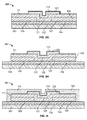
- Figs. 2a-2l are side views showing a method of manufacturing an RF MEMS switch 101.
- a substrate 103 is provided. Any substrate material known in the art may be used. Glass or ceramic substrates may have beneficial properties in that a glass or ceramic substrate 103 may cause less conductive loss through the substrate 103 than other known silicon substrates. Actuation electrodes are located on the substrate 103.
- An actuation electrode 102 may be deposited on the substrate 103. Methods of patterning and depositing actuation electrodes are well known in the art and are not described in detail herein.
- An isolation layer 104 may be deposited over the actuation electrode 102.
- the isolation layer may be silicon nitride, for example.
- a first metal contact 107 may be deposited on the substrate.
- the first metal layer 107 may be any metal known in the art that may be deposited on a substrate.
- the first metal contact 107 may be patterned to have the desired profile, for example, by using a photolithography and wet or dry etch. Methods of patterning and etching materials in the manufacture of integrated circuits are well known in the art and not described in detail herein.
- a first sacrificial layer 105 may be deposited.
- the first sacrificial layer 105 may be silicon dioxide, for example.
- the first sacrificial layer 105 and the first metal contact 107 may be planarized to have a flat profile.
- a second sacrificial layer 109 may be deposited and patterned.
- the second sacrificial layer 109 may be silicon dioxide, for example.
- the second sacrificial layer 109 may be patterned to have a gap that exposes the first metal contact 107.
- a third sacrificial layer 111 may be deposited.
- the indentation formed in the third sacrificial layer 111 due to the gap in the second sacrificial layer 109 may provide a space for a second metal contact 123 having a raised profile, as shown in Fig. 2f .
- the raised profile of the second metal contact 123 forms a contact bump 131.
- the small surface area of the contact bump 131 compared to the second metal contact 123 provides a small contact area between the first metal contact 107 and the second metal contact 123, resulting in the advantages discussed above.
- an isolation layer 113 may be deposited over the third sacrificial layer and the second metal contact 123.
- the isolation layer 113 may electrically and physically isolate the second metal contact 123 from the beam, discussed further with respect to Fig. 2i .
- the isolation layer 113 may be any dielectric substance known in the art that may insulate layers from electrical contract with each other.
- the first, second, and third sacrificial layers 105, 109, 111 and the isolation layer 113 may be patterned to provide areas 300 on the substrate for the beam legs, discussed further with respect to Fig. 2i .
- a layer of polysilicon may be deposited and patterned to form a beam horizontal portion 119 and beam vertical portion 115.
- the beam vertical portion 115 may be solid.
- a fourth sacrificial layer 117 may be deposited and patterned.
- a sacrificial removal channel 121 may also be deposited, to provide an area to apply the etch to remove the sacrificial layers 105, 109, 111, 117 when the package layer, discussed further with respect to Fig. 2k , may be deposited over the fourth sacrificial layer 117.
- the sacrificial removal channel 121 is shown in Fig. 2j as having a similar thickness at the fourth sacrificial layer 117; however the sacrificial removal channel 121 may be any thickness and may preferably be smaller than the fourth sacrificial layer 117.
- a package layer 127 is deposited over the fourth sacrificial layer 117.
- the package layer 127 may be any material used in packaging integrated circuits.
- the sacrificial layers 105, 109. 111, 117 may be removed with an etch.
- the gap 125 between the beam horizontal portion 119 and the first metal contact 107 may be filled with air or another gas, and may be a vacuum.
- the space remaining between the package 127 and the substrate 103 may be sealed after the sacrificial layers 105, 109, 111, 117 are removed, described further with respect to Fig. 2l .
- the package 127 may protect the RF MEMS switch 101 from unwanted contaminants, for example.
- the sacrificial removal channel 121 may be sealed by depositing a material 129 to seal the sacrificial removal channel 121.
- the material 129 may be the material used for the package layer 127, or, alternatively, may be any material known in the art used to package integrated circuits.
- the RF MEMS switch has a space between the first metal contact 107 and the contact bump 131.
- the beam horizontal portion 119 is drawn toward the substrate 103, placing the first metal contacts 107 and the contact bump 131 in electrical contact.
- the beam vertical portion 115 supports the beam horizontal portion 119 and provides a restoring force when the beam horizontal portion 119 is deflected.
- the thickness of the third sacrificial layers 111 may be designed to create a predetermined distance between the bottom surface of the contact bump 131 and the first metal contact 107.
- the total thicknesses of the second and third sacrificial layers 109, 111 may be determined to create a predetermined distance between the bottom surface of the beam horizontal portion 119 and the first metal contact 107. These distances may be designed to optimize the contact force between the contact bump 131 and the first metal layer 107 and the restoring force from the beam vertical portion 115.
- the beam horizontal portion 119 may have a cantilever configuration, supported on one side by at least one beam vertical portion 115.
- the RF MEMS switch 101 may be fabricated as described with respect to Figs. 2a-h .
- a layer of polysilicon may be deposited and patterned to form a beam horizontal portion 119 and at least one beam vertical portion 115.
- the beam vertical portion 115 may be solid. Alternatively, there may be multiple beam vertical portions 115 supporting the beam horizontal portion 119.
- a fourth sacrificial layer 117 may be deposited and patterned.
- a sacrificial removal channel 121 may be deposited.
- the sacrificial removal channel 121 is shown in Fig. 2j as having a similar thickness at the fourth sacrificial layer 117; however the sacrificial removal channel 121 may be any thickness and may preferably be smaller than the fourth sacrificial layer 117.
- a package layer 127 is deposited over the fourth sacrificial layer 117.
- the package layer 127 may be any material used in packaging integrated circuits.
- An etch may be applied across the sacrificial removal channel 121 to remove the sacrificial layers 105, 109. 111, 117.
- the gap 125 between the beam horizontal portion 119 and the first metal contact 107 may be filled with air or another gas, and may be a vacuum.
- the sacrificial removal channel 121 may be sealed by depositing a material 129 to fill the sacrificial removal channel 121.
- the material 129 may be the material used for the package layer 127, or, alternatively, may be any material known in the art used to package integrated circuits.
Landscapes
- Micromachines (AREA)
Applications Claiming Priority (1)
| Application Number | Priority Date | Filing Date | Title |
|---|---|---|---|
| US12/168,647 US20100001355A1 (en) | 2008-07-07 | 2008-07-07 | RF MEMS Switch |
Publications (1)
| Publication Number | Publication Date |
|---|---|
| EP2144265A1 true EP2144265A1 (fr) | 2010-01-13 |
Family
ID=41128162
Family Applications (1)
| Application Number | Title | Priority Date | Filing Date |
|---|---|---|---|
| EP09158547A Withdrawn EP2144265A1 (fr) | 2008-07-07 | 2009-04-22 | Commutateur MEMS RF |
Country Status (2)
| Country | Link |
|---|---|
| US (1) | US20100001355A1 (fr) |
| EP (1) | EP2144265A1 (fr) |
Cited By (2)
| Publication number | Priority date | Publication date | Assignee | Title |
|---|---|---|---|---|
| WO2012040092A1 (fr) * | 2010-09-21 | 2012-03-29 | Cavendish Kinetics, Inc | Électrode d'excursion haute et microstructure à réseau croisé |
| CN103917481A (zh) * | 2011-06-20 | 2014-07-09 | 国际商业机器公司 | 微机电系统(mems)以及相关的致动器凸块、制造方法和设计结构 |
Families Citing this family (8)
| Publication number | Priority date | Publication date | Assignee | Title |
|---|---|---|---|---|
| US7998775B2 (en) * | 2009-02-09 | 2011-08-16 | Taiwan Semiconductor Manufacturing Company, Ltd. | Silicon undercut prevention in sacrificial oxide release process and resulting MEMS structures |
| US8278748B2 (en) * | 2010-02-17 | 2012-10-02 | Maxim Integrated Products, Inc. | Wafer-level packaged device having self-assembled resilient leads |
| US8797127B2 (en) | 2010-11-22 | 2014-08-05 | Taiwan Semiconductor Manufacturing Company, Ltd. | MEMS switch with reduced dielectric charging effect |
| US9233832B2 (en) * | 2013-05-10 | 2016-01-12 | Globalfoundries Inc. | Micro-electro-mechanical system (MEMS) structures and design structures |
| CN103943419A (zh) * | 2014-04-15 | 2014-07-23 | 苏州锟恩电子科技有限公司 | 一种带有上悬梁的RFMEMs开关 |
| US20160009548A1 (en) * | 2014-04-17 | 2016-01-14 | Skyworks Solutions, Inc. | Microelectromechanical systems having contaminant control features |
| FR3051458B1 (fr) * | 2016-05-20 | 2020-09-04 | Univ Limoges | Commutateur variable microelectromecanique radiofrequence |
| WO2023082187A1 (fr) * | 2021-11-12 | 2023-05-19 | 京东方科技集团股份有限公司 | Déphaseur |
Citations (2)
| Publication number | Priority date | Publication date | Assignee | Title |
|---|---|---|---|---|
| EP1343189A2 (fr) * | 2002-03-06 | 2003-09-10 | Murata Manufacturing Co., Ltd. | Dispositif microélectroméchanique RF |
| US20030189807A1 (en) * | 2002-03-21 | 2003-10-09 | National Chiao Tung University | Control system for an electrostatically-driven microelectromechanical device |
Family Cites Families (14)
| Publication number | Priority date | Publication date | Assignee | Title |
|---|---|---|---|---|
| US5619061A (en) * | 1993-07-27 | 1997-04-08 | Texas Instruments Incorporated | Micromechanical microwave switching |
| US5880921A (en) * | 1997-04-28 | 1999-03-09 | Rockwell Science Center, Llc | Monolithically integrated switched capacitor bank using micro electro mechanical system (MEMS) technology |
| US6127908A (en) * | 1997-11-17 | 2000-10-03 | Massachusetts Institute Of Technology | Microelectro-mechanical system actuator device and reconfigurable circuits utilizing same |
| US6388290B1 (en) * | 1998-06-10 | 2002-05-14 | Agere Systems Guardian Corp. | Single crystal silicon on polycrystalline silicon integrated circuits |
| AU2001268742A1 (en) * | 2000-06-28 | 2002-01-08 | The Regents Of The University Of California | Capacitive microelectromechanical switches |
| US20040091203A1 (en) * | 2000-09-07 | 2004-05-13 | Teraop (Usa) Inc. | Ultra-fast RF MEMS switch and method for fast switching of RFsignals |
| US6768403B2 (en) * | 2002-03-12 | 2004-07-27 | Hrl Laboratories, Llc | Torsion spring for electro-mechanical switches and a cantilever-type RF micro-electromechanical switch incorporating the torsion spring |
| WO2002096166A1 (fr) * | 2001-05-18 | 2002-11-28 | Corporation For National Research Initiatives | Systemes microelectromecaniques (mems) radiofrequences sur substrats a ceramiques cocuites a basse temperature (ltcc) |
| WO2003028059A1 (fr) * | 2001-09-21 | 2003-04-03 | Hrl Laboratories, Llc | Commutateurs mems et leurs procedes de fabrication |
| US6919784B2 (en) * | 2001-10-18 | 2005-07-19 | The Board Of Trustees Of The University Of Illinois | High cycle MEMS device |
| KR100513723B1 (ko) * | 2002-11-18 | 2005-09-08 | 삼성전자주식회사 | Mems스위치 |
| JP4066928B2 (ja) * | 2002-12-12 | 2008-03-26 | 株式会社村田製作所 | Rfmemsスイッチ |
| US7319580B2 (en) * | 2005-03-29 | 2008-01-15 | Intel Corporation | Collapsing zipper varactor with inter-digit actuation electrodes for tunable filters |
| US7602261B2 (en) * | 2005-12-22 | 2009-10-13 | Intel Corporation | Micro-electromechanical system (MEMS) switch |
-
2008
- 2008-07-07 US US12/168,647 patent/US20100001355A1/en not_active Abandoned
-
2009
- 2009-04-22 EP EP09158547A patent/EP2144265A1/fr not_active Withdrawn
Patent Citations (2)
| Publication number | Priority date | Publication date | Assignee | Title |
|---|---|---|---|---|
| EP1343189A2 (fr) * | 2002-03-06 | 2003-09-10 | Murata Manufacturing Co., Ltd. | Dispositif microélectroméchanique RF |
| US20030189807A1 (en) * | 2002-03-21 | 2003-10-09 | National Chiao Tung University | Control system for an electrostatically-driven microelectromechanical device |
Cited By (12)
| Publication number | Priority date | Publication date | Assignee | Title |
|---|---|---|---|---|
| WO2012040092A1 (fr) * | 2010-09-21 | 2012-03-29 | Cavendish Kinetics, Inc | Électrode d'excursion haute et microstructure à réseau croisé |
| CN103155069A (zh) * | 2010-09-21 | 2013-06-12 | 卡文迪什动力有限公司 | 上拉式电极和华夫饼型微结构 |
| KR20130137636A (ko) * | 2010-09-21 | 2013-12-17 | 카벤디시 키네틱스, 인크. | 풀업 전극 및 와플형 마이크로구조 |
| US9018717B2 (en) | 2010-09-21 | 2015-04-28 | Cavendish Kinetics, Ltd. | Pull up electrode and waffle type microstructure |
| CN103155069B (zh) * | 2010-09-21 | 2015-10-21 | 卡文迪什动力有限公司 | 上拉式电极和华夫饼型微结构 |
| CN103917481A (zh) * | 2011-06-20 | 2014-07-09 | 国际商业机器公司 | 微机电系统(mems)以及相关的致动器凸块、制造方法和设计结构 |
| CN103917481B (zh) * | 2011-06-20 | 2016-03-23 | 国际商业机器公司 | 微机电系统(mems)以及相关的致动器凸块、制造方法和设计结构 |
| US9604839B2 (en) | 2011-06-20 | 2017-03-28 | International Business Machines Corporation | Micro-electro-mechanical system (MEMS) and related actuator bumps, methods of manufacture and design structures |
| US10147577B2 (en) | 2011-06-20 | 2018-12-04 | International Business Machines Corporation | Micro-electro-mechanical system (MEMS) and related actuator bumps, methods of manufacture and design structures |
| US10170262B2 (en) | 2011-06-20 | 2019-01-01 | International Business Machines Corporation | Micro-electro-mechanical system (MEMS) and related actuator bumps, methods of manufacture and design structures |
| US10748725B2 (en) | 2011-06-20 | 2020-08-18 | International Business Machines Corporation | Micro-electro-mechanical system (MEMS) and related actuator bumps, methods of manufacture and design structures |
| US10811206B2 (en) | 2011-06-20 | 2020-10-20 | International Business Machines Corporation | Micro-electro-mechanical system (MEMS) and related actuator bumps, methods of manufacture and design structures |
Also Published As
| Publication number | Publication date |
|---|---|
| US20100001355A1 (en) | 2010-01-07 |
Similar Documents
| Publication | Publication Date | Title |
|---|---|---|
| EP2144265A1 (fr) | Commutateur MEMS RF | |
| EP1343189B1 (fr) | Dispositif microélectroméchanique RF | |
| JP4763358B2 (ja) | マイクロ電気機械式可変コンデンサ | |
| US6621135B1 (en) | Microrelays and microrelay fabrication and operating methods | |
| EP1560787B1 (fr) | Dispositif a mems equipe d'un actionneur piezo-electrique en couche mince | |
| KR20010030305A (ko) | 접이식 스프링을 구비한 초소형 전기 기계 고주파 스위치및 그 제조 방법 | |
| KR101745722B1 (ko) | 마이크로 전기기계 시스템 스위치 | |
| US7466060B2 (en) | Piezoelectric driving type MEMS apparatus | |
| US7960804B1 (en) | Latching zip-mode actuated mono wafer MEMS switch | |
| CN101533740A (zh) | 具有导电机械停止器的mems微开关 | |
| US20100263999A1 (en) | Low-cost process-independent rf mems switch | |
| KR102632493B1 (ko) | Esd 보호를 위한 자연 폐쇄 mems 스위치 | |
| KR101832134B1 (ko) | 정전기적으로 작동되는 미세기계 스위칭 소자 | |
| JP2007535797A (ja) | マイクロマシン技術(mems)スイッチ用のビーム | |
| EP2200064A1 (fr) | Commutateur de système micro-électromécanique | |
| CN1848344B (zh) | 静电微触点通断器及其制造方法、使用该通断器的装置 | |
| US8723061B2 (en) | MEMS switch and communication device using the same | |
| US9070524B2 (en) | RF MEMS switch with a grating as middle electrode | |
| KR100554468B1 (ko) | 자기유지 중앙지지대를 갖는 미세 전자기계적 스위치 및그의 제조방법 | |
| KR101804412B1 (ko) | 이중 앵커와 주름진 멤브레인 구조를 갖는 rf mems 스위치 및 그 제조방법 | |
| JP2000113792A (ja) | 静電マイクロリレー | |
| JP4628275B2 (ja) | マイクロスイッチング素子およびマイクロスイッチング素子製造方法 | |
| US20170005172A1 (en) | Electro-Mechanical Switching Devices | |
| KR100493532B1 (ko) | 정전식 양방향 미세기전 액추에이터 | |
| KR100636351B1 (ko) | 정전기력 구동 rf mems 스위치 및 그 제조 방법 |
Legal Events
| Date | Code | Title | Description |
|---|---|---|---|
| PUAI | Public reference made under article 153(3) epc to a published international application that has entered the european phase |
Free format text: ORIGINAL CODE: 0009012 |
|
| 17P | Request for examination filed |
Effective date: 20090422 |
|
| AK | Designated contracting states |
Kind code of ref document: A1 Designated state(s): AT BE BG CH CY CZ DE DK EE ES FI FR GB GR HR HU IE IS IT LI LT LU LV MC MK MT NL NO PL PT RO SE SI SK TR |
|
| STAA | Information on the status of an ep patent application or granted ep patent |
Free format text: STATUS: THE APPLICATION IS DEEMED TO BE WITHDRAWN |
|
| 18D | Application deemed to be withdrawn |
Effective date: 20100526 |