EP1343189B1 - Dispositif microélectroméchanique RF - Google Patents
Dispositif microélectroméchanique RF Download PDFInfo
- Publication number
- EP1343189B1 EP1343189B1 EP03004086A EP03004086A EP1343189B1 EP 1343189 B1 EP1343189 B1 EP 1343189B1 EP 03004086 A EP03004086 A EP 03004086A EP 03004086 A EP03004086 A EP 03004086A EP 1343189 B1 EP1343189 B1 EP 1343189B1
- Authority
- EP
- European Patent Office
- Prior art keywords
- signal
- movable element
- movable
- electrode
- movable electrode
- Prior art date
- Legal status (The legal status is an assumption and is not a legal conclusion. Google has not performed a legal analysis and makes no representation as to the accuracy of the status listed.)
- Expired - Lifetime
Links
Images



Classifications
-
- H—ELECTRICITY
- H01—ELECTRIC ELEMENTS
- H01P—WAVEGUIDES; RESONATORS, LINES, OR OTHER DEVICES OF THE WAVEGUIDE TYPE
- H01P1/00—Auxiliary devices
- H01P1/10—Auxiliary devices for switching or interrupting
- H01P1/12—Auxiliary devices for switching or interrupting by mechanical chopper
- H01P1/127—Strip line switches
-
- H—ELECTRICITY
- H01—ELECTRIC ELEMENTS
- H01G—CAPACITORS; CAPACITORS, RECTIFIERS, DETECTORS, SWITCHING DEVICES, LIGHT-SENSITIVE OR TEMPERATURE-SENSITIVE DEVICES OF THE ELECTROLYTIC TYPE
- H01G5/00—Capacitors in which the capacitance is varied by mechanical means, e.g. by turning a shaft; Processes of their manufacture
- H01G5/16—Capacitors in which the capacitance is varied by mechanical means, e.g. by turning a shaft; Processes of their manufacture using variation of distance between electrodes
-
- H—ELECTRICITY
- H01—ELECTRIC ELEMENTS
- H01G—CAPACITORS; CAPACITORS, RECTIFIERS, DETECTORS, SWITCHING DEVICES, LIGHT-SENSITIVE OR TEMPERATURE-SENSITIVE DEVICES OF THE ELECTROLYTIC TYPE
- H01G5/00—Capacitors in which the capacitance is varied by mechanical means, e.g. by turning a shaft; Processes of their manufacture
- H01G5/40—Structural combinations of variable capacitors with other electric elements not covered by this subclass, the structure mainly consisting of a capacitor, e.g. RC combinations
-
- H—ELECTRICITY
- H01—ELECTRIC ELEMENTS
- H01H—ELECTRIC SWITCHES; RELAYS; SELECTORS; EMERGENCY PROTECTIVE DEVICES
- H01H59/00—Electrostatic relays; Electro-adhesion relays
- H01H59/0009—Electrostatic relays; Electro-adhesion relays making use of micromechanics
Definitions
- the present invention relates to RF microelectromechanical systems (MEMS) devices for use in, for example, RF circuits.
- MEMS microelectromechanical systems
- Fig. 9A is a plan view of a micro-machine switch 40.
- Fig. 9B is a sectional view of the micro-machine switch 40 taken along line A-A in Fig. 9A (refer to Japanese Patent No. 3119255).
- a first signal line 42a and a second signal line 42b are arranged on a substrate 41.
- One end of each of the first signal line 42a and the second signal line 42b face each other, with a gap G therebetween.
- a bottom electrode 43 is arranged on the substrate 41 and is separated from the first signal line 42a and the second signal line 42b.
- a fixing unit 45 is arranged near the bottom electrode 43 on the substrate 41.
- a movable element 44 is arranged above the substrate 41.
- the movable element 44 faces, with a space therebetween, an area of the substrate covering the area extending from the one end of the first signal line 42a and the one end of the second signal line 42b to the bottom electrode 43.
- the movable element 44 is supported by the fixing unit 45 and beams 46 (46a and 46b).
- An insulating film 47 is arranged on substantially the entire surface of the movable element 44 at the substrate side.
- a movable electrode 48 and a contact electrode 50 are arranged on the insulating film 47.
- the movable electrode 48 faces the bottom electrode 43 and the contact electrode 50 faces an area extending from the one end of the first signal line 42a to the one end of the second signal line 42b, with the gap G therebetween.
- a DC voltage applied between the bottom electrode 43 and the movable electrode 48 causes electrostatic attraction to occur between the bottom electrode 43 and the movable electrode 48.
- This electrostatic attraction causes the beams 46a and 46b to be bent, thereby allowing the movable element 44 to be attracted towards the substrate 41.
- the displacement of the movable element 44 causes contact between the contact electrode 50 and the one end of the first signal line 42a and the one end of the second signal line 42b, and therefore the contact electrode 50 connects the first signal line 42a and the second signal line 42b.
- the contact between the contact electrode 50 and the first signal line 42a and the second signal line 42b causes signal conduction of the first signal line 42a and the second signal line 42b to be switched on.
- removing the contact electrode 50 from the first signal line 42a and the second signal line 42b causes the signal conduction of the first signal line 42a and the second signal line 42b to be switched off. That is to say, the micro-machine switch 40 performs a switching operation, as described above.
- the movable element 44 is made of low-resistivity silicon which is heavily doped with boron. Since the low-resistivity silicon has large a dielectric loss, an RF signal made to flow in the contact electrode 50 by the switch-on operation disadvantageously experiences large propagation loss.
- the US 6,143,997 A is directed to an apparatus for controlling the flow of signals.
- a switch comprises a substrate base, a signal line between two ground plates, a conductive pad being movable and positioned to contact both the signal line and the ground planes and bottom electrodes to enhance contact by attracting the pad towards the base guides.
- An RF-MEMS device includes a substrate, an RF signal-conducting unit disposed on the substrate, a movable element arranged above the substrate with a space therebetween and facing at least part of the RF signal-conducting unit with a space therebetween, a movable electrode arranged on the movable element and facing the RF signal-conducting unit, an upper member facing at least part of the top of the movable element with a space therebetween, and a fixed electrode arranged on the upper member to face at least part of the movable element.
- the movable element includes a high-resistivity semiconductor functioning as an insulator for an RF signal and functioning as an electrode for a low-frequency signal and a DC signal.
- the fixed electrode and the movable element functioning as the electrode together function as a movable element displacing unit for displacing the movable element towards the fixed electrode by electrostatic attraction caused by a DC voltage applied between the fixed electrode and the movable element.
- the movable element displacing unit displaces the movable element towards or away from the substrate due to the electrostatic attraction.
- the displacement of the movable element by the movable element displacing unit changes the space between the RF signal-conducting unit and the movable electrode, thereby varying the capacitance between the RF signal-conducting unit and the movable electrode.
- the RF-MEMS device further includes a protective insulating film provided on at least one of a surface of the RF signal-conducting unit and a surface of the movable electrode, the surface of the RF signal-conducting unit being disposed opposite to the surface of the movable electrode.
- an RF signal with a frequency of about 5 GHz or more flows in the RF signal-conducting unit.
- the high-resistivity semiconductor functioning as the movable element has a resistance ranging from about 1,000 ⁇ cm to about 10,000 ⁇ cm.
- the RF-MEMS device may be a variable capacitor defined by the RF signal-conducting unit and the movable electrode and the capacitance of the variable capacitor varies by displacement of the movable element.
- the RF signal-conducting unit may be a coplanar line.
- the RF-MEMS device may be a switching device in which an increased capacitance between the coplanar line and the movable electrode causes an RF short circuit between the coplanar line and the movable electrode, thereby switching off the conduction of the coplanar line, and in which a decreased capacitance between the coplanar line and the movable electrode causes an RF-open circuit between the coplanar line and the movable electrode, thereby switching on the conduction of the coplanar line.
- the RF signal-conducting unit may include divided signal lines which are divided by an intermediate gap provided in an area that faces the movable electrode, and one end of each of the divided signal lines at each side of the intermediate gap faces the movable electrode with a space therebetween.
- the RF-MEMS device may be a switching device in which an increased capacitance between the movable electrode and the one end of each of the divided signal lines at each side of the intermediate gap causes an RF short circuit between the movable electrode and the one end of each of the divided signal lines at each side of the intermediate gap, thereby switching on the conduction of the one end of each of the divided signal lines at each side of the intermediate gap by the movable electrode, and in which a decreased capacitance between the movable electrode and the one end of each of the divided signal lines at each side of the intermediate gap causes an open circuit between the movable electrode and the one end of each of the signal lines at each side of the intermediate gap, thereby switching off the conduction of the signal in the divided signal lines.
- the movable element is preferably made of a high-resistivity semiconductor.
- the movable element can function as an electrode for a low-frequency signal and a DC signal.
- the movable element itself functions as an electrode of the movable element displacing unit. Therefore, it is unnecessary to provide an electrode on the movable element for the movable element displacing unit, thus simplifying the structure and manufacturing process of the RF-MEMS device.
- the movable element is preferably made of a high-resistivity semiconductor which has very low dielectric loss characteristics for an RF signal.
- the signal loss is greatly reduced and minimized.
- an insulating film is arranged on at least one of a surface of the RF signal-conducting unit and a surface of the movable electrode, which face each other, the RF signal-conducting unit or the movable electrode can be protected. Since the RF signal-conducting unit and the movable electrode are not in contact with each other, prevention of signal loss due to contact resistance caused by contact between the RF signal-conducting unit and the movable electrode can be ensured.
- the dielectric loss can be significantly reduced by the movable element composed of a high-resistivity semiconductor.
- the RF-MEMS device which is a switching device having the characteristic features of preferred embodiments of the present invention or the RF-MEMS device which is a variable capacitor in a circuit enables a reduction in loss in the circuit.
- Fig. 1A is a schematic plan view showing an RF-MEMS device 1 according to a preferred embodiment of the present invention.
- Fig. 1 B is a schematic sectional view showing the RF-MEMS device 1 taken along line A-A in Fig. 1A.
- the RF-MEMS device 1 is assembled in an RF circuit and functions as a switching device for a coplanar line.
- the RF-MEMS device 1 includes a substrate 2 (for example, a silicon substrate or a sapphire substrate, or other suitable material substrate).
- a coplanar line (coplanar waveguide (CPW) line) 3 which is an RF signal-conducting path, is arranged on the substrate 2.
- the coplanar line 3 is a line for transmission of the RF signal and includes a signal line 3s and two ground lines 3g1 and 3g2.
- the signal line 3s is positioned between the ground lines 3g1 and 3g2 but is not in contact with them.
- the signal line 3s and the ground lines 3g1 and 3g2 are, for example, conducting films which are preferably made of gold (Au) or other suitable material.
- the thickness of the signal line 3s and the ground lines 3g1 and 3g2 is set appropriately. For example, the thickness is approximately 2 ⁇ m.
- an RF signal of about 5 GHz or more flows in the coplanar line 3.
- An upper member (for example, a glass substrate) 4 is arranged above the substrate 2, with a space therebetween.
- the upper member 4 is fixed above the substrate 2 with fixing units 5 (5a and 5b).
- a movable element 6 is arranged between the substrate 2 and the upper member 4.
- the movable element 6 is separated from the top of the coplanar line 3 and faces parts of the signal line 3s and the ground lines 3g1 and 3g2 of the coplanar line 3.
- the movable element 6 is held by the upper member 4 with beams 7 (7a and 7b) and holders 8 (8a and 8b) therebetween so that the movable element 6 can be displaced towards or away from the substrate 2.
- a movable electrode 10 which is preferably formed of a conducting film of gold (Au) or other suitable material is arranged on the substrate-side surface of the movable element 6.
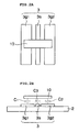
- Fig. 2A is a simplified illustration showing the relationship between the movable electrode 10 and the coplanar line 3 when viewed from the upper member 4.
- Fig. 2B is a simplified illustration showing the relationship between the movable electrode 10 and the coplanar line 3 when viewed from the side.
- the movable electrode 10 separated from and facing the signal line 3s and the ground lines 3g1 and 3g2 is arranged so as to cross the ground line 3g1, the signal line 3s, and the ground line 3g2.
- a protective insulating film 11 is arranged on the surface of the movable electrode 10.
- the insulating film 11 is made, for example, of a very thin insulating material such as silicon nitride (SiN) or other suitable material.
- the insulating film 11 has a thickness of, for example, approximately 0.1 ⁇ m.
- the upper member 4 has a recess 4a in a portion which faces the movable element 6, and fixed electrodes 12 (12a and 12b) which face the movable element 6 are provided on the internal surface of the recess 4a.
- Through holes 13a, 13b, and 13c are arranged in the surface of the upper member 4.
- the through holes 13a and 13b extend from the surface of the upper member 4 to the fixed electrodes 12a and 12b.
- the through hole 13c extends from the surface of the upper member 4 to the holder 8b.
- Electrode pads 14a, 14b, and 14c are arranged on the surface of the upper member 4 and are connected to the through holes 13a, 13b, and 13c, respectively.
- the movable element 6 is a high-resistivity semiconductor.
- the high-resistivity semiconductor functions as an insulator for the RF signal (for example, a signal of approximately 5 GHz or more) and functions as an electrode for a low-frequency signal (for example, a signal of approximately 100 kHz or less) and a DC signal.
- the high-resistivity semiconductor functioning as the movable element 6 has a resistance ranging from about 1,000 ⁇ cm to about 10,000 ⁇ cm, for example.
- the high-resistivity semiconductor has the following dielectric loss characteristics. As shown by the solid line B in Fig. 5, the higher the frequency, the larger the dielectric loss (tan ⁇ ) of an insulator made of glass or other suitable material. In contrast, as shown by the solid line A in Fig. 5, the higher the frequency, the smaller the dielectric loss of a high-resistivity semiconductor. In Fig. 5, the solid line A represents the dielectric loss of high-resistivity silicon having a resistance of approximately 2,000 ⁇ cm. Values in an area encircled by the solid line a are experimental values and the others are reference values. The values represented by the solid line B are reference values for Pyrex (registered trademark) glass.
- an RF signal of about 5 GHz or more flows in the coplanar line 3, and the dielectric loss characteristics with respect to the RF signal of the movable element 6 made of the high-resistivity semiconductor is equivalent to or superior to that of a movable element made of an insulator.
- the movable element 6 made of the high-resistivity semiconductor functions as the electrode for the DC signal (DC voltage).
- the movable element 6, functioning as the electrode, and the fixed electrodes 12a and 12b function as a movable element displacing unit for displacing the movable element 6.
- applying an external DC voltage for example, approximately 5 V
- the movable element 6 and the fixed electrodes 12 (12a and 12b) via the electrode pads 14a, 14b, and 14c and the through holes 13a, 13b, and 13c causes electrostatic attraction between the movable element 6 and the fixed electrodes 12.
- the movable element 6 is attracted towards the fixed electrodes 12 by this electrostatic attraction. Accordingly, the electrostatic attraction caused between the movable element 6 and the fixed electrodes 12 displaces the movable element 6.
- the RF-MEMS device 1 functions as a switching device for the coplanar line, as described below.
- the space between the movable electrode 10 and the coplanar line 3 is very small and the thickness of the space is substantially the same as the thickness of the insulating film 11 (for example, about 0.1 ⁇ m), thus increasing the capacitance between the movable electrode 10 and the coplanar line 3.
- Fig. 3A is an equivalent circuit diagram of the movable electrode 10 and the coplanar line 3 shown in Figs. 2A and 2B.
- C 1 represents the capacitance between the movable electrode 10 and the ground line 3g1
- C 2 represents the capacitance between the movable electrode 10 and the ground line 3g2
- C 3 represents the capacitance between the movable electrode 10 and the signal line 3s.
- L 1 and R 1 represent the inductance and resistance of the movable electrode 10 at the ground line 3g1 side, respectively.
- L 2 and R 2 represent the inductance and resistance of the movable electrode 10 at the ground line 3g2 side, respectively.
- the equivalent circuit shown in Fig. 3A can be represented as shown in Fig. 3B.
- the increase in the capacitance C between the movable electrode 10 and the coplanar line 3 due to the small space between the movable electrode 10 and the coplanar line 3 causes the series LC resonant frequency in the equivalent circuit shown in Fig. 3B to become close to the frequency of the RF signal flowing in the signal line 3s, thereby significantly reducing the impedance of the LC circuit when viewing the ground side from the signal line 3s side through the movable electrode 10.
- a state equivalent to a short circuit occurs when viewing the ground side from the signal line 3s side through the movable electrode 10. Accordingly, the signal conduction of the coplanar line 3 is switched off.
- the RF-MEMS device 1 can switch on or off the signal conduction of the coplanar line 3 by the displacement of the movable element 6 due to the electrostatic attraction.
- the movable element 6 is preferably made of the high-resistivity semiconductor.
- the movable element 6 itself can function as an electrode in the movable element displacing unit, as described above. With this function, there is no need to provide an electrode on the movable element 6 for the movable element displacing unit, thereby simplifying the structure and the manufacturing process of the RF-MEMS device 1. Consequently, the cost of the RF-MEMS device 1 can be reduced.
- the movable element 6 made of the high-resistivity semiconductor functions as an insulator for the RF signal, and the dielectric loss (tan ⁇ ) of the movable element 6 is substantially equal to or less than that of the insulator, thus reducing the propagation loss of the RF signal.
- the frequency of signals flowing in RF circuits has been higher.
- Increased dielectric loss of the movable element made of the insulator in the higher frequency range (refer to the solid line B in Fig. 5) disadvantageously increases the propagation loss of the signal by the movable element.
- the movable element 6 according to the first preferred embodiment is made of the high-resistivity semiconductor, the higher the frequency of the signal, the smaller the dielectric loss of the movable element 6 (refer to the solid line A in Fig. 5). Thus, the propagation loss of the signal by the movable element 6 is greatly reduced by increasing the frequency of the signal. Accordingly, the arrangement according to the first preferred embodiment will become very effective in the future.
- the resistance R in Fig. 3B increases by a contact resistance component added to the resistance R, thereby increasing the signal loss.
- the coplanar line 3 and the movable electrode 10 are coupled to each other with the capacitance therebetween. Thus, contact resistance does not occur between the coplanar line 3 and the movable electrode 10, thereby preventing and minimizing the signal loss.
- the RF-MEMS device 1 preferably has the same arrangement as in the first preferred embodiment with the exception that the movable element 6 is electrically floating. More specifically, the through hole 13c and the electrode pad 14c (see Figs. 1A and 1B) for allowing the movable element 6 to be conductively connected to the outside thereof are omitted in the second preferred embodiment. Accordingly, a much simpler structure can be achieved in the second preferred embodiment as compared to the structure according to the first preferred embodiment. Also, the manufacturing cost of the RF-MEMS device 1 can be reduced.
- the fixed electrodes 12 (12a and 12b) are arranged below the movable element 6. In other words, they are arranged on the substrate 2 to face part of the movable element 6.
- the upper member 4 (see Figs. 1B and 6) is omitted in the third preferred embodiment, unlike the first and second preferred embodiments in which the upper member 4 is provided in order to dispose the fixed electrodes 12 above the movable element 6.
- fixing units 16 (16a and 16b) fixed on the substrate 2 fix the movable element 6 by the beams 7 (7a and 7b) arranged between the movable element 6 and the fixing units 16.
- a DC voltage applied between the movable element 6 and the fixed electrodes 12 causes the movable element 6 to be attracted towards the substrate 2.
- a space is generated between the insulating film 11 on the movable electrode 10 and the coplanar line 3, as shown in Fig. 7.
- the upper member 4 is omitted, thus simplifying the structure and manufacturing process of the RF-MEMS device 1.
- the upper member 4 is omitted in the third preferred embodiment, even if the fixed electrodes 12 are arranged on the substrate 2 as in the third preferred embodiment, the upper member 4 may be arranged as in the first and second preferred embodiments for protecting the movable element 6.
- Fig. 8A is a schematic plan view showing the RF-MEMS device 1 according to the fourth preferred embodiment.
- Fig. 8B is a schematic sectional view showing the RF-MEMS device 1 taken along line A-A in Fig. 8A.
- the RF-MEMS device 1 according to each of the first, second, and third preferred embodiments functions as a so-called parallel switch
- the RF-MEMS device 1 according to the fourth preferred embodiment functions as a series switch.
- the signal line 3s of the coplanar line 3 has an intermediate gap 18, and the movable electrode 10 is arranged on the movable element 6 to face an area from one end of one divided line at one side of the intermediate gap 18 to one end of the other divided line at the other side of the intermediate gap 18, with the intermediate gap 18 therebetween.
- the movable electrode 10 does not face the ground line 3g1 and the ground line 3g2 of the coplanar line 3.
- the RF-MEMS device 1 preferably has the same arrangement as in the first, second, and third preferred embodiments with the exception of the arrangement of the signal line 3s of the coplanar line 3 and the movable electrode 10.
- the movable element 6 is connectable with an outside circuit via the through hole 13c and the electrode pad 14c as in the first preferred embodiment, the movable element 6 may be electrically floating, as in the second preferred embodiment.
- the fixed electrodes 12 are arranged on the upper member 4 in the fourth preferred embodiment, the fixed electrodes 12 may be arranged on the substrate 2, as in the third preferred embodiment.
- the movable electrode 10 connects the one end of each of the divided lines at both sides of the intermediate gap 18 and the signal conduction in the signal line 3s is thus switched on.
- the displacement of the movable element 6 by the movable element displacing unit causes the movable electrode 10 to be displaced away from the substrate 2, the space between the movable electrode 10 and the one end of each of the divided lines at both sides of the intermediate gap 18 becomes larger, thus reducing the capacitance between the movable electrode 10 and the one end of each of the divided lines at both sides of the intermediate gap 18. Accordingly, an open circuit occurs between the movable electrode 10 and the one end of each of the divided lines at both sides of the intermediate gap 18 and the signal conduction in the signal line 3s is thus switched off.
- the movable element 6 is also preferably made of a high-resistivity semiconductor, as in the first to third preferred embodiments, thus realizing advantages similar to those in the first to third preferred embodiments.
- the present invention is not limited to any of the first, second, third, and fourth preferred embodiments and various modifications may be applied thereto.
- the RF-MEMS device 1 is a switching device in the first to fourth preferred embodiments
- the RF-MEMS device 1 may be a variable capacitor having a similar structure.
- the movable element 6 must be significantly displaced so that the state between the movable electrode 10 and the coplanar line 3 can be switched between the RF short circuit and the open circuit.
- the variable capacitor however, the range of variation in the capacitance is generally not so large. Thus, it is unnecessary for the movable element 6 to be greatly displaced.
- the elastic modulus of the beams 7 and the like should preferably be set so that high-precision control for displacement of the movable element 6 can be realized.
- a coplanar line is preferably provided as an RF signal-conducting unit in the first to fourth preferred embodiments
- a microstrip line for example, may be provided as the RF signal-conducting unit.
- the movable element 6 may be composed of a high-resistivity semiconductor made, for example, of gallium arsenide (GaAs).
- GaAs gallium arsenide
- the insulating film 11 is arranged on the movable electrode 10 in the first to fourth preferred embodiments, the insulating film 11 may be arranged, for example, on a portion of the coplanar line 3 that faces at least the movable electrode 10 or may be arranged on a surface of the movable electrode 10 and a surface of the coplanar line 3, which face each other.
Landscapes
- Engineering & Computer Science (AREA)
- Power Engineering (AREA)
- Microelectronics & Electronic Packaging (AREA)
- Micromachines (AREA)
- Waveguide Switches, Polarizers, And Phase Shifters (AREA)
Claims (10)
- Dispositif MEMS à radiofréquence comprenant :un substrat (2) ;une unité conductrice de signal de radiofréquence (3) agencée sur le substrat, dans laquelle l'unité conductrice de signal de radiofréquence est une ligne coplanaire avec une ligne de signal (3s) et deux lignes de masse (3g1, 3g2), dans laquelle la ligne de signal est positionnée entre les lignes de masse mais n'est pas en contact avec elles ;un élément mobile (6) agencé au-dessus du substrat avec un espace entre eux et faisant face au moins à une partie de l'unité conductrice de signal de radiofréquence avec un espace entre eux ;une électrode mobile (10) agencée sur l'élément mobile et faisant face au moins à une partie de l'unité conductrice de signal de radiofréquence, où l'électrode mobile est agencée de manière à croiser les lignes de masse et la ligne de signal ;un élément supérieur (4) faisant face au moins à une partie d'une surface supérieure de l'élément mobile avec un espace entre eux ; etune électrode fixe (12) agencée sur l'élément supérieur de manière à faire face au moins à une partie de l'élément mobile ; dans lequell'élément mobile comprend un semi-conducteur à haute résistivité définissant un isolant pour un signal de radiofréquence et définissant une électrode pour un signal de basse fréquence et un signal de courant continu, l'électrode fixe et l'élément mobile sont agencés pour fonctionner ensemble et définir une unité de déplacement d'élément mobile pour déplacer l'élément mobile vers l'électrode fixe par attraction électrostatique provoquée par une tension de courant continue appliquée entre l'électrode fixe et l'élément mobile, l'unité de déplacement d'élément mobile déplace l'élément mobile vers ou à distance du substrat par l'attraction électrostatique, et le déplacement de l'élément mobile provoqué par l'unité de déplacement d'élément mobile change l'espace entre l'unité conductrice de signal de radiofréquence et l'électrode mobile de manière à varier la capacitance entre l'unité conductrice de signal de radiofréquence et l'électrode mobile.
- Dispositif MEMS à radiofréquence selon la revendication 1, comprenant en outre un film isolant protecteur (11) prévu sur au moins une d'une surface de l'unité conductrice de signal de radiofréquence (3) et d'une surface de l'électrode mobile (10), la surface de l'unité conductrice de signal de radiofréquence étant disposée opposée à ladite surface de l'électrode mobile.
- Dispositif MEMS à radiofréquence selon la revendication 1, dans lequel un signal de radiofréquence avec une fréquence d'au moins environ 5 GHz circule dans l'unité conductrice de signal de radiofréquence.
- Dispositif MEMS à radiofréquence selon la revendication 1, dans lequel le semi-conducteur à haute résistivité de l'élément mobile (6) présente une résistance allant d'environ 1 000 Ωcm à environ 10 000 Ωcm.
- Dispositif MEMS à radiofréquence selon la revendication 1, dans lequel le dispositif MEMS à radiofréquence est un condensateur variable défini par l'unité conductrice de signal de radiofréquence (3) et l'électrode mobile (10) et la capacitance du condensateur variable varie avec le déplacement de l'élément mobile (6).
- Dispositif MEMS à radiofréquence selon la revendication 1, dans lequel l'unité conductrice de signal de radiofréquence (3) est une ligne coplanaire, et dans lequel le dispositif MEMS à radiofréquence est un dispositif de commutation dans lequel une capacitance accrue entre la ligne coplanaire et l'électrode mobile (10) provoque un court-circuit de radiofréquence entre la ligne coplanaire et l'électrode mobile de manière à désactiver la conduction de la ligne coplanaire, et dans lequel une capacitance réduite entre la ligne coplanaire et l'électrode mobile provoque un circuit ouvert de radiofréquence entre la ligne coplanaire et l'électrode mobile de manière à activer la conduction de la ligne coplanaire.
- Dispositif MEMS à radiofréquence selon la revendication 1, dans lequel l'unité conductrice de signal de radiofréquence (3) comprend des lignes de signal divisées qui sont divisées par un espace intermédiaire prévue dans une zone qui fait face à l'électrode mobile (10), et une extrémité de chacune des lignes de signal divisées au niveau de chaque côté de l'espace intermédiaire fait face à l'électrode mobile avec un espace entre elles.
- Dispositif MEMS à radiofréquence selon la revendication 7, dans lequel le dispositif MEMS à radiofréquence est un dispositif de commutation dans lequel une capacitance accrue entre l'électrode mobile (10) et la première extrémité de chacune des lignes de signal divisées au niveau de chaque côté de l'espace intermédiaire provoque un court-circuit de radiofréquence entre l'électrode mobile et la première extrémité de chacune des lignes de signal divisées au niveau de chaque côté de l'espace intermédiaire de manière à activer la conduction de la première extrémité de chacune des lignes de signal divisées au niveau de chaque côté de l'espace intermédiaire par l'électrode mobile.
- Dispositif MEMS à radiofréquence selon la revendication 8, dans lequel une capacitance réduite entre l'électrode mobile (10) et la première extrémité de chacune des lignes de signal divisées au niveau de chaque côté de l'espace intermédiaire provoque un circuit ouvert entre l'électrode mobile et la première extrémité des lignes de signal au niveau de chaque côté de l'espace intermédiaire de manière à désactiver la conduction du signal dans les lignes de signal divisées.
- Dispositif MEMS à radiofréquence selon la revendication 1, dans lequel le dispositif MEMS à radiofréquence est un d'un dispositif de commutation et d'un condensateur variable.
Applications Claiming Priority (2)
| Application Number | Priority Date | Filing Date | Title |
|---|---|---|---|
| JP2002060765A JP3818176B2 (ja) | 2002-03-06 | 2002-03-06 | Rfmems素子 |
| JP2002060765 | 2002-03-06 |
Publications (3)
| Publication Number | Publication Date |
|---|---|
| EP1343189A2 EP1343189A2 (fr) | 2003-09-10 |
| EP1343189A3 EP1343189A3 (fr) | 2003-11-19 |
| EP1343189B1 true EP1343189B1 (fr) | 2006-06-07 |
Family
ID=27751143
Family Applications (1)
| Application Number | Title | Priority Date | Filing Date |
|---|---|---|---|
| EP03004086A Expired - Lifetime EP1343189B1 (fr) | 2002-03-06 | 2003-02-25 | Dispositif microélectroméchanique RF |
Country Status (4)
| Country | Link |
|---|---|
| US (1) | US6713695B2 (fr) |
| EP (1) | EP1343189B1 (fr) |
| JP (1) | JP3818176B2 (fr) |
| DE (1) | DE60305761T2 (fr) |
Families Citing this family (44)
| Publication number | Priority date | Publication date | Assignee | Title |
|---|---|---|---|---|
| JP3119255B2 (ja) * | 1998-12-22 | 2000-12-18 | 日本電気株式会社 | マイクロマシンスイッチおよびその製造方法 |
| US6919784B2 (en) | 2001-10-18 | 2005-07-19 | The Board Of Trustees Of The University Of Illinois | High cycle MEMS device |
| JP3709847B2 (ja) * | 2002-01-23 | 2005-10-26 | 株式会社村田製作所 | 静電型アクチュエータ |
| EP1343190A3 (fr) * | 2002-03-08 | 2005-04-20 | Murata Manufacturing Co., Ltd. | Elément à capacité variable |
| US6998946B2 (en) * | 2002-09-17 | 2006-02-14 | The Board Of Trustees Of The University Of Illinois | High cycle deflection beam MEMS devices |
| JP4066928B2 (ja) | 2002-12-12 | 2008-03-26 | 株式会社村田製作所 | Rfmemsスイッチ |
| DE10342938A1 (de) * | 2003-09-17 | 2005-04-21 | Bosch Gmbh Robert | Bauteil zu Impedanzänderung bei einem koplanaren Wellenleiter sowie Verfahren zu Herstellung eines Bauelements |
| KR100554468B1 (ko) * | 2003-12-26 | 2006-03-03 | 한국전자통신연구원 | 자기유지 중앙지지대를 갖는 미세 전자기계적 스위치 및그의 제조방법 |
| KR20050076149A (ko) * | 2004-01-19 | 2005-07-26 | 엘지전자 주식회사 | 압전 구동형 알에프 미세기전 시스템 스위치 및 그 제조방법 |
| US7352266B2 (en) * | 2004-02-20 | 2008-04-01 | Wireless Mems, Inc. | Head electrode region for a reliable metal-to-metal contact micro-relay MEMS switch |
| EP1729411A4 (fr) * | 2004-03-26 | 2009-07-15 | Mitsubishi Electric Corp | Circuit de phase, commutateur haute frequence et dispositif de phase |
| US7952534B2 (en) | 2004-03-31 | 2011-05-31 | Toto Ltd. | Microstrip antenna |
| US7652342B2 (en) * | 2004-06-18 | 2010-01-26 | Nantero, Inc. | Nanotube-based transfer devices and related circuits |
| US7499208B2 (en) * | 2004-08-27 | 2009-03-03 | Udc, Llc | Current mode display driver circuit realization feature |
| US7515147B2 (en) * | 2004-08-27 | 2009-04-07 | Idc, Llc | Staggered column drive circuit systems and methods |
| CN1295728C (zh) * | 2004-09-20 | 2007-01-17 | 东南大学 | 低阈值直交流可分的微电子机械开关及其制造方法 |
| CN1312718C (zh) * | 2004-09-21 | 2007-04-25 | 清华大学 | 一种多谐振点的微机械开关 |
| JP2006093463A (ja) | 2004-09-24 | 2006-04-06 | Toshiba Corp | 圧電mems素子及びチューナブルフィルタ |
| CN100403476C (zh) * | 2004-09-27 | 2008-07-16 | 东南大学 | 射频微电子机械单刀双掷膜开关及其制造方法 |
| KR100659298B1 (ko) | 2005-01-04 | 2006-12-20 | 삼성전자주식회사 | Mems 스위치 및 그 제조 방법 |
| JP4506529B2 (ja) | 2005-03-18 | 2010-07-21 | オムロン株式会社 | 静電マイクロスイッチおよびその製造方法、ならびに静電マイクロスイッチを備えた装置 |
| JP4707424B2 (ja) * | 2005-03-18 | 2011-06-22 | 株式会社東芝 | 可変容量素子および可変容量装置ならびに可変容量装置を用いた携帯電話 |
| KR100744543B1 (ko) * | 2005-12-08 | 2007-08-01 | 한국전자통신연구원 | 미세전자기계적 구조 스위치 및 그 제조방법 |
| KR20140079834A (ko) * | 2006-09-27 | 2014-06-27 | 가부시키가이샤 니콘 | 전자 소자, 가변 커패시터, 마이크로스위치, 마이크로스위치의 구동 방법, mems형 전자 소자, 마이크로 액추에이터 및 mems 광학 소자 |
| US7583169B1 (en) * | 2007-03-22 | 2009-09-01 | The United States Of America As Represented By The Administrator Of The National Aeronautics And Space Administration | MEMS switches having non-metallic crossbeams |
| JP4956312B2 (ja) * | 2007-07-20 | 2012-06-20 | 株式会社アドバンテスト | 遅延線 |
| JP4564549B2 (ja) * | 2008-05-01 | 2010-10-20 | 株式会社半導体理工学研究センター | Memsスイッチ |
| US20100001355A1 (en) * | 2008-07-07 | 2010-01-07 | Honeywell International Inc. | RF MEMS Switch |
| DK2230679T3 (da) | 2009-03-20 | 2012-07-30 | Delfmems | MEMS-struktur med en fleksibel membran og forbedrede elektriske påvirkningsmidler |
| CN102356440B (zh) | 2009-03-30 | 2013-12-25 | 株式会社村田制作所 | 可变电容模块及匹配电路模块 |
| KR20110062583A (ko) * | 2009-12-03 | 2011-06-10 | 주식회사 엠에스솔루션 | 고주파용 정전형 스위치 및 그 제조 방법 |
| JP5418316B2 (ja) | 2010-03-11 | 2014-02-19 | 富士通株式会社 | Memsデバイス |
| JP2011228355A (ja) * | 2010-04-15 | 2011-11-10 | Fujitsu Ltd | 可変容量素子および可変容量素子の製造方法 |
| CN102163516B (zh) * | 2011-01-10 | 2013-04-03 | 东南大学 | 一种无电荷注入效应高可靠性电容式射频微机电系统开关 |
| JP5542973B2 (ja) * | 2011-02-09 | 2014-07-09 | シャープ株式会社 | アクティブマトリクス基板、x線センサ装置、表示装置 |
| JP2013080790A (ja) * | 2011-10-03 | 2013-05-02 | Murata Mfg Co Ltd | 梁構造デバイス、および、その製造方法 |
| DE202012005934U1 (de) * | 2012-06-18 | 2012-07-10 | Rosenberger Hochfrequenztechnik Gmbh & Co. Kg | Schalter |
| US9520547B2 (en) | 2013-03-15 | 2016-12-13 | International Business Machines Corporation | Chip mode isolation and cross-talk reduction through buried metal layers and through-vias |
| US9219298B2 (en) | 2013-03-15 | 2015-12-22 | International Business Machines Corporation | Removal of spurious microwave modes via flip-chip crossover |
| US9954263B2 (en) | 2015-08-28 | 2018-04-24 | General Electric Company | Radio frequency micro-electromechanical systems having inverted microstrip transmission lines and method of making the same |
| US9570783B1 (en) * | 2015-08-28 | 2017-02-14 | General Electric Company | Radio frequency micro-electromechanical systems having inverted microstrip transmission lines and method of making the same |
| GB201815797D0 (en) * | 2018-09-27 | 2018-11-14 | Sofant Tech Ltd | Mems devices and circuits including same |
| US11962214B2 (en) * | 2019-05-28 | 2024-04-16 | B&R Industrial Automation GmbH | Transport device |
| US12283446B2 (en) | 2021-11-03 | 2025-04-22 | Samsung Electronics Co., Ltd. | Switch and electronic device including the same |
Citations (1)
| Publication number | Priority date | Publication date | Assignee | Title |
|---|---|---|---|---|
| US6143997A (en) * | 1999-06-04 | 2000-11-07 | The Board Of Trustees Of The University Of Illinois | Low actuation voltage microelectromechanical device and method of manufacture |
Family Cites Families (22)
| Publication number | Priority date | Publication date | Assignee | Title |
|---|---|---|---|---|
| JP3402642B2 (ja) * | 1993-01-26 | 2003-05-06 | 松下電工株式会社 | 静電駆動型リレー |
| US5479042A (en) * | 1993-02-01 | 1995-12-26 | Brooktree Corporation | Micromachined relay and method of forming the relay |
| US5619061A (en) * | 1993-07-27 | 1997-04-08 | Texas Instruments Incorporated | Micromechanical microwave switching |
| US5367585A (en) * | 1993-10-27 | 1994-11-22 | General Electric Company | Integrated microelectromechanical polymeric photonic switch |
| EP0892419B1 (fr) * | 1997-07-18 | 2005-11-16 | Northrop Grumman Corporation | Commutateur microélectromécanique |
| US5959338A (en) * | 1997-12-29 | 1999-09-28 | Honeywell Inc. | Micro electro-mechanical systems relay |
| JPH11274805A (ja) * | 1998-03-20 | 1999-10-08 | Ricoh Co Ltd | 高周波スイッチ並びに製造方法、及び集積化高周波スイッチアレイ |
| US6153839A (en) | 1998-10-22 | 2000-11-28 | Northeastern University | Micromechanical switching devices |
| JP3119255B2 (ja) | 1998-12-22 | 2000-12-18 | 日本電気株式会社 | マイクロマシンスイッチおよびその製造方法 |
| JP2000188049A (ja) | 1998-12-22 | 2000-07-04 | Nec Corp | マイクロマシンスイッチおよびその製造方法 |
| US6160230A (en) * | 1999-03-01 | 2000-12-12 | Raytheon Company | Method and apparatus for an improved single pole double throw micro-electrical mechanical switch |
| US6307452B1 (en) * | 1999-09-16 | 2001-10-23 | Motorola, Inc. | Folded spring based micro electromechanical (MEM) RF switch |
| CA2323189A1 (fr) | 1999-10-15 | 2001-04-15 | Cristian A. Bolle | Actionneur electrostatique a double mouvement pour micro-relais de systemes mecaniques microelectroniques |
| US6366186B1 (en) * | 2000-01-20 | 2002-04-02 | Jds Uniphase Inc. | Mems magnetically actuated switches and associated switching arrays |
| US6535091B2 (en) * | 2000-11-07 | 2003-03-18 | Sarnoff Corporation | Microelectronic mechanical systems (MEMS) switch and method of fabrication |
| US20020096421A1 (en) * | 2000-11-29 | 2002-07-25 | Cohn Michael B. | MEMS device with integral packaging |
| US20020124385A1 (en) | 2000-12-29 | 2002-09-12 | Asia Pacific Microsystem, Inc. | Micro-electro-mechanical high frequency switch and method for manufacturing the same |
| US6512300B2 (en) * | 2001-01-10 | 2003-01-28 | Raytheon Company | Water level interconnection |
| US6440767B1 (en) * | 2001-01-23 | 2002-08-27 | Hrl Laboratories, Llc | Monolithic single pole double throw RF MEMS switch |
| US6621387B1 (en) * | 2001-02-23 | 2003-09-16 | Analatom Incorporated | Micro-electro-mechanical systems switch |
| US6472962B1 (en) * | 2001-05-17 | 2002-10-29 | Institute Of Microelectronics | Inductor-capacitor resonant RF switch |
| US6426687B1 (en) * | 2001-05-22 | 2002-07-30 | The Aerospace Corporation | RF MEMS switch |
-
2002
- 2002-03-06 JP JP2002060765A patent/JP3818176B2/ja not_active Expired - Lifetime
-
2003
- 2003-02-24 US US10/372,697 patent/US6713695B2/en not_active Expired - Lifetime
- 2003-02-25 DE DE60305761T patent/DE60305761T2/de not_active Expired - Lifetime
- 2003-02-25 EP EP03004086A patent/EP1343189B1/fr not_active Expired - Lifetime
Patent Citations (1)
| Publication number | Priority date | Publication date | Assignee | Title |
|---|---|---|---|---|
| US6143997A (en) * | 1999-06-04 | 2000-11-07 | The Board Of Trustees Of The University Of Illinois | Low actuation voltage microelectromechanical device and method of manufacture |
Also Published As
| Publication number | Publication date |
|---|---|
| DE60305761D1 (de) | 2006-07-20 |
| DE60305761T2 (de) | 2006-10-19 |
| JP3818176B2 (ja) | 2006-09-06 |
| US20030169146A1 (en) | 2003-09-11 |
| EP1343189A3 (fr) | 2003-11-19 |
| US6713695B2 (en) | 2004-03-30 |
| EP1343189A2 (fr) | 2003-09-10 |
| JP2003258502A (ja) | 2003-09-12 |
Similar Documents
| Publication | Publication Date | Title |
|---|---|---|
| EP1343189B1 (fr) | Dispositif microélectroméchanique RF | |
| US7126447B2 (en) | RF-mems switch | |
| US7027284B2 (en) | Variable capacitance element | |
| JP3890952B2 (ja) | 容量可変型キャパシタ装置 | |
| US6153839A (en) | Micromechanical switching devices | |
| JP4262199B2 (ja) | 微小電気機械スイッチ | |
| EP1560787B1 (fr) | Dispositif a mems equipe d'un actionneur piezo-electrique en couche mince | |
| US7545081B2 (en) | Piezoelectric RF MEMS device and method of fabricating the same | |
| US20070278075A1 (en) | Capacitance Type Mems Device, Manufacturing Method Thereof, And High Frequency Device | |
| KR100492004B1 (ko) | 미세전자기계적 시스템 기술을 이용한 고주파 소자 | |
| KR20010030305A (ko) | 접이식 스프링을 구비한 초소형 전기 기계 고주파 스위치및 그 제조 방법 | |
| EP2144265A1 (fr) | Commutateur MEMS RF | |
| US7554421B2 (en) | Micro-electromechanical system (MEMS) trampoline switch/varactor | |
| KR20050076149A (ko) | 압전 구동형 알에프 미세기전 시스템 스위치 및 그 제조방법 | |
| EP1642311A2 (fr) | Dispositif microelectromecanique, module et leur procede de fabrication | |
| JP3137112B2 (ja) | マイクロマシンスイッチおよびその製造方法 | |
| WO2003015128A2 (fr) | Commutateur electromecanique et procede de fabrication correspondant | |
| US20060091983A1 (en) | Electrostatic microswitch for low-voltage-actuation component | |
| KR100378356B1 (ko) | Rf 차단 레지스터를 이용한 mems 스위치 | |
| US6624367B1 (en) | Micromachine switch | |
| KR100493532B1 (ko) | 정전식 양방향 미세기전 액추에이터 | |
| KR20020074331A (ko) | Rf 차단 레지스터를 이용한 mems 스위치 | |
| JP5130291B2 (ja) | 電気機械素子およびそれを用いた電気機器 | |
| KR100357164B1 (ko) | 마이크로 가변 커패시터 |
Legal Events
| Date | Code | Title | Description |
|---|---|---|---|
| PUAI | Public reference made under article 153(3) epc to a published international application that has entered the european phase |
Free format text: ORIGINAL CODE: 0009012 |
|
| 17P | Request for examination filed |
Effective date: 20030225 |
|
| AK | Designated contracting states |
Kind code of ref document: A2 Designated state(s): AT BE BG CH CY CZ DE DK EE ES FI FR GB GR HU IE IT LI LU MC NL PT SE SI SK TR |
|
| AX | Request for extension of the european patent |
Extension state: AL LT LV MK RO |
|
| PUAL | Search report despatched |
Free format text: ORIGINAL CODE: 0009013 |
|
| AK | Designated contracting states |
Kind code of ref document: A3 Designated state(s): AT BE BG CH CY CZ DE DK EE ES FI FR GB GR HU IE IT LI LU MC NL PT SE SI SK TR |
|
| AX | Request for extension of the european patent |
Extension state: AL LT LV MK RO |
|
| 17Q | First examination report despatched |
Effective date: 20040406 |
|
| AKX | Designation fees paid |
Designated state(s): DE FR GB |
|
| GRAP | Despatch of communication of intention to grant a patent |
Free format text: ORIGINAL CODE: EPIDOSNIGR1 |
|
| GRAS | Grant fee paid |
Free format text: ORIGINAL CODE: EPIDOSNIGR3 |
|
| GRAA | (expected) grant |
Free format text: ORIGINAL CODE: 0009210 |
|
| AK | Designated contracting states |
Kind code of ref document: B1 Designated state(s): DE FR GB |
|
| REG | Reference to a national code |
Ref country code: GB Ref legal event code: FG4D |
|
| REF | Corresponds to: |
Ref document number: 60305761 Country of ref document: DE Date of ref document: 20060720 Kind code of ref document: P |
|
| ET | Fr: translation filed | ||
| PLBE | No opposition filed within time limit |
Free format text: ORIGINAL CODE: 0009261 |
|
| STAA | Information on the status of an ep patent application or granted ep patent |
Free format text: STATUS: NO OPPOSITION FILED WITHIN TIME LIMIT |
|
| 26N | No opposition filed |
Effective date: 20070308 |
|
| REG | Reference to a national code |
Ref country code: FR Ref legal event code: PLFP Year of fee payment: 14 |
|
| REG | Reference to a national code |
Ref country code: FR Ref legal event code: PLFP Year of fee payment: 15 |
|
| REG | Reference to a national code |
Ref country code: FR Ref legal event code: PLFP Year of fee payment: 16 |
|
| PGFP | Annual fee paid to national office [announced via postgrant information from national office to epo] |
Ref country code: GB Payment date: 20220223 Year of fee payment: 20 Ref country code: DE Payment date: 20220217 Year of fee payment: 20 |
|
| PGFP | Annual fee paid to national office [announced via postgrant information from national office to epo] |
Ref country code: FR Payment date: 20220216 Year of fee payment: 20 |
|
| REG | Reference to a national code |
Ref country code: DE Ref legal event code: R071 Ref document number: 60305761 Country of ref document: DE |
|
| REG | Reference to a national code |
Ref country code: GB Ref legal event code: PE20 Expiry date: 20230224 |
|
| PG25 | Lapsed in a contracting state [announced via postgrant information from national office to epo] |
Ref country code: GB Free format text: LAPSE BECAUSE OF EXPIRATION OF PROTECTION Effective date: 20230224 |