EP2144360B1 - Procédé de fonctionnement d'un convertisseur de courant et dispositif correspondant - Google Patents
Procédé de fonctionnement d'un convertisseur de courant et dispositif correspondant Download PDFInfo
- Publication number
- EP2144360B1 EP2144360B1 EP08012314.4A EP08012314A EP2144360B1 EP 2144360 B1 EP2144360 B1 EP 2144360B1 EP 08012314 A EP08012314 A EP 08012314A EP 2144360 B1 EP2144360 B1 EP 2144360B1
- Authority
- EP
- European Patent Office
- Prior art keywords
- semiconductor switches
- lower semiconductor
- converter
- network
- power supply
- Prior art date
- Legal status (The legal status is an assumption and is not a legal conclusion. Google has not performed a legal analysis and makes no representation as to the accuracy of the status listed.)
- Not-in-force
Links
- 238000000034 method Methods 0.000 title claims description 35
- 239000004065 semiconductor Substances 0.000 claims description 153
- 238000005259 measurement Methods 0.000 claims description 40
- 230000000694 effects Effects 0.000 claims description 17
- 238000012360 testing method Methods 0.000 claims description 17
- 230000003213 activating effect Effects 0.000 claims description 14
- 238000004590 computer program Methods 0.000 claims description 10
- 238000012937 correction Methods 0.000 claims description 10
- 238000012545 processing Methods 0.000 claims description 4
- 230000004913 activation Effects 0.000 description 26
- 239000004020 conductor Substances 0.000 description 8
- 230000008901 benefit Effects 0.000 description 5
- 238000010586 diagram Methods 0.000 description 5
- 230000009467 reduction Effects 0.000 description 5
- 230000008859 change Effects 0.000 description 4
- 230000006870 function Effects 0.000 description 4
- 238000013459 approach Methods 0.000 description 3
- 230000007423 decrease Effects 0.000 description 3
- 230000001419 dependent effect Effects 0.000 description 3
- 238000011156 evaluation Methods 0.000 description 3
- 230000008569 process Effects 0.000 description 3
- 230000007704 transition Effects 0.000 description 3
- 239000003990 capacitor Substances 0.000 description 2
- 238000001514 detection method Methods 0.000 description 2
- 230000005284 excitation Effects 0.000 description 2
- 238000004519 manufacturing process Methods 0.000 description 2
- 238000012821 model calculation Methods 0.000 description 2
- 230000004048 modification Effects 0.000 description 2
- 238000012986 modification Methods 0.000 description 2
- 230000001172 regenerating effect Effects 0.000 description 2
- 230000002441 reversible effect Effects 0.000 description 2
- 230000009466 transformation Effects 0.000 description 2
- 238000012935 Averaging Methods 0.000 description 1
- 230000009471 action Effects 0.000 description 1
- 230000003139 buffering effect Effects 0.000 description 1
- 238000004364 calculation method Methods 0.000 description 1
- 239000003795 chemical substances by application Substances 0.000 description 1
- 238000011161 development Methods 0.000 description 1
- 230000018109 developmental process Effects 0.000 description 1
- 230000004069 differentiation Effects 0.000 description 1
- 230000007613 environmental effect Effects 0.000 description 1
- ZINJLDJMHCUBIP-UHFFFAOYSA-N ethametsulfuron-methyl Chemical compound CCOC1=NC(NC)=NC(NC(=O)NS(=O)(=O)C=2C(=CC=CC=2)C(=O)OC)=N1 ZINJLDJMHCUBIP-UHFFFAOYSA-N 0.000 description 1
- 230000002349 favourable effect Effects 0.000 description 1
- 238000010304 firing Methods 0.000 description 1
- 238000009499 grossing Methods 0.000 description 1
- 230000007935 neutral effect Effects 0.000 description 1
- 230000003071 parasitic effect Effects 0.000 description 1
- 230000008929 regeneration Effects 0.000 description 1
- 238000011069 regeneration method Methods 0.000 description 1
- 230000035945 sensitivity Effects 0.000 description 1
- 230000001360 synchronised effect Effects 0.000 description 1
- 230000002123 temporal effect Effects 0.000 description 1
- 230000001960 triggered effect Effects 0.000 description 1
Images



Classifications
-
- H—ELECTRICITY
- H02—GENERATION; CONVERSION OR DISTRIBUTION OF ELECTRIC POWER
- H02M—APPARATUS FOR CONVERSION BETWEEN AC AND AC, BETWEEN AC AND DC, OR BETWEEN DC AND DC, AND FOR USE WITH MAINS OR SIMILAR POWER SUPPLY SYSTEMS; CONVERSION OF DC OR AC INPUT POWER INTO SURGE OUTPUT POWER; CONTROL OR REGULATION THEREOF
- H02M7/00—Conversion of AC power input into DC power output; Conversion of DC power input into AC power output
- H02M7/02—Conversion of AC power input into DC power output without possibility of reversal
- H02M7/04—Conversion of AC power input into DC power output without possibility of reversal by static converters
- H02M7/12—Conversion of AC power input into DC power output without possibility of reversal by static converters using discharge tubes with control electrode or semiconductor devices with control electrode
- H02M7/21—Conversion of AC power input into DC power output without possibility of reversal by static converters using discharge tubes with control electrode or semiconductor devices with control electrode using devices of a triode or transistor type requiring continuous application of a control signal
- H02M7/217—Conversion of AC power input into DC power output without possibility of reversal by static converters using discharge tubes with control electrode or semiconductor devices with control electrode using devices of a triode or transistor type requiring continuous application of a control signal using semiconductor devices only
- H02M7/219—Conversion of AC power input into DC power output without possibility of reversal by static converters using discharge tubes with control electrode or semiconductor devices with control electrode using devices of a triode or transistor type requiring continuous application of a control signal using semiconductor devices only in a bridge configuration
Definitions
- the present invention relates to a method for operating a fundamental frequency clocked, network-side converter with a bridge circuit equipped with controllable semiconductor switches and an apparatus provided for carrying out the method, ie a converter device with such a converter and such a bridge circuit.
- the power converter has two self-commutated six-pulse bridge circuits (one network-side and one machine-side) as well as a DC voltage intermediate circuit.
- the line-side voltage is usually determined, with voltage sensors being used.
- the presented method now shows that it is possible to dispense with the conventional measurement of the phase voltages on the network and thus the voltage sensors for the synchronization of the network-side six-pulse bridge circuits with the network.
- a current flow is determined in the individual network phases, while the power semiconductors of the six-pulse bridge circuits are in a usual freewheeling state for self-commutated inverters (space vector zero) of a pulse width modulated control.
- a converter device or a converter circuit comprises at least one mains connection and strands acting as a current connection, when connecting to a three-phase network three strings, then the actual converter with the bridge circuit implementing the current direction functionality and at the output of the converter a DC link Output of the power converter form a first DC link contact and a second output of the power converter form a second DC link contact.
- an intermediate circuit voltage is present between these two DC link contacts, which results as DC voltage due to the current direction.
- a DC link capacitance is usually arranged between the DC link contacts.
- the power converter operates approximately as a so-called B6 diode bridge, since only the diodes included by the power converter carry the current and each antiparallel arranged as a semiconductor switch transistors are de-energized. Conversely, with power flow from the intermediate circuit in the network, the diodes in the reverse direction and the current is enabled by appropriate activation of individual transistors at any time exactly one path into the network.
- a preferred circuit for the converter forming the bridge circuit is a so-called IGBT B6 bridge (Insulated Gate Bipolar Transistor), which includes a passive parallel diode bridge, a purely passive operation in a power direction, ie, for. B.
- Switching edges for driving the transistors which are generally referred to below as semiconductor switches, are in fundamental frequency operation at so-called natural ignition times, ie intersections the mains voltages that are supplied to the circuit or the device via the individual current paths, in a three-phase network, ie the individual, hereinafter referred to as R, S, T lines of the three-phase network with the above supplied mains voltages U R , U S and U T.
- the fundamental-frequency clocked operation of power converters is characterized by a number of advantages that make the application useful. Since no high-frequency clocking of denoted as current valves semiconductor switch, resulting, for example, low switching losses and further the possibility of using simple and inexpensive commutation and line filters and finally a small excitation of system vibrations, the z. B. can lead to high engine bearing currents. Finally, the operation of such converters is generally robust to mains disturbances, network imbalances and the like.
- the switching edges of the semiconductor switches in fundamental frequency operation are at the natural ignition times defined by the intersections of the mains voltages.
- the knowledge of the network phase position is required.
- For this comparatively expensive measuring methods have hitherto been proposed according to the prior art, for. B. an evaluation of a conductor-to-conductor voltage in the converter or a detection of the time of a sign change of these voltages by means of a comparator circuit.
- the measuring devices required for such measurements are neither for the actual inverter function nor for the protection of the inverter required and could be omitted insofar as it was possible to implement another solution for determining the network phase position.
- the upper semiconductor switches in a three-phase network three upper semiconductor switches, are connected to a first DC link contact and the lower semiconductor switches, in a three-phase network corresponding to three lower semiconductor switches are connected to a second DC link contact, wherein the first and second DC link contact in the operation of the power converter on a first or lie second DC link potential.
- the simultaneous activity of at least two upper or lower Semiconductor switch results during a not necessarily uninterrupted period of predetermined or predeterminable duration before and / or after such times that correspond to the resulting due to a network angle natural ignition timing of the semiconductor switches in fundamental frequency operation.
- the simultaneous activation of at least two semiconductor switches means that at least one further semiconductor switch is activated in addition to the semiconductor switch which is normally active due to the fundamental frequency clocking.
- the advantage of the invention is that the simultaneous activation of two upper or lower semiconductor switches of the bridge circuit and, in conjunction with the anti-parallel diodes, electrically results in a mesh and thus a closed circuit. With respect to this circuit, measurements, in particular current measurements, can be carried out, the result of which can be used to track the network angle.
- Advantageous embodiments of the invention are the subject of the dependent claims.
- the relationships used here indicate the further development of the subject matter of the independent claim (s) by the features of the respective subclaim; they should not be construed as a waiver of obtaining independent, objective protection for the feature combinations of the dependent claims.
- the simultaneously activated upper or lower semiconductor switches are those semiconductor switches between which a switching occurs in fundamental frequency operation, it is advantageous that in the region of a sector boundary for switching in fundamental frequency operation that conductor-conductor voltage is small, switched between their phases shall be; in a three-phase network, the voltage of the respective third phase is then in the range of its maximum and changes only relatively slowly. For the determination of the phase position, that is to say for tracking the estimated network angle, it is therefore approximately sufficient to consider the mesh short-circuited by the simultaneous activation of the upper or lower semiconductor switches.
- each string to a center tap between each of an upper and a lower semiconductor switch.
- the tracking of the estimated network angle takes place with respect to a total voltage in the strings connected via the simultaneously activated semiconductor switches.
- the respectively simultaneously controlled semiconductor switch so that each connected strands are combined into a mesh and this results in the total voltage, the sum of a conductor-to-conductor voltage between the two meshed strands plus the voltage drop along the respective strand, so z.
- the voltage across the commutation reactor included in the string decreases. If saturation effects, e.g. B.
- a peak value of the chained network voltages based on a middle between the first and second DC link contact voltage applied DC link voltage is approximately known. from that An estimate of the terminal voltage at the time of the measurements to be taken can be obtained using the current grid frequency estimate. This can be used to determine a deviation from the voltage estimation value, which can be positive or negative and is a measure of whether the switch-on process was too early or too late compared to the actual sector boundary, ie in comparison to the real network angle. Accordingly, this deviation may be used as input to a phase locked loop (PLL) to increase or decrease the estimate of the line frequency.
- PLL phase locked loop
- the tracking of the estimated network angle can thus take place either linearly with a correction value formed on the basis of the total voltage or in discrete steps on the basis of a sign of the total voltage or of a correction value formed therefrom.
- the task outlined above is achieved analogously with a power converter device according to claim 6.
- the simultaneous activation of two upper or lower semiconductor switches is thereby triggered during a predetermined or predetermined, not necessarily uninterruptible period of time before and / or due to a network angle resulting natural ignition timing of the semiconductor switch in fundamental frequency operation.
- the advantage of such an embodiment of the converter device corresponds analogously to the advantages described above for the method according to the invention. In that regard, reference is made to the explanations already given above.
- the power converter is connected to mains side strands and indeed each strand to a center tap between a respective upper and a lower semiconductor switch
- the tracking of the estimated network angle with respect to a total voltage in the connected via the simultaneously activated semiconductor switch strands form a mesh and thus a closed circuit in which the measurements for tracking the estimated network angle are performed.
- a selectable plurality of patterns for the simultaneous activation of two upper or lower semiconductor switches is deposited. This can be used for the simultaneous activation of two lower and upper semiconductor switch different waveforms in which each pattern z. B. causes favorable effects for individual operating and environmental situations.
- the method outlined above and explained in more detail below is preferably implemented in software and / or firmware (microcode according to VHDL or the like in FPGA, ASIC or the like), so that the invention also provides a computer program with computer-executable program code instructions or Concerns microcode instructions.
- the invention then also relates to a storage medium having a computer program executable such computer program and a power converter device on which such a computer program is loaded.
- the invention thus also relates to a converter device with a processing unit in the manner of a processor or the like as a means for simultaneous Activation of two upper or lower semiconductor circuit and as a means for performing two measurements during the simultaneous activity of two upper or lower semiconductor switches and as a means for deriving a tracking of an estimated network angle for clocking the semiconductor switches based on the measurements, wherein on the processing unit a computer program as outlined above loaded and / or wherein the processing unit is intended and provided for the execution of such a computer program.
- FIG. 1 shows schematically simplified the connection and the structure of a power converter 10 to a three-phase network 12, wherein the power converter 10 equipped with controllable semiconductor switches T1, T2, T3, T4, T5, T6 and anti-parallel diodes D1, D2, D3, D4, D5, D6 Bridge circuit, in particular in an embodiment as an IGBT B6 bridge comprises.
- the converter 10 is followed by an intermediate circuit 14 at its output, which comprises a DC link capacitance 16, over which an intermediate circuit voltage u DC drops during operation.
- the DC link capacitance 16 is also referred to as C DC according to common circuit element designations.
- a number of upper semiconductor switches T1-T3, in the illustrated case exactly three upper semiconductor switches T1-T3, with a in operation of the power converter 10 on a first DC link potential lying first DC link contact 18 is connected.
- a number of lower semiconductor switches T4-T6, in the illustrated case exactly three lower semiconductor switches T4-T6, are connected to a second intermediate circuit contact 20 which is at a second intermediate circuit potential during operation of the power converter 10.
- Between the first and the second DC link contact 18, 20 of the DC link capacitor 16 is connected and the potential difference between the voltage applied to these contacts 18, 20 potentials corresponds to the intermediate circuit voltage u DC .
- the input side of the power converter 10 is connected to the network 12, via network-side strands 22, 24, 26 in such a way that each strand 22-26 is connected to a center tap between a respective upper and a lower semiconductor switch T1-T6.
- Each strand comprises a commutating 22-26 C L and in each strand 22-26 flows through the certain line voltages u R, u S, u T current i R, i S, i T.
- For the feeding network 12 is shown for each phase R, S, T each have a network inductance L network .
- Switching edges for driving the semiconductor switches T1-T6 are for fundamental frequency operation at so-called natural ignition times, namely the intersections of the sinusoidal mains voltages u R , u S , u T or the zero crossings of the phase-to-phase voltages u RS , u ST and u TR ,
- FIG. 2 is schematically simplified to explain a control logic of the semiconductor switches T1-T6 in fundamental frequency operation, a network period of 0 ° -360 ° shown, the illustration on the left side of FIG. 2 hereinafter referred to as a sector diagram and in which sector boundaries (at 0 °, 60 °, 120 °, 180 °, 240 °, 300 °) in each case a switching (commutation) takes place between two semiconductor switches T1-T6, at the sector boundary at 0 ° eg between the semiconductor switches designated T5 and T6.
- the power converter 10 works approximately like a B6 diode bridge, since the diodes D1-D6 carry the current and the respective antiparallel arranged semiconductor switches T1-T6 are de-energized.
- the diodes D1-D6 are in the reverse direction and the current is exactly at any time a path through each active semiconductor switches T1-T6 in the network 12 allows.
- This sketched operating mode (power flow into or out of the intermediate circuit 14) is characterized by a number of advantages which make the use of such a power converter 10 sensible. Since no high-frequency clocking of the acting as a flow control valve semiconductor switches T1-T6, z. B. lower switching losses, simple and inexpensive commutation L C and line filters and lower excitation of system vibrations, the z. B. can lead to high engine bearing currents and finally a robust operation in power disturbances, Netzunsymmetrien and the like. Due to the properties mentioned, such fundamental frequency clocked power converters 10 are particularly suitable for applications where cost-effective solutions are sought and high cost pressure prevails. Therefore, there is a particular need for cost reduction measures. Effective are corresponding changes to the structure or circuit, as they are effective in production for each single device and thus allow in total large savings.
- FIG. 2 shows, for the correct control of the semiconductor switches T1-T6, the knowledge of the phase position of the network 12 (network phase position) is required. While the network phase position can be determined by measurement on the basis of additional measuring devices, according to the invention a method for determining the network phase position and a device operating according to the method are proposed which, in addition to measuring devices which are already essential for the actual converter function or the converter protection, none further, provided exclusively for the determination of the phase position measuring devices.
- the determination of the network phase position in operation has hitherto been based on a direct measurement of the mains voltage, eg by measuring at least two phase-to-phase voltages at the converter terminals, and thus requires an A / D converter, a ⁇ converter or the like, or by detecting a sign change of the phase-to-phase voltages by means of a special comparator circuit or by measuring at least two phase-to-phase voltages on the network side of the commutation reactor In turn, for example, requires a separate measurement module with A / D converter at the grid connection point.
- the current network angle can be calculated directly by suitable transformation.
- This instantaneous value can be supplied as the input value of a PLL operating with an estimate for the network angle in order to track the network frequency or a PLL estimated value of the network angle.
- the network angle is known at exactly the time of a zero crossing. Between the times of the voltage zero crossings, the network angle can be easily interpolated.
- the interpolation value is used as the input value of a network PLL (sa 2005E18911 DE ) to obtain a filtered continuous estimate of the line frequency.
- FIG. 3 shows a schematically simplified block diagram of a configured according to the invention converter device for a model-based determination of the network phase angle. This shows, compare also FIG. 1 , the network 12, the commutation inductors L C , the power converter 10 and the intermediate circuit 14 with the intermediate circuit capacity 16, and arranged between the network 12 and intermediate circuit 14 power converter 10th
- activating agent means 30 for distinguishing means for activating the semiconductor switches T1-T6 corresponding to the fundamental frequency operation, ie to the natural ignition timing, and on the other hand for simultaneous activation of two upper or lower semiconductor switches T1-T3; T5-T6 of the power converter 10 is provided.
- the activation of the semiconductor switches T1-T3; T5-T6 takes place by activation signals 32.
- the simultaneous activation takes place during a predetermined or predefinable period of time before and / or after natural ignition times of the semiconductor switches T1-T6 resulting from a network angle in fundamental frequency operation.
- the measuring means 34 or the measuring means 34 take over the measurement of the phase currents i R , i S , i T and on this basis a model-based evaluation of changes in the measured currents at the time of suitable switching signals.
- the one or more measuring means 34 provides as an output an estimation error 36 which is fed to a frequency estimator (model) 38 as means for deriving a tracking of an estimated network angle 40.
- the tracking takes place on the basis of the measurements effected by the measuring device or means 34 and the thus corrected, possibly corrected, estimated network angle 40 is used to clock the semiconductor switches T1-T6 and for this purpose the activating means 30 and there an adjustment means 42 for Tracking a previously estimated network angle used to drive the semiconductor switches T1-T6.
- the estimation error 36 thus serves as an input to the model acting frequency estimator 38 (preferably implemented as a PLL) and an output generated by the frequency estimator 38 is used as the estimated network angle 40 for tracking line frequency and phase angle (line phasing).
- Measuring means 34, model 38 and activating means 30 are preferably implemented in software and / or firmware. Accordingly, a processor, ASIC, FPGA or the like (not shown separately) which execute such a software or firmware also come into consideration as measuring means 34, model 38 and activating means 30.
- the method is initially described using the example of the commutation process at the transition from the activation of the first designated as T1 semiconductor switch for activating the designated as T2 semiconductor switch (T1 ⁇ T2, corresponding to the sector boundary at 60 ° in FIG. 2 ) in the upper bridge branch.
- the semiconductor switch T6 in the lower branch remains permanent in this period switched on.
- the "normal" drive signals 32 ( FIG. 3 ) according to the fundamental frequency clocking are in FIG. 4 shown, wherein over the time t, the drive signals 32 are shown for driving two semiconductor switches, in an upper illustration for a semiconductor switch to be turned on and in a lower illustration for a semiconductor switch to be switched off. Switching takes place at the sector boundary 44 illustrated by a vertical line.
- FIG. 4 shows the situation that eg at a network angle of 60 °, ie at the transition from sector I to sector II (cf. FIG. 2 ), the semiconductor switches called T1 and T2 are turned off and on at the same time.
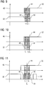
- FIG. 5 shows FIG. 5 a snapshot when driving two semiconductor switches T1-T6 according to the approach of the invention.
- Two switched according to the natural firing times and turned OFF semiconductor switches T1-T6 are the same at least for a short period of time active, and although in the illustrated case from that for a time t 0 adopted sector boundary 44.
- an overlap or overlap phase designated be simultaneous activity carried out two measurements whose result for tracking the estimated network angle 40 (FIG. FIG. 3 ) is used to clock the semiconductor switches T1-T6.
- a first measurement 48 represented by a hatched area takes place at a time t 1 during the overlap, and a second measurement 50 takes place at a time t 2 during the overlap.
- Equation 1 The voltage drops at the semiconductor switches T1-T6 and other parasitic effects were approximately neglected in Equation 1, as were the voltage drops at the network inductance L network (cf. FIG. 1 ).
- the network inductance can be added to the commutation inductance L C. Saturation effects of the commutation reactor as a function of the current may need to be considered.
- This deviation can be positive or negative and is a measure of whether the turn-on operation of the transistor T2 was too early or too late compared to the actual sector limit (or compared to the actual network angle). Accordingly, this signal can be used as input to a PLL to increase or decrease the estimate of the line frequency.
- the conductor-to-conductor voltage is small, between which phases should be switched.
- the voltage of the respective third phases is then in the range of their maximum and changes only relatively slowly.
- the voltage u T acts on the current path of the turned-on lower semiconductor switch, here the transistor T6, and the DC link capacitor 16 approximately symmetrically to the phases R and S. Therefore, for the determination of the phase position is approximately the sole consideration of the shorted mesh 52nd sufficient over u RS (Equation 1).
- y RS as an error measure for the network synchronization
- u RS, setpoint ( t 12 ) 0 or u R
- setpoint u S
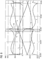
- FIG. 8 shows by way of example the case of a too early commutation from a first upper semiconductor switch to a second upper semiconductor switch, here from the transistor T1 to the transistor T2, as would occur for a too high estimated network frequency. Shown are the current and voltage curves on the example of a - based on the marked sector boundary 44 - too early switching with an overlap of the turn-on in the hatched area.
- the effective network voltage u RS at the two measurement times is no longer the same amount and leads to different current changes of i R and i S. It results a y RS ⁇ 0 as a characteristic of an over-estimated network frequency in a transistor of the upper half of the bridge.
- the error voltages y are determined at every sector change and thus six times per network period. To achieve a stable and robust estimation of line frequency and angle using a PLL, the error values can still be filtered. It may also make sense to set a tolerance band of permissible error values in order to compensate for model inaccuracies. In a preferred embodiment, only the sign information of the error voltage signum ( y ) can also be used as the input value of a discrete frequency estimator 38 (FIG. FIG. 3 ) serve. The frequency estimate in frequency estimator 38 would accordingly be incremented or decremented and used for switching at the next sector boundary.
- the normal control of the semiconductor switches T1-T6 for the fundamental frequency clocking ( FIG. 2 ) is extended so that at times two switches of a half bridge, so two upper or lower semiconductor switches T1-T3; T5-T6, activated at the same time, ie closed.
- current changes in the affected network phases are measured, eg by at least two consecutive current measurements.
- a measure is calculated which indicates a quality criterion for the desired position of the switching action with respect to the actual actual network phase angle.
- the quality measure serves as an input or correction value for a network frequency / network angle frequency estimator 38 (preferably a PLL).
- the network angle 40 calculated by the frequency estimator 38 is used for the generation of the activation signals 32 and for the generation of the said supplementary signals (simultaneous closing of several switches of a half-bridge). Due to the closed control loop for the model-based tracking of the network angle 40 can be dispensed with measuring sockets (A / D converter, comparators, etc) for the direct determination of the mains voltage or the sign change of the mains voltages.
- the quality value may be used quantitatively to correct the frequency estimate 40 in a frequency estimator 38.
- the current changes must be measurable in at least two phases (measuring device only required in two phases).
- an error value can be calculated to evaluate the actual network angle location and used to increase model accuracy (eg, by averaging the quality value from the first mesh equation).
- the method described so far regards the tracking of the estimated network angle during operation, that is to say, with already running clocking of the semiconductor switches. What is not described here is how a first synchronization occurs, that is, how the network angle and frequency can be accurately determined prior to enabling the activation signals 32 so that initial errors can be corrected stepwise with the proposed method.
- the first synchronization is performed with measuring means, that is to say a measurement of the conductor voltage profiles or a time recording of several voltage zero crossings. Since these measuring means should just be omitted here, it is advisable, for example, to output short zero pointers before the actual fundamental frequency clocking starts.
- the amplitudes of the line voltages and their phase angles can be calculated and used as a set value for the above-described synchronization method during operation, so that preferably a combination of such Warsynchronmaschine with the method described here or one of its embodiments or a combination of the embodiments is proposed , so that by assuming the setting values a virtually harmonious transition into the current operation is possible.
- test signals described herein or a selection thereof, it is provided that these or underlying patterns are kept in a memory (not shown separately) in a manner known per se in a computer-readable description, so that in each case a test signal corresponding selected boundary conditions and for simultaneous activation of two upper or lower semiconductor switches T1-T3; T5-T6 can be used.
Landscapes
- Engineering & Computer Science (AREA)
- Power Engineering (AREA)
- Inverter Devices (AREA)
Claims (12)
- Procédé pour faire fonctionner un convertisseur (10) du côté du réseau, cadencé à une fréquence de base et ayant un circuit en pont pourvu d'interrupteurs (T1, T2, T3, T4, T5, T6) à semi-conducteur pouvant être commandés, un nombre, notamment trois, d'interrupteurs (T1, T2, T3) à semi-conducteur supérieurs étant reliés à un premier contact (18) de circuit intermédiaire se trouvant, lorsque le convertisseur (10) est en fonctionnement, à un premier potentiel de circuit intermédiaire et un nombre, notamment trois, d'interrupteurs (T4, T5, T6) à semi-conducteur inférieurs étant reliés à un deuxième contact (20) de circuit intermédiaire se trouvant, lorsque le convertisseur (10) est en fonctionnement, à un deuxième potentiel de circuit intermédiaire,- dans lequel, pendant un laps de temps donné à l'avance ou pouvant l'être, avant et/ou après des instants d'amorçage naturels? résultant d'un angle du réseau, des interrupteurs (T1 à T6) à semi-conducteur en fonctionnement à la fréquence de base, deux interrupteurs (T1 à T3; T5 à T6) à semi-conducteur supérieurs ou inférieurs sont activés en même temps,- dans lequel, pendant l'activité simultanée de deux interrupteurs (T1 à T3; T5 à T6) à semi-conducteur supérieurs ou inférieurs, on effectue deux mesures de courant de phase, dont on utilise le résultat pour suivre un angle du réseau estimé pour le cadencement des interrupteurs (T1 à T6) à semi-conducteur,- dans lequel, outre les deux interrupteurs (T1 à T3) à semi-conducteur supérieurs activés en même temps au moins brièvement, un interrupteur (T4 à t6) à semi-conducteur inférieur est actif en permanence et dans lequel, outre les deux interrupteurs (T4 à T6) à semi conducteur inférieurs activés en même temps au moins brièvement, un interrupteur (T1 à T3) à semi-conducteur supérieur est actif en permanence.
- Procédé suivant la revendication 1, dans lequel les interrupteurs (T1 à T3; T5 à T6) à semi conducteur supérieurs ou inférieurs activés en même temps sont les interrupteurs (T1 à T6) à semi-conducteur entre lesquels se produit une commutation dans le fonctionnement à la fréquence de base.
- Procédé suivant l'une des revendications précédentes,- dans lequel le convertisseur (10) est raccordé à des branches (22, 24, 26) du côté du réseau et, de fait, chaque branche (22, 24, 26) a une prise médiane entre, respectivement, un interrupteur (T1 à T3) à semi-conducteur supérieur et un interrupteur (T4 à T6) à semi-conducteur inférieur et- dans lequel le suivi de l'angle du réseau estimé s'effectue en considération d'une tension totale dans les branches (22, 24, 26) reliées par les interrupteurs (T1 à T6) à semi-conducteur activés simultanément.
- Procédé suivant la revendication (3), dans lequel le suivi s'effectue linéairement par une valeur de correction formée à partir de la tension totale.
- Procédé suivant la revendication 3, dans lequel le suivi s'effectue en pas discrets à l'aide du signe de la tension totale.
- Appareil de convertisseur, comprenant un convertisseur (10) du côté du réseau, cadencé à la fréquence de base et ayant un circuit en pont pourvu d'interrupteurs (T1, T2, T3, T4, T5, T6) à semi-conducteur pouvant être commandés,- dans lequel un nombre, notamment trois, d'interrupteurs (T1, T2, T3) à semi-conducteur supérieurs sont reliés à un premier contact (18) de circuit intermédiaire se trouvant, lorsque le convertisseur (10) est en fonctionnement, à un premier potentiel de circuit intermédiaire et un nombre, notamment trois, d'interrupteurs (T4, T5, T6) à semi-conducteur inférieurs sont reliés à un deuxième contact (20) de circuit intermédiaire se trouvant, lorsque le convertisseur (10) est en fonctionnement, à un deuxième potentiel de circuit intermédiaire, caractérisé par- un moyen (30) d'activation simultanée de deux interrupteurs (T1 à T3; T5 à T6) à semi-conducteur supérieurs ou inférieurs pendant un laps de temps donné à l'avance, ou pouvant l'être, avant et/ou après des instants d'amorçage naturels, résultant d'un angle du réseau, des interrupteurs (T1 à T6) à semi-conducteur en fonctionnement à la fréquence de base,- dans lequel le moyen (30) active, pour l'activation simultanée de deux interrupteurs à semi conducteur supérieurs et inférieurs, outre les deux interrupteurs (T1 à T3) à semi-conducteur supérieurs activés simultanément au moins brièvement, en permanence un interrupteur (T4 à T6) à semi-conducteur inférieur, et dans lequel le moyen (30) d'activation simultanée de deux interrupteurs à semi-conducteur supérieurs ou inférieurs active, outre les interrupteurs (T4 à T6) à semi-conducteur inférieurs activés simultanément au moins brièvement, en permanence un interrupteur (T1 à T3) à semi-conducteur supérieur,- un moyen (34) pour effectuer deux mesures de courant de phase pendant l'activité simultanée de deux interrupteurs (T1 à T3; T5 à T6) à semi-conducteur supérieurs ou inférieurs et- un moyen (38) de déduction d'un suivi d'un angle du réseau estimé pour cadencer les interrupteurs (T1 à T6) à semi-conducteur à l'aide des mesures.
- Appareil de convertisseur suivant la revendication 6,- dans lequel le convertisseur (10) est raccordé à des branches (22, 24, 26) du côté du réseau et, de fait, chaque branche (22, 24, 26) a une prise médiane entre, respectivement, un interrupteur (T1 à T3) à semi-conducteur supérieur et un interrupteur (T4 à T6) à semi-conducteur inférieur et- dans lequel le suivi de l'angle du réseau estimé s'effectue en considération d'une tension totale dans les branches (22, 24, 26) reliées par les interrupteurs (T1 à T6) à semi-conducteur activés simultanément.
- Appareil de convertisseur suivant la revendication 6 ou 7, dans lequel, pour le moyen (30) d'activation simultanée de deux interrupteurs (T1 à T3; T5 à T6) à semi-conducteur supérieurs ou inférieurs, il est mémorisé dans une mémoire, comme signaux de test, une pluralité pouvant être sélectionnée de motifs d'activation simultanée de deux interrupteurs (T1 à T3; T5 à T6) à semi-conducteur supérieurs ou inférieurs.
- Programme d'ordinateur ayant des instructions de code de programme pouvant être exécutées sur un ordinateur et faisant que l'appareil de convertisseur de la revendication 6 exécute les stades du procédé suivant la revendication 1.
- Support de mémoire sur lequel est mémorisé le programme d'ordinateur suivant la revendication 9.
- Appareil de convertisseur suivant l'une des revendications 6 à 8, sur lequel est chargé un programme d'ordinateur suivant la revendication 9.
- Appareil de convertisseur suivant la revendication 11, comprenant une unité de traitement comme moyen (30) d'activation simultanée de deux interrupteurs (T1 à T3; T5 à T6) à semi-conducteur supérieurs ou inférieurs et comme moyen (34) pour effectuer deux mesures pendant l'activité simultanée de deux interrupteurs (T1 à T3; T5 à T6) à semi-conducteur supérieurs ou inférieurs, ainsi que comme moyen (38) de déduction d'un suivi d'un angle du réseau estimé pour cadencer les interrupteurs (T1 à T6) à semi-conducteur à l'aide des mesures, qui est prévu pour exécuter un programme d'ordinateur suivant la revendication 9.
Priority Applications (3)
| Application Number | Priority Date | Filing Date | Title |
|---|---|---|---|
| DK08012314.4T DK2144360T3 (en) | 2008-07-08 | 2008-07-08 | Process for operating a converter and corresponding device |
| EP08012314.4A EP2144360B1 (fr) | 2008-07-08 | 2008-07-08 | Procédé de fonctionnement d'un convertisseur de courant et dispositif correspondant |
| US12/498,680 US8116108B2 (en) | 2008-07-08 | 2009-07-07 | Method for operating a converter and corresponding apparatus |
Applications Claiming Priority (1)
| Application Number | Priority Date | Filing Date | Title |
|---|---|---|---|
| EP08012314.4A EP2144360B1 (fr) | 2008-07-08 | 2008-07-08 | Procédé de fonctionnement d'un convertisseur de courant et dispositif correspondant |
Publications (2)
| Publication Number | Publication Date |
|---|---|
| EP2144360A1 EP2144360A1 (fr) | 2010-01-13 |
| EP2144360B1 true EP2144360B1 (fr) | 2018-08-29 |
Family
ID=40254360
Family Applications (1)
| Application Number | Title | Priority Date | Filing Date |
|---|---|---|---|
| EP08012314.4A Not-in-force EP2144360B1 (fr) | 2008-07-08 | 2008-07-08 | Procédé de fonctionnement d'un convertisseur de courant et dispositif correspondant |
Country Status (3)
| Country | Link |
|---|---|
| US (1) | US8116108B2 (fr) |
| EP (1) | EP2144360B1 (fr) |
| DK (1) | DK2144360T3 (fr) |
Families Citing this family (10)
| Publication number | Priority date | Publication date | Assignee | Title |
|---|---|---|---|---|
| JP5079055B2 (ja) * | 2010-06-28 | 2012-11-21 | 三菱電機株式会社 | 電力変換装置 |
| EP2416168B1 (fr) * | 2010-07-26 | 2013-05-15 | Semikron | Banc de test pour blocs de puissance électroniques. |
| EP2477298B1 (fr) * | 2011-01-15 | 2021-04-21 | GE Energy Power Conversion Technology Limited | Contrôleurs pour unités d'alimentation d'énergie statique |
| EP2632012B1 (fr) | 2012-02-22 | 2016-02-17 | Siemens Aktiengesellschaft | Procédé de synchronisation d'une tension d'alimentation ayant une tension réseau |
| EP2775605B1 (fr) | 2013-03-05 | 2018-02-07 | Siemens Aktiengesellschaft | Procédé destiné au fonctionnement d'un onduleur et onduleur fonctionnant selon ce procédé |
| US9385638B2 (en) * | 2014-10-30 | 2016-07-05 | Eaton Corporation | Regenerative rectifier for a motor control drive |
| US10270327B1 (en) * | 2017-10-13 | 2019-04-23 | Deere & Company | Voltage sensor-less position detection in an active front end |
| US10295581B2 (en) * | 2017-10-13 | 2019-05-21 | Deere & Company | Voltage sensor-less position detection in an active front end |
| DE102018209464A1 (de) * | 2018-06-13 | 2019-12-19 | Robert Bosch Gmbh | Notenergiespeicher für ein Fahrzeug |
| CN115441696B (zh) * | 2022-09-26 | 2024-11-22 | 上海交通大学 | 变流器功率同步控制参数获取方法、系统、介质以及设备 |
Citations (1)
| Publication number | Priority date | Publication date | Assignee | Title |
|---|---|---|---|---|
| DE102005012150A1 (de) * | 2005-03-16 | 2006-09-21 | Siemens Ag | Getaktete Stromkommutierung eines grundfrequent geschalteten netzseitigen Stromrichters eines Spannungszwischenkreis-Umrichters |
Family Cites Families (13)
| Publication number | Priority date | Publication date | Assignee | Title |
|---|---|---|---|---|
| JP2760666B2 (ja) * | 1991-03-15 | 1998-06-04 | 株式会社東芝 | Pwmコンバ―タの制御方法及び装置 |
| US5321598A (en) * | 1992-09-18 | 1994-06-14 | Westinghouse Electric Corp. | Three-phase active filter utilizing rotating axis transformation |
| DK172570B1 (da) * | 1995-01-23 | 1999-01-25 | Danfoss As | Vekselretter og fremgangsmåde til måling af vekselretterens fasestrømme |
| KR100318171B1 (ko) * | 1998-11-17 | 2002-04-22 | 설승기 | 3상펄스폭변조컨버터-인버터시스템에서의커먼-모드전압펄스제거방법 |
| US6313602B1 (en) * | 1999-04-30 | 2001-11-06 | Texas Instruments Incorporated | Modified space vector pulse width modulation technique to reduce DC bus ripple effect in voltage source inverters |
| EP1540809A4 (fr) * | 2002-07-31 | 2007-07-18 | Smc Electrical Products Inc | Unite de commande de moteur a induction basse tension, six impulsions, a deux niveaux, entrainant un pont inverseur, a trois niveaux, ou plus, d'entrainement en courant alternatif, de tension moyenne a elevee |
| JP4148041B2 (ja) * | 2003-06-27 | 2008-09-10 | ソニー株式会社 | 信号処理装置および信号処理方法、並びにプログラムおよび記録媒体 |
| JP4103051B2 (ja) * | 2003-11-28 | 2008-06-18 | 富士電機機器制御株式会社 | 交流電動機用電力変換装置 |
| DE102004023299B4 (de) * | 2004-05-11 | 2011-08-18 | Siemens AG, 80333 | Steuerverfahren und Schaltungsanordnung für einen Gleichrichter |
| KR100963725B1 (ko) * | 2005-04-15 | 2010-06-14 | 가부시키가이샤 야스카와덴키 | 매트릭스 컨버터 장치 |
| US7495936B2 (en) * | 2006-02-28 | 2009-02-24 | Origin Electric Co., Ltd. | Three-phase voltage-fed AC/DC converter |
| DE102006015031A1 (de) | 2006-03-31 | 2007-10-11 | Siemens Ag | Verfahren zur Verringerung des Blindleistungsbedarfs eines grundfrequent getakteten netzseitigen Stromrichters im Leerlauf sowie bei geringer motorischer Belastung |
| DE102006028103A1 (de) * | 2006-06-19 | 2007-12-20 | Siemens Ag | Netzseitiger Stromrichter mit unterbrechungsfreier Umschaltung zwischen getaktetem spannungsgeregelten Betrieb und grundfrequentem ungeregelten Betrieb, sowie Verfahren zum unterbrechungsfreien Umschalten eines solchen Stromrichters |
-
2008
- 2008-07-08 EP EP08012314.4A patent/EP2144360B1/fr not_active Not-in-force
- 2008-07-08 DK DK08012314.4T patent/DK2144360T3/en active
-
2009
- 2009-07-07 US US12/498,680 patent/US8116108B2/en not_active Expired - Fee Related
Patent Citations (1)
| Publication number | Priority date | Publication date | Assignee | Title |
|---|---|---|---|---|
| DE102005012150A1 (de) * | 2005-03-16 | 2006-09-21 | Siemens Ag | Getaktete Stromkommutierung eines grundfrequent geschalteten netzseitigen Stromrichters eines Spannungszwischenkreis-Umrichters |
Non-Patent Citations (1)
| Title |
|---|
| BECKER F ET AL: "a simple indirect voltage sensing method for line-connected inverters", 2007 EUROPEAN CONFERENCE ON POWER ELECTRONICS AND APPLICATIONS ; 2 - 5 SEPTEMBER 2007; AALBORG, DENMARK, IEEE SERVICE CENTER, PISCATAWAY, NJ, 2 September 2007 (2007-09-02), pages 1 - 7, XP002511547, ISBN: 978-90-75815-11-5, [retrieved on 20070902], DOI: 10.1109/EPE.2007.4417462 * |
Also Published As
| Publication number | Publication date |
|---|---|
| US8116108B2 (en) | 2012-02-14 |
| DK2144360T3 (en) | 2018-11-26 |
| US20100008118A1 (en) | 2010-01-14 |
| EP2144360A1 (fr) | 2010-01-13 |
Similar Documents
| Publication | Publication Date | Title |
|---|---|---|
| EP2144360B1 (fr) | Procédé de fonctionnement d'un convertisseur de courant et dispositif correspondant | |
| DE102008018950B4 (de) | Verfahren und System zur Impulspositionsplanung bei Elektroantrieben | |
| EP1336242B1 (fr) | Procede de commande d'un convertisseur matriciel | |
| AT406434B (de) | Vorrichtung zur umformung eines dreiphasigen spannungssystems in eine vorgebbare, einen verbraucher speisende gleichspannung | |
| EP4046268B1 (fr) | Détermination des paramètres de filtrage dans un onduleur | |
| EP2786462B1 (fr) | Procédé de commande d'un convertisseur multiphase | |
| EP2502342B1 (fr) | Procédé et circuit de régulation de courant pour des moteurs | |
| DE102008018885A1 (de) | Leiterplatte, Verfahren zur Bestimmung eines Stromraumzeigers, Umrichter, Leiterplatte und Baureihe von Umrichtern | |
| DE112004003035T5 (de) | Verfahren zur Feststellung von Zuständen mit Erdschluss bei einer Motorsteuerung | |
| DE19848540A1 (de) | Schaltungsanordnung und Verfahren zum Betreiben eines Wechselrichters | |
| DE102021212704A1 (de) | Motorsteuervorrichtung und -verfahren | |
| DE102007036023B4 (de) | Verfahren und Vorrichtung für PWM-Steuerung eines Spannungsquellen-Wechselrichters zum Minimieren von Stromabtastfehlern bei elektrischen Antrieben | |
| DE112013006680T5 (de) | Dreiphasen-Spannungs-Umsetzungsvorrichtung | |
| DE112013006693T5 (de) | Leistungsumwandlungsgerät | |
| EP2730021B1 (fr) | Procédé de commande d'une machine polyphasée | |
| EP2265964B1 (fr) | Procédé et dispositif de mesure du courant dans des lignes de phase | |
| AT520392A1 (de) | Energiespeicheremulator und Verfahren zur Emulation eines Energiespeichers | |
| EP0711471B1 (fr) | Procede et dispositif pour compenser une tension de defaut dans un onduleur a impulsions | |
| WO2003041258A2 (fr) | Convertisseur et procede pour determiner un indicateur spatial de courant | |
| DE102017128602A1 (de) | Verfahren zum Bestimmen der Fehlspannung eines Stromrichters sowie Drehfeldmaschine mit Fehlspannungskompensation | |
| EP2537244A1 (fr) | Procédé pour faire fonctionner un circuit convertisseur ainsi que dispositif pour mettre en oeuvre le procédé | |
| EP3300242B1 (fr) | Réglage d'un onduleur à trois niveaux | |
| EP2425525A1 (fr) | Dispositif de commande permettant la commutation sans tension d'un élément de commutation d'un transformateur de tension | |
| EP3556003B1 (fr) | Convertisseur multi-niveaux et procédé de fonctionnement | |
| AT528283B1 (de) | Aktive Last zur Rekonstruktion eines Phasenwinkels |
Legal Events
| Date | Code | Title | Description |
|---|---|---|---|
| PUAI | Public reference made under article 153(3) epc to a published international application that has entered the european phase |
Free format text: ORIGINAL CODE: 0009012 |
|
| AK | Designated contracting states |
Kind code of ref document: A1 Designated state(s): AT BE BG CH CY CZ DE DK EE ES FI FR GB GR HR HU IE IS IT LI LT LU LV MC MT NL NO PL PT RO SE SI SK TR |
|
| AX | Request for extension of the european patent |
Extension state: AL BA MK RS |
|
| 17P | Request for examination filed |
Effective date: 20100521 |
|
| 17Q | First examination report despatched |
Effective date: 20100719 |
|
| AKX | Designation fees paid |
Designated state(s): AT BE BG CH CY CZ DE DK EE ES FI FR GB GR HR HU IE IS IT LI LT LU LV MC MT NL NO PL PT RO SE SI SK TR |
|
| RAP1 | Party data changed (applicant data changed or rights of an application transferred) |
Owner name: SIEMENS AKTIENGESELLSCHAFT |
|
| RAP1 | Party data changed (applicant data changed or rights of an application transferred) |
Owner name: SIEMENS AKTIENGESELLSCHAFT |
|
| GRAP | Despatch of communication of intention to grant a patent |
Free format text: ORIGINAL CODE: EPIDOSNIGR1 |
|
| STAA | Information on the status of an ep patent application or granted ep patent |
Free format text: STATUS: GRANT OF PATENT IS INTENDED |
|
| INTG | Intention to grant announced |
Effective date: 20180504 |
|
| GRAS | Grant fee paid |
Free format text: ORIGINAL CODE: EPIDOSNIGR3 |
|
| GRAA | (expected) grant |
Free format text: ORIGINAL CODE: 0009210 |
|
| STAA | Information on the status of an ep patent application or granted ep patent |
Free format text: STATUS: THE PATENT HAS BEEN GRANTED |
|
| AK | Designated contracting states |
Kind code of ref document: B1 Designated state(s): AT BE BG CH CY CZ DE DK EE ES FI FR GB GR HR HU IE IS IT LI LT LU LV MC MT NL NO PL PT RO SE SI SK TR |
|
| REG | Reference to a national code |
Ref country code: GB Ref legal event code: FG4D Free format text: NOT ENGLISH |
|
| REG | Reference to a national code |
Ref country code: CH Ref legal event code: EP |
|
| REG | Reference to a national code |
Ref country code: AT Ref legal event code: REF Ref document number: 1036328 Country of ref document: AT Kind code of ref document: T Effective date: 20180915 |
|
| REG | Reference to a national code |
Ref country code: IE Ref legal event code: FG4D Free format text: LANGUAGE OF EP DOCUMENT: GERMAN |
|
| REG | Reference to a national code |
Ref country code: DE Ref legal event code: R096 Ref document number: 502008016287 Country of ref document: DE |
|
| REG | Reference to a national code |
Ref country code: CH Ref legal event code: NV Representative=s name: SIEMENS SCHWEIZ AG, CH |
|
| REG | Reference to a national code |
Ref country code: DK Ref legal event code: T3 Effective date: 20181119 |
|
| REG | Reference to a national code |
Ref country code: SE Ref legal event code: TRGR |
|
| REG | Reference to a national code |
Ref country code: NL Ref legal event code: MP Effective date: 20180829 |
|
| REG | Reference to a national code |
Ref country code: LT Ref legal event code: MG4D |
|
| PG25 | Lapsed in a contracting state [announced via postgrant information from national office to epo] |
Ref country code: BG Free format text: LAPSE BECAUSE OF FAILURE TO SUBMIT A TRANSLATION OF THE DESCRIPTION OR TO PAY THE FEE WITHIN THE PRESCRIBED TIME-LIMIT Effective date: 20181129 Ref country code: NO Free format text: LAPSE BECAUSE OF FAILURE TO SUBMIT A TRANSLATION OF THE DESCRIPTION OR TO PAY THE FEE WITHIN THE PRESCRIBED TIME-LIMIT Effective date: 20181129 Ref country code: NL Free format text: LAPSE BECAUSE OF FAILURE TO SUBMIT A TRANSLATION OF THE DESCRIPTION OR TO PAY THE FEE WITHIN THE PRESCRIBED TIME-LIMIT Effective date: 20180829 Ref country code: IS Free format text: LAPSE BECAUSE OF FAILURE TO SUBMIT A TRANSLATION OF THE DESCRIPTION OR TO PAY THE FEE WITHIN THE PRESCRIBED TIME-LIMIT Effective date: 20181229 Ref country code: FI Free format text: LAPSE BECAUSE OF FAILURE TO SUBMIT A TRANSLATION OF THE DESCRIPTION OR TO PAY THE FEE WITHIN THE PRESCRIBED TIME-LIMIT Effective date: 20180829 Ref country code: GR Free format text: LAPSE BECAUSE OF FAILURE TO SUBMIT A TRANSLATION OF THE DESCRIPTION OR TO PAY THE FEE WITHIN THE PRESCRIBED TIME-LIMIT Effective date: 20181130 Ref country code: LT Free format text: LAPSE BECAUSE OF FAILURE TO SUBMIT A TRANSLATION OF THE DESCRIPTION OR TO PAY THE FEE WITHIN THE PRESCRIBED TIME-LIMIT Effective date: 20180829 |
|
| PG25 | Lapsed in a contracting state [announced via postgrant information from national office to epo] |
Ref country code: ES Free format text: LAPSE BECAUSE OF FAILURE TO SUBMIT A TRANSLATION OF THE DESCRIPTION OR TO PAY THE FEE WITHIN THE PRESCRIBED TIME-LIMIT Effective date: 20180829 Ref country code: HR Free format text: LAPSE BECAUSE OF FAILURE TO SUBMIT A TRANSLATION OF THE DESCRIPTION OR TO PAY THE FEE WITHIN THE PRESCRIBED TIME-LIMIT Effective date: 20180829 Ref country code: LV Free format text: LAPSE BECAUSE OF FAILURE TO SUBMIT A TRANSLATION OF THE DESCRIPTION OR TO PAY THE FEE WITHIN THE PRESCRIBED TIME-LIMIT Effective date: 20180829 |
|
| PG25 | Lapsed in a contracting state [announced via postgrant information from national office to epo] |
Ref country code: RO Free format text: LAPSE BECAUSE OF FAILURE TO SUBMIT A TRANSLATION OF THE DESCRIPTION OR TO PAY THE FEE WITHIN THE PRESCRIBED TIME-LIMIT Effective date: 20180829 Ref country code: CZ Free format text: LAPSE BECAUSE OF FAILURE TO SUBMIT A TRANSLATION OF THE DESCRIPTION OR TO PAY THE FEE WITHIN THE PRESCRIBED TIME-LIMIT Effective date: 20180829 Ref country code: PL Free format text: LAPSE BECAUSE OF FAILURE TO SUBMIT A TRANSLATION OF THE DESCRIPTION OR TO PAY THE FEE WITHIN THE PRESCRIBED TIME-LIMIT Effective date: 20180829 Ref country code: EE Free format text: LAPSE BECAUSE OF FAILURE TO SUBMIT A TRANSLATION OF THE DESCRIPTION OR TO PAY THE FEE WITHIN THE PRESCRIBED TIME-LIMIT Effective date: 20180829 |
|
| PG25 | Lapsed in a contracting state [announced via postgrant information from national office to epo] |
Ref country code: SK Free format text: LAPSE BECAUSE OF FAILURE TO SUBMIT A TRANSLATION OF THE DESCRIPTION OR TO PAY THE FEE WITHIN THE PRESCRIBED TIME-LIMIT Effective date: 20180829 |
|
| REG | Reference to a national code |
Ref country code: DE Ref legal event code: R097 Ref document number: 502008016287 Country of ref document: DE |
|
| PLBE | No opposition filed within time limit |
Free format text: ORIGINAL CODE: 0009261 |
|
| STAA | Information on the status of an ep patent application or granted ep patent |
Free format text: STATUS: NO OPPOSITION FILED WITHIN TIME LIMIT |
|
| 26N | No opposition filed |
Effective date: 20190531 |
|
| PG25 | Lapsed in a contracting state [announced via postgrant information from national office to epo] |
Ref country code: SI Free format text: LAPSE BECAUSE OF FAILURE TO SUBMIT A TRANSLATION OF THE DESCRIPTION OR TO PAY THE FEE WITHIN THE PRESCRIBED TIME-LIMIT Effective date: 20180829 |
|
| PG25 | Lapsed in a contracting state [announced via postgrant information from national office to epo] |
Ref country code: MC Free format text: LAPSE BECAUSE OF FAILURE TO SUBMIT A TRANSLATION OF THE DESCRIPTION OR TO PAY THE FEE WITHIN THE PRESCRIBED TIME-LIMIT Effective date: 20180829 |
|
| GBPC | Gb: european patent ceased through non-payment of renewal fee |
Effective date: 20190708 |
|
| PG25 | Lapsed in a contracting state [announced via postgrant information from national office to epo] |
Ref country code: TR Free format text: LAPSE BECAUSE OF FAILURE TO SUBMIT A TRANSLATION OF THE DESCRIPTION OR TO PAY THE FEE WITHIN THE PRESCRIBED TIME-LIMIT Effective date: 20180829 |
|
| REG | Reference to a national code |
Ref country code: BE Ref legal event code: MM Effective date: 20190731 |
|
| PG25 | Lapsed in a contracting state [announced via postgrant information from national office to epo] |
Ref country code: GB Free format text: LAPSE BECAUSE OF NON-PAYMENT OF DUE FEES Effective date: 20190708 |
|
| PG25 | Lapsed in a contracting state [announced via postgrant information from national office to epo] |
Ref country code: BE Free format text: LAPSE BECAUSE OF NON-PAYMENT OF DUE FEES Effective date: 20190731 Ref country code: LU Free format text: LAPSE BECAUSE OF NON-PAYMENT OF DUE FEES Effective date: 20190708 |
|
| PG25 | Lapsed in a contracting state [announced via postgrant information from national office to epo] |
Ref country code: PT Free format text: LAPSE BECAUSE OF FAILURE TO SUBMIT A TRANSLATION OF THE DESCRIPTION OR TO PAY THE FEE WITHIN THE PRESCRIBED TIME-LIMIT Effective date: 20181229 |
|
| PG25 | Lapsed in a contracting state [announced via postgrant information from national office to epo] |
Ref country code: IE Free format text: LAPSE BECAUSE OF NON-PAYMENT OF DUE FEES Effective date: 20190708 |
|
| PGFP | Annual fee paid to national office [announced via postgrant information from national office to epo] |
Ref country code: DK Payment date: 20200723 Year of fee payment: 13 Ref country code: FR Payment date: 20200720 Year of fee payment: 13 |
|
| PGFP | Annual fee paid to national office [announced via postgrant information from national office to epo] |
Ref country code: SE Payment date: 20200713 Year of fee payment: 13 |
|
| PGFP | Annual fee paid to national office [announced via postgrant information from national office to epo] |
Ref country code: CH Payment date: 20201002 Year of fee payment: 13 |
|
| PG25 | Lapsed in a contracting state [announced via postgrant information from national office to epo] |
Ref country code: CY Free format text: LAPSE BECAUSE OF FAILURE TO SUBMIT A TRANSLATION OF THE DESCRIPTION OR TO PAY THE FEE WITHIN THE PRESCRIBED TIME-LIMIT Effective date: 20180829 |
|
| PG25 | Lapsed in a contracting state [announced via postgrant information from national office to epo] |
Ref country code: HU Free format text: LAPSE BECAUSE OF FAILURE TO SUBMIT A TRANSLATION OF THE DESCRIPTION OR TO PAY THE FEE WITHIN THE PRESCRIBED TIME-LIMIT; INVALID AB INITIO Effective date: 20080708 Ref country code: MT Free format text: LAPSE BECAUSE OF FAILURE TO SUBMIT A TRANSLATION OF THE DESCRIPTION OR TO PAY THE FEE WITHIN THE PRESCRIBED TIME-LIMIT Effective date: 20180829 |
|
| PGFP | Annual fee paid to national office [announced via postgrant information from national office to epo] |
Ref country code: IT Payment date: 20210722 Year of fee payment: 14 Ref country code: AT Payment date: 20210608 Year of fee payment: 14 |
|
| PGFP | Annual fee paid to national office [announced via postgrant information from national office to epo] |
Ref country code: DE Payment date: 20210917 Year of fee payment: 14 |
|
| REG | Reference to a national code |
Ref country code: DK Ref legal event code: EBP Effective date: 20210731 |
|
| REG | Reference to a national code |
Ref country code: CH Ref legal event code: PL |
|
| PG25 | Lapsed in a contracting state [announced via postgrant information from national office to epo] |
Ref country code: LI Free format text: LAPSE BECAUSE OF NON-PAYMENT OF DUE FEES Effective date: 20210731 Ref country code: CH Free format text: LAPSE BECAUSE OF NON-PAYMENT OF DUE FEES Effective date: 20210731 |
|
| PG25 | Lapsed in a contracting state [announced via postgrant information from national office to epo] |
Ref country code: SE Free format text: LAPSE BECAUSE OF NON-PAYMENT OF DUE FEES Effective date: 20210709 Ref country code: FR Free format text: LAPSE BECAUSE OF NON-PAYMENT OF DUE FEES Effective date: 20210731 |
|
| PG25 | Lapsed in a contracting state [announced via postgrant information from national office to epo] |
Ref country code: DK Free format text: LAPSE BECAUSE OF NON-PAYMENT OF DUE FEES Effective date: 20210731 |
|
| REG | Reference to a national code |
Ref country code: DE Ref legal event code: R119 Ref document number: 502008016287 Country of ref document: DE |
|
| REG | Reference to a national code |
Ref country code: AT Ref legal event code: MM01 Ref document number: 1036328 Country of ref document: AT Kind code of ref document: T Effective date: 20220708 |
|
| PG25 | Lapsed in a contracting state [announced via postgrant information from national office to epo] |
Ref country code: AT Free format text: LAPSE BECAUSE OF NON-PAYMENT OF DUE FEES Effective date: 20220708 |
|
| PG25 | Lapsed in a contracting state [announced via postgrant information from national office to epo] |
Ref country code: DE Free format text: LAPSE BECAUSE OF NON-PAYMENT OF DUE FEES Effective date: 20230201 |
|
| PG25 | Lapsed in a contracting state [announced via postgrant information from national office to epo] |
Ref country code: IT Free format text: LAPSE BECAUSE OF NON-PAYMENT OF DUE FEES Effective date: 20220708 |