EP3300242B1 - Réglage d'un onduleur à trois niveaux - Google Patents
Réglage d'un onduleur à trois niveaux Download PDFInfo
- Publication number
- EP3300242B1 EP3300242B1 EP16190787.8A EP16190787A EP3300242B1 EP 3300242 B1 EP3300242 B1 EP 3300242B1 EP 16190787 A EP16190787 A EP 16190787A EP 3300242 B1 EP3300242 B1 EP 3300242B1
- Authority
- EP
- European Patent Office
- Prior art keywords
- space
- hysteresis
- phase
- level inverter
- voltage
- Prior art date
- Legal status (The legal status is an assumption and is not a legal conclusion. Google has not performed a legal analysis and makes no representation as to the accuracy of the status listed.)
- Active
Links
Images

Classifications
-
- H—ELECTRICITY
- H02—GENERATION; CONVERSION OR DISTRIBUTION OF ELECTRIC POWER
- H02M—APPARATUS FOR CONVERSION BETWEEN AC AND AC, BETWEEN AC AND DC, OR BETWEEN DC AND DC, AND FOR USE WITH MAINS OR SIMILAR POWER SUPPLY SYSTEMS; CONVERSION OF DC OR AC INPUT POWER INTO SURGE OUTPUT POWER; CONTROL OR REGULATION THEREOF
- H02M7/00—Conversion of AC power input into DC power output; Conversion of DC power input into AC power output
- H02M7/42—Conversion of DC power input into AC power output without possibility of reversal
- H02M7/44—Conversion of DC power input into AC power output without possibility of reversal by static converters
- H02M7/48—Conversion of DC power input into AC power output without possibility of reversal by static converters using discharge tubes with control electrode or semiconductor devices with control electrode
- H02M7/483—Converters with outputs that each can have more than two voltages levels
- H02M7/487—Neutral point clamped inverters
-
- H—ELECTRICITY
- H02—GENERATION; CONVERSION OR DISTRIBUTION OF ELECTRIC POWER
- H02M—APPARATUS FOR CONVERSION BETWEEN AC AND AC, BETWEEN AC AND DC, OR BETWEEN DC AND DC, AND FOR USE WITH MAINS OR SIMILAR POWER SUPPLY SYSTEMS; CONVERSION OF DC OR AC INPUT POWER INTO SURGE OUTPUT POWER; CONTROL OR REGULATION THEREOF
- H02M7/00—Conversion of AC power input into DC power output; Conversion of DC power input into AC power output
- H02M7/42—Conversion of DC power input into AC power output without possibility of reversal
- H02M7/44—Conversion of DC power input into AC power output without possibility of reversal by static converters
- H02M7/48—Conversion of DC power input into AC power output without possibility of reversal by static converters using discharge tubes with control electrode or semiconductor devices with control electrode
- H02M7/53—Conversion of DC power input into AC power output without possibility of reversal by static converters using discharge tubes with control electrode or semiconductor devices with control electrode using devices of a triode or transistor type requiring continuous application of a control signal
- H02M7/537—Conversion of DC power input into AC power output without possibility of reversal by static converters using discharge tubes with control electrode or semiconductor devices with control electrode using devices of a triode or transistor type requiring continuous application of a control signal using semiconductor devices only, e.g. single switched pulse inverters
- H02M7/5387—Conversion of DC power input into AC power output without possibility of reversal by static converters using discharge tubes with control electrode or semiconductor devices with control electrode using devices of a triode or transistor type requiring continuous application of a control signal using semiconductor devices only, e.g. single switched pulse inverters in a bridge configuration
- H02M7/53871—Conversion of DC power input into AC power output without possibility of reversal by static converters using discharge tubes with control electrode or semiconductor devices with control electrode using devices of a triode or transistor type requiring continuous application of a control signal using semiconductor devices only, e.g. single switched pulse inverters in a bridge configuration with automatic control of output voltage or current
- H02M7/53875—Conversion of DC power input into AC power output without possibility of reversal by static converters using discharge tubes with control electrode or semiconductor devices with control electrode using devices of a triode or transistor type requiring continuous application of a control signal using semiconductor devices only, e.g. single switched pulse inverters in a bridge configuration with automatic control of output voltage or current with analogue control of three-phase output
- H02M7/53876—Conversion of DC power input into AC power output without possibility of reversal by static converters using discharge tubes with control electrode or semiconductor devices with control electrode using devices of a triode or transistor type requiring continuous application of a control signal using semiconductor devices only, e.g. single switched pulse inverters in a bridge configuration with automatic control of output voltage or current with analogue control of three-phase output based on synthesising a desired voltage vector via the selection of appropriate fundamental voltage vectors, and corresponding dwelling times
Definitions
- the invention relates to a method and a device for regulating a three-phase three-level inverter.
- a three-level inverter which is also referred to as a three-point inverter, is understood to mean an inverter that generates pulsed phase voltages that can each assume three voltage values.
- the three-level inverter has a switching unit with three phase switching states for each phase, through which the phase voltage of the phase is in each case set to one of the three voltage values.
- connection voltages which are each applied to a connection of an intermediate circuit on the DC voltage side of the three-level inverter.
- the third voltage value is referred to here as the midpoint voltage of the three-level inverter and lies between the two connection voltages.
- the midpoint voltage results from the electrical potential in a midpoint of the intermediate circuit, which is usually connected to the two connections of the intermediate circuit via intermediate circuit capacitors.
- the midpoint voltage should be the mean value of the two connection voltages of the intermediate circuit, so that the differences between the midpoint voltage of the two connection voltages are the same in terms of amount and the same on each intermediate circuit capacitor Voltage is present.
- certain switching states of a three-level inverter can load the intermediate circuit asymmetrically and thus lead to deviations of the midpoint voltage from the mean value of the two connection voltages.
- the invention is based on the object of specifying an improved regulation of a three-level inverter, which in particular comprises regulation of the midpoint voltage of the three-level inverter.
- phase currents of the three-level inverter are regulated with direct hysteresis current regulation using several space vectors forming a space vector group. Furthermore, a midpoint voltage of an intermediate circuit on the DC voltage side of the three-level inverter is regulated by selecting the space vector group used to control the phase currents from several mutually redundant space vector groups depending on the midpoint voltage.
- a space vector is understood here to be a vector in a space vector diagram which represents a relative size and phase position of the phase voltages of the three-level inverter.
- Space vector groups that differ from one another only in terms of redundant space vector are designated as mutually redundant space vector groups.
- Redundant space vectors represent different switching states of a three-level inverter, which (at least approximately) the same differences between the individual phase voltages of the three-level inverter and therefore also have (at least approximately) the same effect on a load connected to the three-level inverter on the AC side. Redundant space vectors are superimposed in the space vector diagram.
- a hysteresis control is understood to mean a control in which the controlled variable is kept within a tolerance range around a target value.
- the tolerance range is referred to below as the hysteresis window.
- Direct current regulation is understood to mean current regulation in which a pulse pattern for the pulsed phase voltages is derived directly from a current error.
- a nominal voltage value is first determined and the pulse pattern is determined on the basis of this voltage value.
- the invention combines direct hysteresis current regulation of the phase currents of a three-level inverter with regulation of a midpoint voltage of the three-level inverter.
- direct hysteresis current control of the phase currents advantageously enables greater dynamics and robustness, for example with regard to changes in parameters of the controlled system, since with an indirect current control based on pulse width modulation the pulse patterns of the pulse width modulation used within the pulse periods must be calculated in advance.
- the invention also enables these advantages of direct hysteresis current regulation of the phase currents to be optimally used with the advantages of a three-level inverter, in that the midpoint voltage of the three-level inverter is also regulated.
- the invention takes advantage of the fact that redundant space vectors represent switching states that generate (at least approximately) the same differences between the individual phase voltages, but have different effects on the midpoint voltage, so that the midpoint voltage is generated by changing from a space vector group previously used for control to one redundant space vector group can be changed.
- One embodiment of the invention provides that a hysteresis window is specified for the midpoint voltage for regulating the midpoint voltage, and that, when the midpoint voltage leaves the hysteresis window, a different space vector group than a previously used space vector group is selected from the mutually redundant space vector groups for controlling the phase currents, to return the midpoint voltage to the hysteresis window.
- This embodiment of the invention advantageously reduces the number of switching operations to regulate the three-level inverter and the switching losses caused thereby, in that the regulation of the phase currents is only influenced by regulating the midpoint voltage when the midpoint voltage leaves a specified hysteresis window, but otherwise through the Midpoint voltage is not influenced.
- Another embodiment of the invention provides that the space vector group used for regulation is selected as a function of a number of switching operations that are required to change phase voltages of the three-level inverter during transitions between the space vectors of the space vector group. This embodiment of the invention advantageously reduces switching losses due to the switching operations.
- Another embodiment of the invention provides that the space vector group used for regulation is selected in such a way that there is no change in a phase voltage of the three-level inverter during transitions between the space vectors of the space vector group around a full intermediate circuit voltage of the intermediate circuit is required.
- This embodiment of the invention advantageously avoids high voltage changes on a load connected to the three-level inverter during switching operations.
- Another embodiment of the invention provides that the space vector group used for regulation is selected in such a way that all switching states represented by the space vectors of the space vector group coincide in a phase of the three-level inverter.
- This embodiment of the invention makes it possible to achieve what is known as a flat-top behavior of the regulation, in which a phase is not switched during each clock period of the regulation. This also advantageously reduces switching losses caused by the switching operations.
- a further embodiment of the invention provides that the space vector group used for regulation is selected as a function of a desired zero system course.
- the zero system can advantageously be adapted to the respective application-dependent requirements through the selection of the space vector group, for example to reduce voltage swings during switching operations, the switching frequency or excitations of system oscillations via parasitic effects.
- SDHC Switched Diamond Hysteresis Control
- hysteresis current control an SDHC current control
- SDHC Switched Diamond Hysteresis Control
- a current regulation method that is used, for example, in H. W transparent, Highly dynamic direct current control method for pulse inverters in comparison to PWM method, ISBN 978-3843904759, Verlag Dr. Hat 2012 is described.
- an SDHC method four adjacent space vectors are used at any point in time to control the current of an inverter, the tips of which form a diamond.
- the SDHC method combines advantageous the high dynamics and robustness of direct hysteresis current control with the excellent steady-state behavior of space vector modulated control of an inverter.
- the method according to the invention for regulating a three-phase three-level inverter can be implemented by means of such a control device.
- the advantages of such a control device therefore correspond to the above-mentioned advantages of the method according to the invention.
- control device provides that the hysteresis regulator has a hysteresis element for generating a hysteresis signal for the detected midpoint voltage, the hysteresis signal signaling whether the detected midpoint voltage leaves a predetermined hysteresis window for the midpoint voltage.
- control device provides that the current control unit selects a different space vector group than a previously used space vector group from mutually redundant space vector groups to control the phase currents, in order to return the midpoint voltage to the hysteresis window when the midpoint voltage leaves the hysteresis window.
- the aforementioned configurations of the control device correspond to the aforementioned configurations of the method according to the invention and have the above-mentioned advantages corresponding to these configurations of the method according to the invention.
- FIG 1 shows an equivalent circuit diagram of a three-phase three-level inverter 1.
- the three-level inverter 1 has an intermediate circuit 3 on the DC voltage side.
- the intermediate circuit 3 has a first connection 5, to which a first intermediate circuit potential Z + is applied, and a second connection 7, to which a second intermediate circuit potential Z - is applied.
- the difference between the intermediate circuit potentials Z + , Z - is an intermediate circuit voltage U Z of the intermediate circuit 3.
- the connections 5, 7 are each connected to a center point 13 of the intermediate circuit 3 via at least one intermediate circuit capacitor 9, 11.
- the difference between a midpoint potential Z m at the midpoint 13 and the second intermediate circuit potential Z - is referred to below as the midpoint voltage U m of the intermediate circuit 3 and the three-level inverter 1.
- the three-level inverter 1 has a switch S U , S V , S W with three phase switching states for each of its phases U, V, W.
- a first phase switching state the respective phase U, V, W is at the first intermediate circuit potential Z +
- a second phase switching state the phase U, V, W is at the midpoint potential Z m
- in the third phase switching state is the phase U, V, W on the second intermediate circuit potential Z - .
- a first switch S U for a first phase U has the first phase switching state
- a second switch S V for a second phase V has the second phase switching state
- the third switch S W for the third phase W has the third phase switching state.
- the three-level inverter 1 On the AC voltage side, the three-level inverter 1 has a connection terminal L1, L2, L3 for each phase U, V, W.
- a phase current i U , i V , i W of phase U, V, W flows between the switch S U , S V , S W and the connection terminal L1, L2, L3 of a phase U, V, W.
- Level inverter 1 has a filter 15 which has at least one inductance 17 for each phase U, V, W.
- FIG 2 shows a circuit diagram of a specific embodiment of a three-phase three-level inverter 1 and schematically a control device 19 for controlling the phase currents i U , i V , i W.
- Each switch S U , S V , S W is formed in a known manner by a half-bridge 21 with two half-bridge branches 23 each having two switching elements 25 and being connected to one another via two coupling diodes 27, the connection of which is at the midpoint potential Z m .
- IGBT Insulated-Gate Bipolar Transistor
- the control device 19 comprises a current measuring device 29 for detecting actual values of the phase currents i U , i V , i W , a voltage measuring device 31 for detecting the voltages applied to the intermediate circuit capacitors 9 and 11, and a hysteresis controller 33 for direct hysteresis current control of the phase currents i U , i V , i W and for regulating the midpoint voltage U m .
- the hysteresis controller 33 has a hysteresis element 35 for generating a hysteresis signal S for the midpoint voltage U m and a current control unit 37 for hysteresis current control of the phase currents i U , i V , i W as a function of the recorded actual values of the phase currents i U , i V , i W and the hysteresis signal S.
- the current control unit 37 generates switching signals with which the switching elements 25 are controlled.
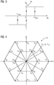
- a hysteresis interval between a negative interval limit -U Hyst and a positive interval limit + U Hyst is specified for the voltage difference ⁇ U.
- the hysteresis is defined for the midpoint voltage U m a hysteresis width U Hyst, which is symmetrical about the half of the intermediate circuit voltage U Z around. If the If the voltage difference ⁇ U is greater than the positive interval limit + U Hyst (and thus the midpoint voltage U m is greater than (U Z + U Hyst ) / 2), the hysteresis signal S is set to the value +1.
- the hysteresis signal S is set to the value -1. If the voltage difference ⁇ U exceeds or falls below the value 0, the hysteresis signal S is set to the value 0 in each case. The hysteresis signal S remains unchanged between the value 0 and the positive interval limit + U Hyst and between the value 0 and the negative interval limit -U Hyst .
- FIG. 4 shows a space vector diagram 41 according to FIG Figures 1 and 2 executed three-level inverter 1 in a stator-fixed coordinate system with coordinates a, ⁇ .
- the space vector diagram 41 has 27 space vectors U 0 to U 26 .
- Each space vector U 0 to U 26 represents a switching state of the three-level inverter 1 in a known manner, which results from the phase switching states of the switches S U , S V , S W of the three phases U, V, W.
- a switching state of the three-level inverter 1 is denoted below by a 3-tuple (a, b, c), where a denotes the phase-switched state of the first switch S U , b denotes the phase-switched state of the second switch S V and c denotes the phase-switched state of the third switch S W denotes.
- A, b, c each take on one of the values 1, 0, -1, where the value 1 stands for the first phase switching state of the respective switch S U , S V , S W , the value 0 for the second phase switching state of the respective switch S U , S V , S W stands and the value -1 stands for the third phase switching state of the respective switch S U , S V , S W stands.
- the space vector U 8 represents the switching state (1,0, -1), which is shown in FIG 1 is shown.
- the space vectors U 0 , U 7 and U 14 are the so-called zero-voltage space vectors, which each represent a switching state in which all three switches S U , S V , S W have the same phase state.
- the space vector U 0 represents the switching state (0,0,0)
- the space vector U 7 represents the switching state (1,1,1)
- the space vector U 14 represents the switching state (-1, -1, -1).
- the zero-voltage space vectors are represented by the coordinate origin of the space vector diagram 41.
- the zero-voltage space vectors form an example of so-called redundant space vectors U 0 , U 7 , U 14 to U 26 , which coincide in the space vector diagram 41.
- the switching states represented by two redundant space vectors U 0 , U 7 , U 14 to U 26 are different, but generate (at least approximately) the same differences between the individual phase voltages and are therefore represented by space vectors U 0 , U 7 , U 14 that coincide in space vector diagram 41 to U 26 . Since the switching states of two redundant space vectors U 0 , U 7 , U 14 to U 26 generate (at least approximately) the same differences between the individual phase voltages, they also have (at least approximately) the same effect on an AC voltage side connected to the three-level inverter 1 Load.
- the space vector pairs (U 15 , U 21 ), (U 16 , U 22 ), (U 17 , U 23 ), (U 18 , U 24 ), (U 19 , U 25 ) and (U 20 , U 26 ) a pair of redundant space vectors U 15 to U 26 .
- phase currents i U , i V , i W are controlled with the current control unit 37 with a direct hysteresis current control based on several space vectors U 0 to U 26 forming a space vector group. Which space vector group is selected for regulating the phase currents i U , i V , i W depends on the actual values of the phase currents i U , i V , i W and on the hysteresis signal S as well as on the nominal output voltage of the three-level inverter 1.
- the midpoint voltage U m is also regulated, so that the midpoint voltage U m is defined by the hysteresis diagram 39 Hysteresis window for the midpoint voltage U m is returned when it leaves it.
- a different space vector group than the previously used space vector group from mutually redundant space vector groups is selected to control the phase currents i U , i V , i W in order to return the midpoint voltage U m to the hysteresis window.
- Space vector groups that are redundant to one another are referred to here as space vector groups which differ from one another only in terms of different redundant space vectors U 0 , U 7 , U 14 to U 26 .
- the regulation takes advantage of the fact that two redundant space vectors U 0 , U 7 , U 14 to U 26 represent switching states that generate (at least approximately) the same differences between the individual phase voltages, but have different effects on the midpoint voltage U m , so that the Midpoint voltage U m can be changed by changing from a space vector group previously used for regulation to a space vector group redundant for this purpose.
- that one of these criteria is preferably used which optimizes the system formed by the three-level inverter 1 and a load connected to it.
- phase currents i U , i V , i W and the midpoint voltage U m in more detail, it is assumed in the following that a space vector group is used to regulate the phase currents i U , i V , i W , which four of the space vectors U 0 to U 26 are formed, which span a rhombus in the space vector diagram 41.
- This formation of the space vector groups is used in the SDHC current control, which according to the invention is preferably used for hysteresis current control of the phase currents i U , i V , i W.
- Such a rhombus is spanned, for example, by the four space vectors U 16 , U 23 , U 3 and U 9 , which form the space vector group (U 6 , U 23 , U 3 , U 9 ).
- the space vector groups (U 22 , U 23 , U 3 , U 9 ), (U 16 , U 17 , U 3 , U 9 ) and (U 22 , U 17 , U 3 , U 9 ) are redundant for this space vector group.
- the following table shows the switching states that are represented by the space vectors U 16 , U 22 , U 17 , U 23 , U 3 , U 9 of these mutually redundant space vector groups, and a midpoint current that flows from these switching states to the midpoint 13 of the intermediate circuit 3 is directed:
- the transition from space vector U 16 to space vector U 23 requires a change in the switching state in phase U from 1 to -1 and thus a change in the phase voltage of the phase U by the full intermediate circuit voltage U Z.
- the space vector group (U 16 , U 23 , U 3 , U 9 ) therefore does not meet the above-mentioned criterion (ii).
- the transition from the space vector U 16 to the space vector U 23 requires a switchover of all three phases U, V, W. Therefore, the space vector group (U 16 , U 23 , U 3 , U 9 ) does not meet the above-mentioned criterion (iv ).
- the space vector group (U 16 , U 23 , U 3 , U 9 ) is therefore preferably not used for control.
- the transitions between the space vectors U 22 , U 23 , U 3 , U 9 only require a total of four switching operations when going around the diamond. None of these transitions requires a phase voltage to be changed by the full intermediate circuit voltage U Z. Furthermore, all of the switching states represented by the space vectors U 22 , U 23 , U 3 , U 9 in phase W match.
- the space vector group (U 22 , U 23 , U 3 , U 9 ) is therefore preferably used for regulation.
- the transitions between the space vectors U 16 , U 17 , U 3 , U 9 require a total of six switching operations when rotating around the diamond. None of these transitions requires a phase voltage to be changed by the full intermediate circuit voltage U Z. Furthermore, all of the switching states represented by the space vectors U 16 , U 17 , U 3 , U 9 in phase V correspond.
- the space vector group (U 16 , U 17 , U 3 , U 9 ) is therefore also preferably used for regulation.
- the transitions between the space vectors U 22 , U 17 , U 3 , U 9 also require a total of six switching operations when rotating around the diamond, whereby none of these transitions require a change a phase voltage around the full intermediate circuit voltage U Z requires.
- the switching states represented by the space vectors U 22 , U 17 , U 3 , U 9 do not all agree in any phase U, V, W.
- the space vector group (U 22 , U 17 , U 3 , U 9 ) is therefore preferably not used for regulation.
- the space vector group (U 22 , U 23 , U 3 , U 9 ) or the space vector group (U 16 , U 17 , U 3 , U 9 ) is therefore preferably selected for regulating the phase currents i U , i V , i W if the Regulation takes place in the diamond corresponding to these space vector groups.
- that space vector group (U 22 , U 23 , U 3 , U 9 ) or (U 16 , U 17 , U 3 , U 9 ) is selected that best meets the respective requirements, for example the switching frequency or the zero system Fulfills.
- the phase currents i U , i V , i W are controlled with the hysteresis current control used, for example with the SDHC current control, independently of the hysteresis signal S using the selected space vector group.
- the midpoint voltage U m is not regulated, but results from the hysteresis current regulation of the phase currents i U , i V , i W.
- the space vector group previously used to regulate the phase currents i U , i V , i W is replaced by one of the space vector groups (U 16 , U 23 , U 3 , U 9 ) that are redundant for this space vector group. , (U 22 , U 23 , U 3 , U 9 ), (U 16 , U 17 , U 3 , U 9 ), (U 22 , U 17 , U 3 , U 9 ) to get the midpoint voltage U m in the hysteresis window for the midpoint voltage U m .
- the previously used space vector group is preferably replaced by one of the two preferred space vector groups (U 22 , U 23 , U 3 , U 9 ), (U 16 , U 17 , U 3 , U 9 ), provided that this results in the midpoint voltage U m in the Hysteresis window can be traced back.
- phase currents i U , i V , i W and the midpoint voltage U m in other areas of the space vector diagram 41 are regulated using redundant space vector groups which form a rhombus in the respective area of the space vector diagram 41.
Landscapes
- Engineering & Computer Science (AREA)
- Power Engineering (AREA)
- Inverter Devices (AREA)
Claims (7)
- Procédé de réglage d'un onduleur (1) triphasé à trois niveaux, dans lequel- on règle des courants (iu, iv, iw) de phase de l'onduleur (1) à trois niveau par un réglage direct de courant d'hystérésis à l'aide de plusieurs vecteurs (U0 à U26) d'espace formant un groupe de vecteurs d'espace, et- on règle une tension (Um) de point médian d'un circuit (3) intermédiaire du côté de la tension continue de l'onduleur (1) à trois niveaux, en choisissant, en fonction de la tension (Um) de point médian, le groupe de vecteurs d'espace utilisé pour régler les courants (iu, iv, iw) de phase parmi plusieurs groupes de vecteurs d'espace redondants,- caractérisé en ce quepour réguler la tension (Um) de point médian, on prescrit une fenêtre d'hystérésis pour la tension (Um) de point médian et, si la tension (Um) de point médian quitte la fenêtre d'hystérésis, on choisit, pour régler les courants (iu, iv, iw) de phase, parmi les groupes de vecteurs d'espace redondants entre eux, un groupe de vecteurs d'espace autre qu'un groupe de vecteurs d'espace utilisé jusqu'ici, afin de ramener la tension (Um) de point médian dans la fenêtre d'hystérésis.
- Procédé suivant l'une des revendications précédentes, caractérisé en ce que l'on choisit le groupe de vecteurs d'espace utilisé pour le réglage en fonction d'un nombre de manipulations de commutation, qui sont nécessaires pour modifier les tensions de phase de l'onduleur (1) à trois niveaux pour des transitions entre les vecteurs d'espace (U0 à U26).
- Procédé suivant l'une des revendications précédentes, caractérisé en que l'on choisit le groupe de vecteurs d'espace utilisé pour le réglage de manière à ce que, pour des transitions entre les vecteurs d'espace (U0 à U26), le groupe de vecteurs d'espace ne nécessite pas une modification, d'une tension (Uz) de circuit intermédiaire complète du circuit (3) intermédiaire, d'une tension de phase de l'onduleur (1) à trois niveaux.
- Procédé suivant l'une des revendications précédentes, caractérisé en ce que l'on choisit le groupe de vecteurs d'espace utilisé pour le réglage de manière à ce que tous les états de commutation représentés par les vecteurs d'espace (U0 à U26) du groupe de vecteurs d'espace coïncident dans une phase (U, V, W) de l'onduleur (1) à trois niveaux.
- Procédé suivant l'une des revendications précédentes, caractérisé en ce que l'on choisit le groupe de vecteurs d'espace utilisé pour le réglage en fonction d'une marche souhaitée du système homopolaire.
- Procédé suivant l'une des revendications précédentes, caractérisé en ce que l'on utilise un réglage de courant SDHC, comme réglage de courant d'hystérésis.
- Montage (19) de réglage pour régler un onduleur (1) triphasé à trois niveaux, le montage (19) de réglage comprenant- un montage (31) de mesure de la tension, conçu pour détecter une tension (Um) de point médian de l'onduleur (1) à trois niveaux,- un montage (29) de mesure du courant, conçu pour détecter des courants (iu, iv, iw) de phase de l'onduleur (1) à trois niveaux, et- un régleur (33) d'hystérésis ayant une unité (37) de réglage du courant pour le réglage direct du courant d'hystérésis des courants (iu, iv, iw) de phase à l'aide de plusieurs vecteurs d'espace (U0 à U26) formant un groupe de vecteurs d'espace, l'unité (37) de réglage de courant étant conçue pour choisir le groupe de vecteurs d'espace en fonction des courants (iu, iv, iw) de phase détectés et de la tension (Um) de point médian détectée,caractérisé en ce que
le régleur (33) d'hystérésis a un organe (35) d'hystérésis de production d'un signal (S) d'hystérésis pour la tension (Um) de point médian détectée, le signal (S) d'hystérésis signalant si la tension (Um) de point médian détectée quitte une fenêtre d'hystérésis donnée à l'avance pour la tension (Um) de point médian, et l'unité (37) de réglage de courant étant conçue pour choisir, pour régler les courants (iu, iv, iw) de phase, parmi des groupes de vecteurs d'espace redondants entre eux, un groupe de vecteurs d'espace qu'un groupe de vecteurs d'espace utilisé jusqu'ici, afin de ramener la tension (Um) de point médian dans la fenêtre d'hystérésis, si la tension (Um) de point médian quitte la fenêtre d'hystérésis.
Priority Applications (1)
| Application Number | Priority Date | Filing Date | Title |
|---|---|---|---|
| EP16190787.8A EP3300242B1 (fr) | 2016-09-27 | 2016-09-27 | Réglage d'un onduleur à trois niveaux |
Applications Claiming Priority (1)
| Application Number | Priority Date | Filing Date | Title |
|---|---|---|---|
| EP16190787.8A EP3300242B1 (fr) | 2016-09-27 | 2016-09-27 | Réglage d'un onduleur à trois niveaux |
Publications (2)
| Publication Number | Publication Date |
|---|---|
| EP3300242A1 EP3300242A1 (fr) | 2018-03-28 |
| EP3300242B1 true EP3300242B1 (fr) | 2020-10-28 |
Family
ID=57144761
Family Applications (1)
| Application Number | Title | Priority Date | Filing Date |
|---|---|---|---|
| EP16190787.8A Active EP3300242B1 (fr) | 2016-09-27 | 2016-09-27 | Réglage d'un onduleur à trois niveaux |
Country Status (1)
| Country | Link |
|---|---|
| EP (1) | EP3300242B1 (fr) |
Families Citing this family (1)
| Publication number | Priority date | Publication date | Assignee | Title |
|---|---|---|---|---|
| EP3576284A1 (fr) | 2018-05-30 | 2019-12-04 | Siemens Aktiengesellschaft | Couplage électrique d'un premier réseau électrique avec un second réseau électrique |
-
2016
- 2016-09-27 EP EP16190787.8A patent/EP3300242B1/fr active Active
Non-Patent Citations (1)
| Title |
|---|
| None * |
Also Published As
| Publication number | Publication date |
|---|---|
| EP3300242A1 (fr) | 2018-03-28 |
Similar Documents
| Publication | Publication Date | Title |
|---|---|---|
| DE69218580T2 (de) | Steuervorrichtung eines Stromrichters | |
| DE69008315T2 (de) | Verfahren zur Steuerung eines Wechselrichters. | |
| EP2831989B1 (fr) | Circuit redresseur à injection de courant | |
| DE112008001796B4 (de) | Wechselrichtersystem und Steuerverfahren | |
| DE69210955T2 (de) | Elektrischer Leistungswandler | |
| EP3245727B1 (fr) | Module convertisseur pour convertisseur d'énergie multiniveaux | |
| DE3852330T2 (de) | Pulsbreitenmodulierter Leistungskonverter. | |
| EP2144360B1 (fr) | Procédé de fonctionnement d'un convertisseur de courant et dispositif correspondant | |
| DE102018124998B4 (de) | Leistungselektronischer Umrichter und Verfahren zum Steuern desselben | |
| EP3504781B1 (fr) | Réglage hysterese d'un courant de sortie d'un convertisseur | |
| DE102020108035B3 (de) | Modularer Multilevel-Umrichter, Verfahren zum Betrieb von modularen Multilevel-Umrichtern und Computerprogramm | |
| EP2992595A1 (fr) | Ensemble mutateur à mutateurs multi-étages câblés en parallèle et son procédé de commande | |
| EP2697901B1 (fr) | Dispositif de réglage de tension | |
| EP0743744B1 (fr) | Convertisseur de courant | |
| EP3476035B1 (fr) | Régulation de courants de phases d'un onduleur | |
| AT516643B1 (de) | Gleichrichterschaltung | |
| EP3300242B1 (fr) | Réglage d'un onduleur à trois niveaux | |
| WO2013023914A1 (fr) | Dispositif onduleur | |
| EP3482488B1 (fr) | Reglage des courants de phase d'onduleurs couples en parallele | |
| WO2017050960A1 (fr) | Procédé de fonctionnement d'un convertisseur de courant modulaire à multiples niveaux, convertisseur de courant modulaire à multiples niveaux ainsi que programme d'ordinateur | |
| AT514654A1 (de) | Gleichrichterschaltung mit Strominjektion | |
| DE112021008196T5 (de) | Steuerungseinheit für einen stromrichter, sowie stromrichtervorrichtung | |
| DE112021008195T5 (de) | Stromrichtereinrichtung | |
| EP3556003B1 (fr) | Convertisseur multi-niveaux et procédé de fonctionnement | |
| DE112015000929T5 (de) | Einrichtung und Verfahren zum Reduzieren von Oberschwingungen |
Legal Events
| Date | Code | Title | Description |
|---|---|---|---|
| PUAI | Public reference made under article 153(3) epc to a published international application that has entered the european phase |
Free format text: ORIGINAL CODE: 0009012 |
|
| STAA | Information on the status of an ep patent application or granted ep patent |
Free format text: STATUS: THE APPLICATION HAS BEEN PUBLISHED |
|
| AK | Designated contracting states |
Kind code of ref document: A1 Designated state(s): AL AT BE BG CH CY CZ DE DK EE ES FI FR GB GR HR HU IE IS IT LI LT LU LV MC MK MT NL NO PL PT RO RS SE SI SK SM TR |
|
| AX | Request for extension of the european patent |
Extension state: BA ME |
|
| STAA | Information on the status of an ep patent application or granted ep patent |
Free format text: STATUS: REQUEST FOR EXAMINATION WAS MADE |
|
| 17P | Request for examination filed |
Effective date: 20180920 |
|
| RBV | Designated contracting states (corrected) |
Designated state(s): AL AT BE BG CH CY CZ DE DK EE ES FI FR GB GR HR HU IE IS IT LI LT LU LV MC MK MT NL NO PL PT RO RS SE SI SK SM TR |
|
| GRAP | Despatch of communication of intention to grant a patent |
Free format text: ORIGINAL CODE: EPIDOSNIGR1 |
|
| STAA | Information on the status of an ep patent application or granted ep patent |
Free format text: STATUS: GRANT OF PATENT IS INTENDED |
|
| INTG | Intention to grant announced |
Effective date: 20200622 |
|
| GRAS | Grant fee paid |
Free format text: ORIGINAL CODE: EPIDOSNIGR3 |
|
| GRAA | (expected) grant |
Free format text: ORIGINAL CODE: 0009210 |
|
| STAA | Information on the status of an ep patent application or granted ep patent |
Free format text: STATUS: THE PATENT HAS BEEN GRANTED |
|
| AK | Designated contracting states |
Kind code of ref document: B1 Designated state(s): AL AT BE BG CH CY CZ DE DK EE ES FI FR GB GR HR HU IE IS IT LI LT LU LV MC MK MT NL NO PL PT RO RS SE SI SK SM TR |
|
| REG | Reference to a national code |
Ref country code: GB Ref legal event code: FG4D Free format text: NOT ENGLISH |
|
| REG | Reference to a national code |
Ref country code: CH Ref legal event code: EP |
|
| REG | Reference to a national code |
Ref country code: DE Ref legal event code: R096 Ref document number: 502016011537 Country of ref document: DE |
|
| REG | Reference to a national code |
Ref country code: AT Ref legal event code: REF Ref document number: 1329242 Country of ref document: AT Kind code of ref document: T Effective date: 20201115 |
|
| REG | Reference to a national code |
Ref country code: IE Ref legal event code: FG4D Free format text: LANGUAGE OF EP DOCUMENT: GERMAN |
|
| REG | Reference to a national code |
Ref country code: NL Ref legal event code: MP Effective date: 20201028 |
|
| PG25 | Lapsed in a contracting state [announced via postgrant information from national office to epo] |
Ref country code: NO Free format text: LAPSE BECAUSE OF FAILURE TO SUBMIT A TRANSLATION OF THE DESCRIPTION OR TO PAY THE FEE WITHIN THE PRESCRIBED TIME-LIMIT Effective date: 20210128 Ref country code: RS Free format text: LAPSE BECAUSE OF FAILURE TO SUBMIT A TRANSLATION OF THE DESCRIPTION OR TO PAY THE FEE WITHIN THE PRESCRIBED TIME-LIMIT Effective date: 20201028 Ref country code: PT Free format text: LAPSE BECAUSE OF FAILURE TO SUBMIT A TRANSLATION OF THE DESCRIPTION OR TO PAY THE FEE WITHIN THE PRESCRIBED TIME-LIMIT Effective date: 20210301 Ref country code: GR Free format text: LAPSE BECAUSE OF FAILURE TO SUBMIT A TRANSLATION OF THE DESCRIPTION OR TO PAY THE FEE WITHIN THE PRESCRIBED TIME-LIMIT Effective date: 20210129 Ref country code: FI Free format text: LAPSE BECAUSE OF FAILURE TO SUBMIT A TRANSLATION OF THE DESCRIPTION OR TO PAY THE FEE WITHIN THE PRESCRIBED TIME-LIMIT Effective date: 20201028 |
|
| REG | Reference to a national code |
Ref country code: LT Ref legal event code: MG4D |
|
| PG25 | Lapsed in a contracting state [announced via postgrant information from national office to epo] |
Ref country code: SE Free format text: LAPSE BECAUSE OF FAILURE TO SUBMIT A TRANSLATION OF THE DESCRIPTION OR TO PAY THE FEE WITHIN THE PRESCRIBED TIME-LIMIT Effective date: 20201028 Ref country code: ES Free format text: LAPSE BECAUSE OF FAILURE TO SUBMIT A TRANSLATION OF THE DESCRIPTION OR TO PAY THE FEE WITHIN THE PRESCRIBED TIME-LIMIT Effective date: 20201028 Ref country code: PL Free format text: LAPSE BECAUSE OF FAILURE TO SUBMIT A TRANSLATION OF THE DESCRIPTION OR TO PAY THE FEE WITHIN THE PRESCRIBED TIME-LIMIT Effective date: 20201028 Ref country code: LV Free format text: LAPSE BECAUSE OF FAILURE TO SUBMIT A TRANSLATION OF THE DESCRIPTION OR TO PAY THE FEE WITHIN THE PRESCRIBED TIME-LIMIT Effective date: 20201028 Ref country code: IS Free format text: LAPSE BECAUSE OF FAILURE TO SUBMIT A TRANSLATION OF THE DESCRIPTION OR TO PAY THE FEE WITHIN THE PRESCRIBED TIME-LIMIT Effective date: 20210228 Ref country code: BG Free format text: LAPSE BECAUSE OF FAILURE TO SUBMIT A TRANSLATION OF THE DESCRIPTION OR TO PAY THE FEE WITHIN THE PRESCRIBED TIME-LIMIT Effective date: 20210128 |
|
| PG25 | Lapsed in a contracting state [announced via postgrant information from national office to epo] |
Ref country code: HR Free format text: LAPSE BECAUSE OF FAILURE TO SUBMIT A TRANSLATION OF THE DESCRIPTION OR TO PAY THE FEE WITHIN THE PRESCRIBED TIME-LIMIT Effective date: 20201028 Ref country code: NL Free format text: LAPSE BECAUSE OF FAILURE TO SUBMIT A TRANSLATION OF THE DESCRIPTION OR TO PAY THE FEE WITHIN THE PRESCRIBED TIME-LIMIT Effective date: 20201028 |
|
| REG | Reference to a national code |
Ref country code: DE Ref legal event code: R097 Ref document number: 502016011537 Country of ref document: DE |
|
| PG25 | Lapsed in a contracting state [announced via postgrant information from national office to epo] |
Ref country code: SK Free format text: LAPSE BECAUSE OF FAILURE TO SUBMIT A TRANSLATION OF THE DESCRIPTION OR TO PAY THE FEE WITHIN THE PRESCRIBED TIME-LIMIT Effective date: 20201028 Ref country code: RO Free format text: LAPSE BECAUSE OF FAILURE TO SUBMIT A TRANSLATION OF THE DESCRIPTION OR TO PAY THE FEE WITHIN THE PRESCRIBED TIME-LIMIT Effective date: 20201028 Ref country code: LT Free format text: LAPSE BECAUSE OF FAILURE TO SUBMIT A TRANSLATION OF THE DESCRIPTION OR TO PAY THE FEE WITHIN THE PRESCRIBED TIME-LIMIT Effective date: 20201028 Ref country code: SM Free format text: LAPSE BECAUSE OF FAILURE TO SUBMIT A TRANSLATION OF THE DESCRIPTION OR TO PAY THE FEE WITHIN THE PRESCRIBED TIME-LIMIT Effective date: 20201028 Ref country code: EE Free format text: LAPSE BECAUSE OF FAILURE TO SUBMIT A TRANSLATION OF THE DESCRIPTION OR TO PAY THE FEE WITHIN THE PRESCRIBED TIME-LIMIT Effective date: 20201028 Ref country code: CZ Free format text: LAPSE BECAUSE OF FAILURE TO SUBMIT A TRANSLATION OF THE DESCRIPTION OR TO PAY THE FEE WITHIN THE PRESCRIBED TIME-LIMIT Effective date: 20201028 |
|
| PG25 | Lapsed in a contracting state [announced via postgrant information from national office to epo] |
Ref country code: DK Free format text: LAPSE BECAUSE OF FAILURE TO SUBMIT A TRANSLATION OF THE DESCRIPTION OR TO PAY THE FEE WITHIN THE PRESCRIBED TIME-LIMIT Effective date: 20201028 |
|
| PLBE | No opposition filed within time limit |
Free format text: ORIGINAL CODE: 0009261 |
|
| STAA | Information on the status of an ep patent application or granted ep patent |
Free format text: STATUS: NO OPPOSITION FILED WITHIN TIME LIMIT |
|
| 26N | No opposition filed |
Effective date: 20210729 |
|
| PG25 | Lapsed in a contracting state [announced via postgrant information from national office to epo] |
Ref country code: AL Free format text: LAPSE BECAUSE OF FAILURE TO SUBMIT A TRANSLATION OF THE DESCRIPTION OR TO PAY THE FEE WITHIN THE PRESCRIBED TIME-LIMIT Effective date: 20201028 |
|
| PG25 | Lapsed in a contracting state [announced via postgrant information from national office to epo] |
Ref country code: SI Free format text: LAPSE BECAUSE OF FAILURE TO SUBMIT A TRANSLATION OF THE DESCRIPTION OR TO PAY THE FEE WITHIN THE PRESCRIBED TIME-LIMIT Effective date: 20201028 |
|
| REG | Reference to a national code |
Ref country code: CH Ref legal event code: PL |
|
| REG | Reference to a national code |
Ref country code: BE Ref legal event code: MM Effective date: 20210930 |
|
| GBPC | Gb: european patent ceased through non-payment of renewal fee |
Effective date: 20210927 |
|
| PG25 | Lapsed in a contracting state [announced via postgrant information from national office to epo] |
Ref country code: IS Free format text: LAPSE BECAUSE OF FAILURE TO SUBMIT A TRANSLATION OF THE DESCRIPTION OR TO PAY THE FEE WITHIN THE PRESCRIBED TIME-LIMIT Effective date: 20210228 Ref country code: MC Free format text: LAPSE BECAUSE OF FAILURE TO SUBMIT A TRANSLATION OF THE DESCRIPTION OR TO PAY THE FEE WITHIN THE PRESCRIBED TIME-LIMIT Effective date: 20201028 |
|
| PG25 | Lapsed in a contracting state [announced via postgrant information from national office to epo] |
Ref country code: LU Free format text: LAPSE BECAUSE OF NON-PAYMENT OF DUE FEES Effective date: 20210927 Ref country code: IE Free format text: LAPSE BECAUSE OF NON-PAYMENT OF DUE FEES Effective date: 20210927 Ref country code: GB Free format text: LAPSE BECAUSE OF NON-PAYMENT OF DUE FEES Effective date: 20210927 Ref country code: BE Free format text: LAPSE BECAUSE OF NON-PAYMENT OF DUE FEES Effective date: 20210930 |
|
| PG25 | Lapsed in a contracting state [announced via postgrant information from national office to epo] |
Ref country code: LI Free format text: LAPSE BECAUSE OF NON-PAYMENT OF DUE FEES Effective date: 20210930 Ref country code: CH Free format text: LAPSE BECAUSE OF NON-PAYMENT OF DUE FEES Effective date: 20210930 |
|
| REG | Reference to a national code |
Ref country code: AT Ref legal event code: MM01 Ref document number: 1329242 Country of ref document: AT Kind code of ref document: T Effective date: 20210927 |
|
| PG25 | Lapsed in a contracting state [announced via postgrant information from national office to epo] |
Ref country code: AT Free format text: LAPSE BECAUSE OF NON-PAYMENT OF DUE FEES Effective date: 20210927 |
|
| PG25 | Lapsed in a contracting state [announced via postgrant information from national office to epo] |
Ref country code: HU Free format text: LAPSE BECAUSE OF FAILURE TO SUBMIT A TRANSLATION OF THE DESCRIPTION OR TO PAY THE FEE WITHIN THE PRESCRIBED TIME-LIMIT; INVALID AB INITIO Effective date: 20160927 |
|
| PG25 | Lapsed in a contracting state [announced via postgrant information from national office to epo] |
Ref country code: CY Free format text: LAPSE BECAUSE OF FAILURE TO SUBMIT A TRANSLATION OF THE DESCRIPTION OR TO PAY THE FEE WITHIN THE PRESCRIBED TIME-LIMIT Effective date: 20201028 |
|
| PG25 | Lapsed in a contracting state [announced via postgrant information from national office to epo] |
Ref country code: MK Free format text: LAPSE BECAUSE OF FAILURE TO SUBMIT A TRANSLATION OF THE DESCRIPTION OR TO PAY THE FEE WITHIN THE PRESCRIBED TIME-LIMIT Effective date: 20201028 |
|
| PG25 | Lapsed in a contracting state [announced via postgrant information from national office to epo] |
Ref country code: TR Free format text: LAPSE BECAUSE OF FAILURE TO SUBMIT A TRANSLATION OF THE DESCRIPTION OR TO PAY THE FEE WITHIN THE PRESCRIBED TIME-LIMIT Effective date: 20201028 |
|
| PG25 | Lapsed in a contracting state [announced via postgrant information from national office to epo] |
Ref country code: MT Free format text: LAPSE BECAUSE OF FAILURE TO SUBMIT A TRANSLATION OF THE DESCRIPTION OR TO PAY THE FEE WITHIN THE PRESCRIBED TIME-LIMIT Effective date: 20201028 |
|
| PGFP | Annual fee paid to national office [announced via postgrant information from national office to epo] |
Ref country code: IT Payment date: 20250924 Year of fee payment: 10 |
|
| PGFP | Annual fee paid to national office [announced via postgrant information from national office to epo] |
Ref country code: FR Payment date: 20250915 Year of fee payment: 10 |
|
| PGFP | Annual fee paid to national office [announced via postgrant information from national office to epo] |
Ref country code: DE Payment date: 20251120 Year of fee payment: 10 |