EP2146373A2 - Agencement doté d'un module semi-conducteur de puissance et son procédé de fabrication - Google Patents
Agencement doté d'un module semi-conducteur de puissance et son procédé de fabrication Download PDFInfo
- Publication number
- EP2146373A2 EP2146373A2 EP09008704A EP09008704A EP2146373A2 EP 2146373 A2 EP2146373 A2 EP 2146373A2 EP 09008704 A EP09008704 A EP 09008704A EP 09008704 A EP09008704 A EP 09008704A EP 2146373 A2 EP2146373 A2 EP 2146373A2
- Authority
- EP
- European Patent Office
- Prior art keywords
- housing
- recess
- heat sink
- substrate
- arrangement according
- Prior art date
- Legal status (The legal status is an assumption and is not a legal conclusion. Google has not performed a legal analysis and makes no representation as to the accuracy of the status listed.)
- Withdrawn
Links
Images



Classifications
-
- H—ELECTRICITY
- H10—SEMICONDUCTOR DEVICES; ELECTRIC SOLID-STATE DEVICES NOT OTHERWISE PROVIDED FOR
- H10W—GENERIC PACKAGES, INTERCONNECTIONS, CONNECTORS OR OTHER CONSTRUCTIONAL DETAILS OF DEVICES COVERED BY CLASS H10
- H10W40/00—Arrangements for thermal protection or thermal control
- H10W40/10—Arrangements for heating
-
- H—ELECTRICITY
- H10—SEMICONDUCTOR DEVICES; ELECTRIC SOLID-STATE DEVICES NOT OTHERWISE PROVIDED FOR
- H10W—GENERIC PACKAGES, INTERCONNECTIONS, CONNECTORS OR OTHER CONSTRUCTIONAL DETAILS OF DEVICES COVERED BY CLASS H10
- H10W76/00—Containers; Fillings or auxiliary members therefor; Seals
- H10W76/60—Seals
-
- H—ELECTRICITY
- H10—SEMICONDUCTOR DEVICES; ELECTRIC SOLID-STATE DEVICES NOT OTHERWISE PROVIDED FOR
- H10W—GENERIC PACKAGES, INTERCONNECTIONS, CONNECTORS OR OTHER CONSTRUCTIONAL DETAILS OF DEVICES COVERED BY CLASS H10
- H10W40/00—Arrangements for thermal protection or thermal control
- H10W40/60—Securing means for detachable heating or cooling arrangements, e.g. clamps
- H10W40/641—Snap-on arrangements, e.g. clips
-
- H—ELECTRICITY
- H10—SEMICONDUCTOR DEVICES; ELECTRIC SOLID-STATE DEVICES NOT OTHERWISE PROVIDED FOR
- H10W—GENERIC PACKAGES, INTERCONNECTIONS, CONNECTORS OR OTHER CONSTRUCTIONAL DETAILS OF DEVICES COVERED BY CLASS H10
- H10W76/00—Containers; Fillings or auxiliary members therefor; Seals
- H10W76/10—Containers or parts thereof
- H10W76/12—Containers or parts thereof characterised by their shape
- H10W76/15—Containers comprising an insulating or insulated base
-
- H—ELECTRICITY
- H10—SEMICONDUCTOR DEVICES; ELECTRIC SOLID-STATE DEVICES NOT OTHERWISE PROVIDED FOR
- H10W—GENERIC PACKAGES, INTERCONNECTIONS, CONNECTORS OR OTHER CONSTRUCTIONAL DETAILS OF DEVICES COVERED BY CLASS H10
- H10W90/00—Package configurations
-
- H—ELECTRICITY
- H10—SEMICONDUCTOR DEVICES; ELECTRIC SOLID-STATE DEVICES NOT OTHERWISE PROVIDED FOR
- H10W—GENERIC PACKAGES, INTERCONNECTIONS, CONNECTORS OR OTHER CONSTRUCTIONAL DETAILS OF DEVICES COVERED BY CLASS H10
- H10W40/00—Arrangements for thermal protection or thermal control
- H10W40/20—Arrangements for cooling
- H10W40/25—Arrangements for cooling characterised by their materials
- H10W40/255—Arrangements for cooling characterised by their materials having a laminate or multilayered structure, e.g. direct bond copper [DBC] ceramic substrates
-
- H—ELECTRICITY
- H10—SEMICONDUCTOR DEVICES; ELECTRIC SOLID-STATE DEVICES NOT OTHERWISE PROVIDED FOR
- H10W—GENERIC PACKAGES, INTERCONNECTIONS, CONNECTORS OR OTHER CONSTRUCTIONAL DETAILS OF DEVICES COVERED BY CLASS H10
- H10W76/00—Containers; Fillings or auxiliary members therefor; Seals
- H10W76/10—Containers or parts thereof
- H10W76/17—Containers or parts thereof characterised by their materials
Definitions
- the invention relates to an arrangement having a power semiconductor module, comprising a substrate having at least one power semiconductor element and a housing, and a heat sink for dissipating waste heat of the at least one power semiconductor element, wherein the housing has a recess arranged on a lower side of the housing facing the heat sink for receiving the substrate having.
- the invention further relates to a method for producing such an arrangement.
- Arrangements of the type mentioned are for example from the DE 101 49 886 A1 known. It describes a baseplate-free power semiconductor module in which the underside of the substrate is pressed by a contact pressure device onto a heat sink, via which heat losses occurring during the operation of the power semiconductor module are dissipated.
- the underside of the substrate with a
- the underside of the substrate can be printed with a thermal compound.
- Such coated baseplateless power semiconductor modules are very sensitive to disassembly from the heat sink.
- the substrate When disassembling the substrate, the substrate can be released from the housing due to the high adhesive forces of the thermal compound.
- the object is for the arrangement with a power semiconductor module, comprising a substrate having at least one power semiconductor element and a housing, and a heat sink for dissipating waste heat of the at least one power semiconductor element, wherein the housing arranged on a side facing the heat sink bottom of the housing recess for receiving the Substrate comprises, achieved in that the power semiconductor module has at least one holding element which engages in a recess associated with the at least one retaining element on the underside of the housing and is formed so that it limits a movement of the substrate in the direction of the underside of the housing.
- Such an arrangement has the advantage that the substrate with the power semiconductor elements can not detach from the housing during disassembly of the heat sink.
- the holding element holds the substrate during disassembly in the housing.
- the holding element makes it possible that the substrate can be detached together with the housing from the heat sink.
- the holding element is not formed on the housing or integrally formed with the housing, but formed as a separate, independent component which is mounted on the assembly of the individual elements of the assembly to the housing.
- the holding element may be formed of any material, preferably of plastic or metal.
- the at least one retaining element is formed so that it engages in the mounting of the housing on the heat sink for positioning the housing on the heat sink in an associated recess of the heat sink.
- This is a centering the housing, and thus the substrate, on the heat sink possible.
- the substrate is precentered by means of the holding element during assembly and prevents displacement of the substrate during assembly.
- the disadvantages are avoided, which arise when the housing is not pre-centered during assembly of the arrangement. Because of the lack of pre-centering, there is a risk that, during a subsequently performed positional correction of the housing on the heat sink, due to the adhesion of the thermal paste, the substrate shifts relative to the housing and protrudes under the edge of the housing, through which the substrate can then be damaged.
- the application of a heat conducting layer formed from a thermal compound on the side facing the heat sink side of the substrate takes place before the at least one holding element is introduced into the recess of the housing.
- the application of the thermal paste to the substrate in a coating or printing process is easily possible without disturbing the holding elements.
- the holding elements are introduced into the recesses provided for this purpose of the housing.
- This preferred embodiment of the method according to the invention thus avoids the disadvantages that arise when a centering element is formed, for example molded, during the manufacture of the housing on the housing, in order to enable the centering of the housing.
- a centering element is formed, for example molded, during the manufacture of the housing on the housing, in order to enable the centering of the housing.
- the molding of a centering element on the housing as practiced in previously known methods, namely the printing of a substrate, which is located in the housing, with thermal paste impossible or at least difficult.
- the holding element according to the invention can be arranged on the housing after the substrate has been coated.
- the at least one holding element associated with the recess of the heat sink and a heat sink facing portion of the holding element, which engages in said recess have a mutually corresponding shape.
- the recess of the heat sink and the engaging therein portion of the holding member are matched in shape to each other that the holding member in the recess of the heat sink can perform virtually no movement in a direction parallel to a contact plane of the heat sink and housing. In this way, the holding element allows the housing to assume a precise and predefined position on the heat sink.
- a section of the holding element facing the heat sink is cylindrical.
- a preferred form of the heat sink facing portion of the support member is a cylindrical shape with a chamfer, that is, with a chamfer of the heat sink facing edge.
- the holding member is hollow inside, e.g. along its longitudinal axis a continuous, preferably cylindrical, recess identifies.
- the at least one retaining element has a protruding into the recess for receiving the substrate projection which limits the movement of the substrate in the direction of the bottom of the housing.
- the lead on The holding element is easy to manufacture and forms a mechanically reliable holding device.
- the housing has a peripheral housing frame, in which the recess is arranged, in which engages the retaining element.
- the recess is formed on the underside of the housing as a blind hole open towards the underside of the housing into which the at least one retaining element engages from the underside of the housing.
- the at least one retaining element is designed as a latching centering holder.
- the power module is pre-centered during assembly and at the same time avoiding a displacement of the substrate during assembly.
- the substrate is held in the housing during disassembly by the latching centering holder. The substrate can thus be detached from the heat sink.
- the at least one retaining element is connected to the housing by means of a detachable connection.
- a detachable connection is designed as a screw, that is, that the holding element has an external thread and the recess of the housing has an internal thread associated with the external thread on a section engaging in the recess of the housing.
- the retaining element has at least one resilient latching finger on a section engaging in the recess of the housing and the recess of the housing has a latching recess assigned to the latching finger.
- the at least one holding element is fixed by means of an adhesive connection in the associated recess of the housing.
- the power semiconductor module comprises at least two holding elements.
- the power semiconductor module has at least three holding elements.
- the recesses associated with the at least two retaining elements are preferably arranged on the underside of the housing on opposite sides of the housing, in particular diagonally opposite one another.
- the arrangement of at least two or at least three retaining elements has the advantage that the substrate is held securely in the recess of the housing.
- the at least two or at least three holding elements allow a particularly good pre-centering of the housing in several directions on the heat sink.
- the arrangement has a heat conducting layer formed of a thermal compound between the substrate and the heat sink.
- the heat transfer of the waste heat of the power semiconductor element located on the substrate to the heat sink delivering the heat sink can be decisively improved.
- FIG. 1 shows the bottom 40 of a housing 4, which has a recess 41 for receiving two substrates 2.
- DCB Direct Copper Bonded
- mounting holes 45 can be passed through the screws with which the housing 4 on a heat sink (not shown) is mounted.
- the housing 4 has on its underside 40 a circumferential frame 43, in which recesses 42 are arranged for receiving retaining elements 5.
- FIG. 2 shows an enlarged view of the right part of in FIG. 1 illustrated housing 4.
- FIG. 3a shows a section through the in FIG. 2 shown holding element 5 along in FIG. 2 indicated section line IIIa.
- the holding element 5 engages in a recess 42 of the housing 4.
- the holding element 5 has a projection 54 which bears against the underside 40 of the housing 4.
- the projection 54 of the holding element protrudes from the peripheral frame 43 of the housing 4 in the direction of the substrate 2.
- the projection 54 serves as a stop for the substrate 2 and limits the movement of the substrate 2 in the direction of the underside 40 of the housing 4. That is, the holding element 5 fixes the substrate and secures the substrate 2 from falling out of the recess 41.
- FIG. 3b shows a section through the holding element 5 along in FIG. 2 indicated section line IIIb.
- the heat sink 3 facing portion 51 of the support member 5 has a cup-shaped outline.
- the engaging in the housing recess 42 portion 52 of the support member 5 has two latching fingers 53 which engage in corresponding locking recesses 44 of the recess 42 so that a snap-locking connection is formed.
- FIG. 4 shows a cross section through an inventive arrangement.
- the arrangement has a power semiconductor module 1, comprising a substrate 2 with two power semiconductor elements 20 and a housing 4, and a heat sink 3 for dissipating waste heat of the power semiconductor elements 20.
- the housing 4 has a recess 41, which is arranged on a lower side 40 of the housing 4 facing the heat sink 3, for receiving the substrate 2.
- the power semiconductor module 1 has two holding elements 5, which engage in the holding elements 5 associated housing recesses 42 on the underside 40 of the housing 4 and limit movement of the substrate 2 in the direction of the bottom 40 of the housing.
- Between the substrate 2 and the heat sink 3 is a heat conducting layer formed of a thermal paste 6.
- the housing recesses 42 have locking recesses 44.
- the heat sink 3 has two recesses 30, in which the holding elements 5 engage.
- the shape of the recesses 30 engaging portions 51 of the holding elements 5 is adapted to the shape of the recesses 30 of the heat sink 3, so that the housing 4 can be positioned only in a desired and defined position on the heat sink 30.
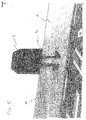
- FIG. 5 shows a section through a holding element 5, which engages in an associated recess 42 of a housing 4.
- the retaining element 5 is inserted into the recess 42 from the underside 40 of the housing 4.
- the holding element 5 has two latching fingers 53, which engage in a corresponding latching recess 44 of the recess 42.
- FIGS. 6a to 6d show different views of a holding element 5, as it has the inventive arrangement with the power semiconductor module 1.
- FIG. 6a shows an oblique view from below on the holding element 5.
- the holding member 5 has an upper portion 51 which engages in a recess 30 of the heat sink 3, and a lower portion 52 which engages in the housing recess 42 of the housing 4.
- the lower portion 52 has two resilient latching fingers 53, which form a snap-snap connection with the associated recess 42 of the housing 4.
- FIG. 6b shows a bottom view of in FIG. 6a shown holding element. 5
- FIG. 6c shows a side view of the in FIG. 6a shown holding element. 5
- FIG. 6d shows a second side view of the in FIG. 6a shown holding element. 5
Landscapes
- Cooling Or The Like Of Semiconductors Or Solid State Devices (AREA)
- Cooling Or The Like Of Electrical Apparatus (AREA)
Applications Claiming Priority (1)
| Application Number | Priority Date | Filing Date | Title |
|---|---|---|---|
| DE102008033852A DE102008033852B3 (de) | 2008-07-19 | 2008-07-19 | Anordnung mit einem Leistungshalbleitermodul und Verfahren zu deren Herstellung |
Publications (2)
| Publication Number | Publication Date |
|---|---|
| EP2146373A2 true EP2146373A2 (fr) | 2010-01-20 |
| EP2146373A3 EP2146373A3 (fr) | 2011-05-04 |
Family
ID=40936599
Family Applications (1)
| Application Number | Title | Priority Date | Filing Date |
|---|---|---|---|
| EP09008704A Withdrawn EP2146373A3 (fr) | 2008-07-19 | 2009-07-03 | Agencement doté d'un module semi-conducteur de puissance et son procédé de fabrication |
Country Status (6)
| Country | Link |
|---|---|
| US (1) | US7965516B2 (fr) |
| EP (1) | EP2146373A3 (fr) |
| JP (1) | JP5186449B2 (fr) |
| KR (1) | KR101595127B1 (fr) |
| CN (1) | CN101630663B (fr) |
| DE (1) | DE102008033852B3 (fr) |
Families Citing this family (7)
| Publication number | Priority date | Publication date | Assignee | Title |
|---|---|---|---|---|
| DE102008033852B3 (de) | 2008-07-19 | 2009-09-10 | Semikron Elektronik Gmbh & Co. Kg | Anordnung mit einem Leistungshalbleitermodul und Verfahren zu deren Herstellung |
| JP5623463B2 (ja) | 2012-06-25 | 2014-11-12 | 三菱電機株式会社 | 半導体モジュール |
| US9258878B2 (en) * | 2013-02-13 | 2016-02-09 | Gerald Ho Kim | Isolation of thermal ground for multiple heat-generating devices on a substrate |
| US10276957B2 (en) * | 2013-08-27 | 2019-04-30 | Continental Automotive Systems, Inc. | Grounding method for baseplate sealed enclosures |
| US12513870B2 (en) | 2021-07-22 | 2025-12-30 | Semiconductor Components Industries, Llc | Power module |
| CN115394732B (zh) * | 2022-05-30 | 2023-09-05 | 安世半导体科技(上海)有限公司 | 功率半导体模块及其装配方法 |
| DE102024205059A1 (de) | 2024-05-31 | 2025-12-04 | Robert Bosch Gesellschaft mit beschränkter Haftung | Elektronikanordnung mit Aufnahmebereich zur Handhabung mittels einer Handhabungsvorrichtung |
Citations (1)
| Publication number | Priority date | Publication date | Assignee | Title |
|---|---|---|---|---|
| DE10149886A1 (de) | 2001-10-10 | 2003-04-30 | Eupec Gmbh & Co Kg | Leistunghalbleitermodul |
Family Cites Families (17)
| Publication number | Priority date | Publication date | Assignee | Title |
|---|---|---|---|---|
| DE3505086A1 (de) * | 1985-02-14 | 1986-08-28 | Brown, Boveri & Cie Ag, 6800 Mannheim | Leistungshalbleitermodul mit einem kunststoffgehaeuse |
| DE3604882A1 (de) * | 1986-02-15 | 1987-08-20 | Bbc Brown Boveri & Cie | Leistungshalbleitermodul und verfahren zur herstellung des moduls |
| JP3225457B2 (ja) * | 1995-02-28 | 2001-11-05 | 株式会社日立製作所 | 半導体装置 |
| DE19530264A1 (de) * | 1995-08-17 | 1997-02-20 | Abb Management Ag | Leistungshalbleitermodul |
| DE19533298A1 (de) * | 1995-09-08 | 1997-03-13 | Siemens Ag | Elektronisches Modul mit Leistungsbauelementen |
| JPH1093016A (ja) * | 1996-09-19 | 1998-04-10 | Hitachi Ltd | パワー半導体装置 |
| JPH1187610A (ja) * | 1997-09-05 | 1999-03-30 | Mitsubishi Electric Corp | 半導体装置 |
| US6104614A (en) * | 1998-04-09 | 2000-08-15 | Hon Hai Precision Ind. Co., Ltd. | Fastening device for tight attachment between two plates |
| JP2002184921A (ja) * | 2000-12-18 | 2002-06-28 | Nissan Motor Co Ltd | 半導体装置とヒートシンクの結合構造 |
| DE10064194B4 (de) * | 2000-12-22 | 2006-12-07 | Infineon Technologies Ag | Leistungshalbleiter-Modul und Kühlkörper zur Aufnahme des Leistungshalbleiter-Moduls |
| DE10117797C2 (de) * | 2001-04-10 | 2003-04-17 | Bosch Gmbh Robert | Montagevorrichtung und Verfahren zum Aufbau eines elektronischen Bauteils |
| DE10326176A1 (de) * | 2003-06-10 | 2005-01-05 | eupec Europäische Gesellschaft für Leistungshalbleiter mbH | Leistungshalbleitermodul |
| US7477518B2 (en) * | 2004-09-06 | 2009-01-13 | Infineon Technologies Ag | Sub-assembly |
| ATE535018T1 (de) * | 2004-12-17 | 2011-12-15 | Siemens Ag | Halbleiterschaltmodul |
| JP4232770B2 (ja) * | 2005-09-22 | 2009-03-04 | 株式会社デンソー | 電子制御装置 |
| DE102006008807B4 (de) * | 2006-02-25 | 2010-10-14 | Semikron Elektronik Gmbh & Co. Kg | Anordnung mit einem Leistungshalbleitermodul und einem Kühlbauteil |
| DE102008033852B3 (de) | 2008-07-19 | 2009-09-10 | Semikron Elektronik Gmbh & Co. Kg | Anordnung mit einem Leistungshalbleitermodul und Verfahren zu deren Herstellung |
-
2008
- 2008-07-19 DE DE102008033852A patent/DE102008033852B3/de not_active Expired - Fee Related
-
2009
- 2009-07-03 EP EP09008704A patent/EP2146373A3/fr not_active Withdrawn
- 2009-07-16 KR KR1020090064891A patent/KR101595127B1/ko not_active Expired - Fee Related
- 2009-07-16 JP JP2009167693A patent/JP5186449B2/ja not_active Expired - Fee Related
- 2009-07-17 CN CN2009101399658A patent/CN101630663B/zh not_active Expired - Fee Related
- 2009-07-20 US US12/505,950 patent/US7965516B2/en not_active Expired - Fee Related
Patent Citations (1)
| Publication number | Priority date | Publication date | Assignee | Title |
|---|---|---|---|---|
| DE10149886A1 (de) | 2001-10-10 | 2003-04-30 | Eupec Gmbh & Co Kg | Leistunghalbleitermodul |
Also Published As
| Publication number | Publication date |
|---|---|
| DE102008033852B3 (de) | 2009-09-10 |
| JP2010028117A (ja) | 2010-02-04 |
| CN101630663A (zh) | 2010-01-20 |
| EP2146373A3 (fr) | 2011-05-04 |
| CN101630663B (zh) | 2013-08-14 |
| US7965516B2 (en) | 2011-06-21 |
| JP5186449B2 (ja) | 2013-04-17 |
| US20100039774A1 (en) | 2010-02-18 |
| KR101595127B1 (ko) | 2016-02-26 |
| KR20100009621A (ko) | 2010-01-28 |
Similar Documents
| Publication | Publication Date | Title |
|---|---|---|
| DE102012215705B4 (de) | Gehäuse für ein optisches bauelement, baugruppe, verfahren zum herstellen eines gehäuses und verfahren zum herstellen einer baugruppe | |
| DE68908808T2 (de) | Verfahren zum Montieren elektronischer Mikrokomponenten auf einer Unterlage und Zwischenprodukt. | |
| DE69432968T2 (de) | Gehäuse für elektronische Bauelemente | |
| DE102008033852B3 (de) | Anordnung mit einem Leistungshalbleitermodul und Verfahren zu deren Herstellung | |
| DE69132819T2 (de) | Flexible Zwischenschaltungsstruktur hoher Dichte | |
| EP2973671B1 (fr) | Procédé de fabrication d'un composant électronique | |
| DE102015107724B4 (de) | Verfahren zum Herstellen einer Substratanordnung, Substratanordnung, Verfahren zum Verbinden eines Elektronikbauteils mit einer Substratanordnung und Elektronikbauteil | |
| EP2566308A1 (fr) | Procédé d'équipement d'une plaquette | |
| DE102017203361A1 (de) | Verfahren zum herstellen eines formprodukts und formprodukt | |
| DE112016004646T5 (de) | Elektrischer verteilerkasten | |
| WO2019219536A1 (fr) | Système de contact, module électronique comportant le système de contact et procédé de création du système de contact | |
| DE112017004495T5 (de) | Leistungshalbleitereinrichtung | |
| DE19522338B4 (de) | Chipträgeranordnung mit einer Durchkontaktierung | |
| WO1998039230A1 (fr) | Procede de fabrication et de magasinage de microcomposants, magasin et procede de montage pour microcomposants | |
| DE102016219084A1 (de) | Halbleitervorrichtung und verfahren zum herstellen einer halbleitervorrichtung | |
| DE19532755C1 (de) | Chipmodul, insbesondere für den Einbau in Chipkarten, und Verfahren zur Herstellung eines derartigen Chipmoduls | |
| DE60218266T2 (de) | Optische Vorrichtung, Gehäuse und Herstellungsverfahren | |
| DE102014218389B4 (de) | Halbleitermodul | |
| DE2528573A1 (de) | Halbleiterschaltungs-verbindungseinrichtung | |
| EP3236489B1 (fr) | Procédé de fabrication d'un module de puce | |
| WO2012130549A1 (fr) | Module électronique et procédé pour sa fabrication | |
| DE10324615A1 (de) | Elektronisches Bauteil und Verfahren, sowie Vorrichtung zur Herstellung des elektronischen Bauteils | |
| WO2025223812A1 (fr) | Procédé de production d'un composant électronique et composant électronique | |
| EP1688997B1 (fr) | Composant électronique avec puces semi-conductrices empilées | |
| WO2001003183A2 (fr) | Procede d'application de materiaux de liaison destines a realiser la liaison entre une puce et un substrat, procede de fabrication d'une liaison electrique et mecanique entre une puce et un substrat, et utilisation d'une tete d'imprimante fonctionnant selon le principe d'impression a encre |
Legal Events
| Date | Code | Title | Description |
|---|---|---|---|
| PUAI | Public reference made under article 153(3) epc to a published international application that has entered the european phase |
Free format text: ORIGINAL CODE: 0009012 |
|
| AK | Designated contracting states |
Kind code of ref document: A2 Designated state(s): AT BE BG CH CY CZ DE DK EE ES FI FR GB GR HR HU IE IS IT LI LT LU LV MC MK MT NL NO PL PT RO SE SI SK SM TR |
|
| AX | Request for extension of the european patent |
Extension state: AL BA RS |
|
| PUAL | Search report despatched |
Free format text: ORIGINAL CODE: 0009013 |
|
| AK | Designated contracting states |
Kind code of ref document: A3 Designated state(s): AT BE BG CH CY CZ DE DK EE ES FI FR GB GR HR HU IE IS IT LI LT LU LV MC MK MT NL NO PL PT RO SE SI SK SM TR |
|
| AX | Request for extension of the european patent |
Extension state: AL BA RS |
|
| RIC1 | Information provided on ipc code assigned before grant |
Ipc: H01L 23/40 20060101ALI20110331BHEP Ipc: H01L 23/36 20060101ALI20110331BHEP Ipc: H01L 25/07 20060101ALI20110331BHEP Ipc: H01L 23/04 20060101AFI20091209BHEP |
|
| 17P | Request for examination filed |
Effective date: 20110418 |
|
| 17Q | First examination report despatched |
Effective date: 20160118 |
|
| STAA | Information on the status of an ep patent application or granted ep patent |
Free format text: STATUS: THE APPLICATION HAS BEEN WITHDRAWN |
|
| 18W | Application withdrawn |
Effective date: 20160330 |