EP2148191A1 - Impedanzmesser und anwendungen dafür - Google Patents
Impedanzmesser und anwendungen dafür Download PDFInfo
- Publication number
- EP2148191A1 EP2148191A1 EP08761596A EP08761596A EP2148191A1 EP 2148191 A1 EP2148191 A1 EP 2148191A1 EP 08761596 A EP08761596 A EP 08761596A EP 08761596 A EP08761596 A EP 08761596A EP 2148191 A1 EP2148191 A1 EP 2148191A1
- Authority
- EP
- European Patent Office
- Prior art keywords
- electrodes
- biosensor according
- insulating
- biosensor
- barrier
- Prior art date
- Legal status (The legal status is an assumption and is not a legal conclusion. Google has not performed a legal analysis and makes no representation as to the accuracy of the status listed.)
- Withdrawn
Links
Images


Classifications
-
- G—PHYSICS
- G01—MEASURING; TESTING
- G01N—INVESTIGATING OR ANALYSING MATERIALS BY DETERMINING THEIR CHEMICAL OR PHYSICAL PROPERTIES
- G01N33/00—Investigating or analysing materials by specific methods not covered by groups G01N1/00 - G01N31/00
- G01N33/48—Biological material, e.g. blood, urine; Haemocytometers
- G01N33/50—Chemical analysis of biological material, e.g. blood, urine; Testing involving biospecific ligand binding methods; Immunological testing
- G01N33/53—Immunoassay; Biospecific binding assay; Materials therefor
- G01N33/543—Immunoassay; Biospecific binding assay; Materials therefor with an insoluble carrier for immobilising immunochemicals
- G01N33/54366—Apparatus specially adapted for solid-phase testing
- G01N33/54373—Apparatus specially adapted for solid-phase testing involving physiochemical end-point determination, e.g. wave-guides, FETS, gratings
- G01N33/5438—Electrodes
-
- C—CHEMISTRY; METALLURGY
- C12—BIOCHEMISTRY; BEER; SPIRITS; WINE; VINEGAR; MICROBIOLOGY; ENZYMOLOGY; MUTATION OR GENETIC ENGINEERING
- C12Q—MEASURING OR TESTING PROCESSES INVOLVING ENZYMES, NUCLEIC ACIDS OR MICROORGANISMS; COMPOSITIONS OR TEST PAPERS THEREFOR; PROCESSES OF PREPARING SUCH COMPOSITIONS; CONDITION-RESPONSIVE CONTROL IN MICROBIOLOGICAL OR ENZYMOLOGICAL PROCESSES
- C12Q1/00—Measuring or testing processes involving enzymes, nucleic acids or microorganisms; Compositions therefor; Processes of preparing such compositions
- C12Q1/001—Enzyme electrodes
- C12Q1/005—Enzyme electrodes involving specific analytes or enzymes
-
- G—PHYSICS
- G01—MEASURING; TESTING
- G01N—INVESTIGATING OR ANALYSING MATERIALS BY DETERMINING THEIR CHEMICAL OR PHYSICAL PROPERTIES
- G01N27/00—Investigating or analysing materials by the use of electric, electrochemical, or magnetic means
- G01N27/02—Investigating or analysing materials by the use of electric, electrochemical, or magnetic means by investigating impedance
- G01N27/021—Investigating or analysing materials by the use of electric, electrochemical, or magnetic means by investigating impedance before and after chemical transformation of the material
-
- G—PHYSICS
- G01—MEASURING; TESTING
- G01N—INVESTIGATING OR ANALYSING MATERIALS BY DETERMINING THEIR CHEMICAL OR PHYSICAL PROPERTIES
- G01N27/00—Investigating or analysing materials by the use of electric, electrochemical, or magnetic means
- G01N27/26—Investigating or analysing materials by the use of electric, electrochemical, or magnetic means by investigating electrochemical variables; by using electrolysis or electrophoresis
- G01N27/28—Electrolytic cell components
- G01N27/30—Electrodes, e.g. test electrodes; Half-cells
- G01N27/327—Biochemical electrodes, e.g. electrical or mechanical details for in vitro measurements
- G01N27/3275—Sensing specific biomolecules, e.g. nucleic acid strands, based on an electrode surface reaction
- G01N27/3276—Sensing specific biomolecules, e.g. nucleic acid strands, based on an electrode surface reaction being a hybridisation with immobilised receptors
-
- G—PHYSICS
- G01—MEASURING; TESTING
- G01N—INVESTIGATING OR ANALYSING MATERIALS BY DETERMINING THEIR CHEMICAL OR PHYSICAL PROPERTIES
- G01N33/00—Investigating or analysing materials by specific methods not covered by groups G01N1/00 - G01N31/00
- G01N33/48—Biological material, e.g. blood, urine; Haemocytometers
- G01N33/50—Chemical analysis of biological material, e.g. blood, urine; Testing involving biospecific ligand binding methods; Immunological testing
- G01N33/53—Immunoassay; Biospecific binding assay; Materials therefor
- G01N33/543—Immunoassay; Biospecific binding assay; Materials therefor with an insoluble carrier for immobilising immunochemicals
- G01N33/54306—Solid-phase reaction mechanisms
-
- G—PHYSICS
- G01—MEASURING; TESTING
- G01R—MEASURING ELECTRIC VARIABLES; MEASURING MAGNETIC VARIABLES
- G01R27/00—Arrangements for measuring resistance, reactance, impedance, or electric characteristics derived therefrom
- G01R27/02—Measuring real or complex resistance, reactance, impedance, or other two-pole characteristics derived therefrom, e.g. time constant
- G01R27/16—Measuring impedance of element or network through which a current is passing from another source, e.g. cable, power line
Definitions
- the present invention is framed within the field of impedimetric biosensors suitable for directly monitoring biochemical reactions which involve receptor molecules which are directly connected to the surface of the sensor and, in particular, to the surface of an insulating barrier which separates two highly conductive electrodes.
- Interdigitated Electrode Array P. Van Gerwen, et al, Sens. Actuat. B 1998, 49, 73 ; W. Laureyn, et al., Sens. Actuat. B 2000, 68, 360 ) (Interdigitated Electrode Array, IDEA).
- IDEA Interdigitated Electrode Array
- R C contact resistance of the connection threads, contacts and collector bars
- C G geometrical capacity established between two electrodes and the contact medium (typically an aqueous solution);
- R S electrical resistance of the aqueous solution between two electrodes;
- R CT resistance to the charge transfer due to the Faraday processes on the surface of the electrode;
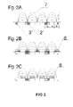
- the parameters of the impedimetric sensor depend on the geometry of the digitated electrodes; i.e., on the width of each digit and on the separation between digits (parameters a and b from Figure 2A ).
- the larger part of the signal is due to a region on the electrodes whose penetration in the medium is equal to the distance between the centres of two adjacent digitated electrodes, as described in Figured 2A, where the vector lines (7) are shown schematically.
- the typical length of the biomolecules is in the range of between 10 - 100 nm, which implies that for the case in which the molecules are immobilised in the space between each pair of digitated electrodes, the size of the digits and the separation between them have to be very small, which is difficult to achieve with conventional microelectronic technology.
- Another way to improve the sensitivity of the impedimetric sensitivity consists of using metallic or polymeric particles bonded to the molecule which is to be detected ( Wang JB, Profitt JA, Pugia MJ, et al. Au nanoparticle conjugation for impedance and capacitance signal amplification in biosensors ANALYTICAL CHEMISTRY 78 (6): 1769-1773 MAR 15 2006 ), as disclosed in patents US2002150886 , W02005001479 .
- the interaction between the marked molecules and the immobilised receptors on the sensor results in the production of a greater interference with the electrical field and, consequently, a greater sensitivity.
- a three-dimensional IDEA sensor is presented, formed from partially covered channels with a metal sheet and which, together with a metallic surface layer, make up the sensor electrodes. This geometry permits a redistribution of the analysed electrical field and an increase of the sensitivity of the sensor.
- biosensor of the invention for directly determining the presence of analytes in a sample, which comprises ( Figure 4 ):
- One specific object of the invention is constituted by the biosensor of the invention in which the insulating substrate from i) is of a material belonging, illustratively and without this limiting the scope of the invention, to the following group: a polymer, a glass or an inorganic oxide.
- Another specific object of the invention is constituted by the biosensor of the invention in which the substrate from i) is not of an insulating material but rather comprises an insulating or dielectric layer of a material belonging, illustratively and without this limiting the scope of the invention, to the following group: silicon dioxide or a polymer.
- Another specific object of the invention is constituted by the biosensor of the invention in which the highly conductive and inert electrodes from ii) are of a material belonging, illustratively and without this limiting the scope of the invention, to the following group: metals, preferably Pt, Pd and Au, oxides, Si, silicon polycrystalline, tantalum silicide or, even, polymer conductors.
- Another specific object of the present invention is constituted by the biosensor of the invention in which the electrodes have digits with a width and a separation between them between the ranges of 0.5 to 10.0 ⁇ m.
- Another specific object of the present invention is constituted by the biosensor of the invention in which the insulating barrier from iii) is of a material belonging, illustratively and without this limiting the scope of the invention, to the following group: inorganic oxides, polymers and materials sensitive to the exposure of UV light.
- Another specific object of the present invention is constituted by the biosensor of the invention in which the insulating barrier from iii) features a thickness of the insulating layer, which defines the height of the barrier which separates two adjacent digits, which means that it is between 50% and 150% of the distance which separates the centres of a pair of consecutive digitated electrodes, or more preferably, close to 100%.
- Another specific object of the present invention is constituted by the biosensor of the invention which further comprises a device or apparatus which detects the electrical properties connected to the electrodes from ii) whereto is applied an AC voltage, and which detects the variation in the electrical field close to the surface of the barriers, and a device or apparatus to apply said voltage.
- Another specific object of the present invention is constituted by the use of the biosensor of the invention, hereinafter use of the biosensor of analytes or molecules which are found in a biological sample.
- One objective of the present invention is that of providing a new electrochemical biosensor and a method capable of determining the presence or absence of molecular structures or analytes in a problem sample.
- the present invention is based on the fact that the inventors have observed that they can build a new highly sensitive electrochemical sensor whose operational principle is based on the interference which is produced between an electrical field generated between two electrodes and the molecular structures which can be formed due to the interaction of analytes from a sample in solution with the receptor molecules or immobilised sensors on the surface of the sensor, and in which the highly conductive electrodes are separated by a barrier of an insulating material (see Examples 1 to 3).
- the biochemical reactions which take place in said molecular interaction affect the distribution of ionic charges and, therefore, the electrical properties of the layers close to the surface of the barrier.
- An AC voltage is applied to the electrodes through a detection device whereto they are connected, detecting the impedance changes which are produced between them. Due to the presence of the insulating barrier, most of the current which flows between the electrodes passes through a thin layer very close to the surface of the barrier, which permits the increase of the sensitivity to the impedance changes derived from the biochemical processes.
- an object of the present invention is constituted by a useful biosensor to directly determine the presence of analytes in a sample, hereinafter biosensor of the invention, which comprises ( Figure 4 ):
- Receptor molecules in this invention are understood to be those operationally defined molecules which are capable of reacting or bonding to other molecules or analytes of a sample to form a complex and/or induce a secondary reaction.
- the receptor molecules can be enzymes, antibodies, antigens, peptides, DNA fragments, RNA fragments or oligonucleotides.
- the analytes or molecules to be determined in a solution or a sample can be any molecule present in the sample which bonds to or reacts with the receptor molecules.
- the analytes to be determined can be, illustratively and without limiting the scope of the invention, enzymes, antibodies, antigens, peptides, DNA fragments, RNA fragments, oligonucleotides or even complete cells of different types such as eukaryotes or prokaryotes.
- the bond between a receptor molecule and an analyte takes place, for example, in hybridisations of single DNA and/or RNA chains, antigen/antibody and enzyme/substrate reactions, within problem analyte identification procedures within a sample, preferably biological, of clinical or veterinarian, alimentary or environmental origin, amongst others.
- the substrate from i), called base layer can be of different types of materials, for example a crystalline wafer (quartz, silicon, sapphire), an amorphous material (glass), a polymer (PMMA, PCC, PEEK, PVE, PEI) or a thick layer of ceramic material, such as Al 2 O 3 .
- a crystalline wafer quartz, silicon, sapphire
- an amorphous material glass
- a polymer PMMA, PCC, PEEK, PVE, PEI
- a thick layer of ceramic material such as Al 2 O 3 .
- an insulating dielectric layer must be formed on the surface thereof.
- This insulating layer can be a polymeric layer, such as a polyimide or a BCB, or an inorganic material, for example Si 3 N 4 deposited by LPCVD or PECVD techniques, or a layer of SiO 2 deposited or grown thermally on a silicon wafer.
- One specific object of the invention is constituted by the biosensor of the invention in which the insulating substrate from i) is of a material belonging, illustratively and without this limiting the scope of the invention, to the following group: a polymer, a glass or an inorganic oxide.
- Another specific object of the invention is constituted by the biosensor of the invention in which the substrate from i) is not of an insulating material but rather comprises an insulating or dielectric layer of a material belonging, illustratively and without this limiting the scope of the invention, to the following group: silicon dioxide or a polymer.
- the electrodes from ii) are formed by a layer of a good electrical conducting material, deposited on the dielectric layer, preferably using evaporation techniques.
- the geometry of the electrodes is defined by means of lithographic techniques, followed by direct etching techniques or by lift-off.
- the width and separation between each pair of digitated electrodes must be of sizes which are preferably in the micrometric range; nevertheless, they can also be in the sub-micrometric range. Any material which is a good electrical conductor and which does not react with the solution can be used to form the electrodes.
- the thickness of the conductive layer can be very wide, but for the application as biochemical sensor a thickness of around 150 nm is recommended.
- the deposition of the layer can be achieved by means of thermal evaporation, cathode sputtering, electron gun or any other known technique which permits the production of layers of electrically conductive materials, and is within the scope of a person skilled in the art.
- Another specific object of the invention is constituted by the biosensor of the invention in which the highly conductive and inert electrodes from ii) are of a material belonging, illustratively and without this limiting the scope of the invention, to the following group: metals, preferably Pt, Pd and Au, oxides, Si, silicon polycrystalline, tantalum silicide or, even, polymer conductors.
- Another specific object of the present invention is constituted by the biosensor of the invention in which the electrodes have digits with a width and a separation between them between the ranges of 0.5 to 10.0 ⁇ m.
- a metallic layer is deposited on the surface of the sensor whose structural pattern is defined, using contrast masks and photolithographic processes and conventional etching.
- the metal of the welding point can be of any metal which guarantees a good threaded weld and a low contact resistance with the underlying material, which makes up the conductive electrodes.
- This metal as an example, can be aluminium.
- the dielectric barriers between each pair of adjacent electrodes of the interdigitated structure are created by means of depositing a layer of insulating material (15) which is eliminated on top of the metallic electrodes (digits) and of the welding points by means of using the photolithographic UV processes and etching, mainly deep reactive ion etching (DRIE).
- the thickness of the insulating layer which defines the height of the barrier which separates two adjacent digits, is supposedly equal to 100% of the distance which separates the centres of said pair of adjacent digitated electrodes.
- barriers with heights which vary from between 50% and 150% of the intercentral distance of two consecutive digits, or with thicknesses above or below this range.
- the dielectric material used to form the barriers can be any type of insulating material, although due to technological reasons it is preferable to use as such the silicon dioxide obtained via LPCVD, since it can be easily eliminated.
- the shape of the barriers produced after the etching process is also not critical, as these can be rectangular, with sloped or vertical walls, and flat or round in the upper part.
- Another specific object of the present invention is constituted by the biosensor of the invention in which the insulating barrier from iii) is of a material belonging, illustratively and without this limiting the scope of the invention, to the following group: inorganic oxides, polymers and materials sensitive to the exposure of UV light.
- Another specific object of the present invention is constituted by the biosensor of the invention in which the insulating barrier from iii) features a thickness of the insulating layer, which defines the height of the barrier which separates two adjacent digits, which means that it is between 50% and 150% of the distance which separates the centres of a pair of consecutive digitated electrodes, or more preferably, close to 100%.
- the receptor molecules from iv) (12, Figure 4 ) can be immobilised on the surface of the insulating barrier in accordance with the molecule immobilisation methods known in the state of the art, in the way of illustration and without limiting the scope of the invention: bonding by epoxide, carbodiimide, reduction refining, cyanogen bromide, succinimide, carbodiimidazol, tresyl and tosyl chloride, divinyl chloride, maleimide, hydrazide, iso(thio)cyanate and, preferably, by silinasation with amino silanes, epoxide silanes, thiocyanate and isothiocyanate silanes, succinic anhydride silanes, sulfhydryl silanes and caprolactam silanes.
- the receptor molecules consist of biological molecules which are capable of bonding to their corresponding analyte present in the biological sample to be analysed.
- Another alternative form of the sensor of the invention is that wherein the receptor molecules from iv) are immobilised on the surface of the electrodes.
- the described technological process permits, by means of the use of conventional microelectronic technology, a great miniaturization of the sensors and, also, the construction of arrays of these built-in sensors on a single substrate.
- the built-in sensor arrays manufactured following the described methodology permit the production of devices for microdiagnostics. These built-in devices are capable of simultaneously detecting a multitude of parameters, this is multi-parametric analysis. That has particular importance in situations where the sample is small and when one wants to carry out screening assays.
- Another specific object of the present invention is constituted by the biosensor of the invention wherein the electrodes are organized according to an interdigitated array.
- the variation of the electrical field of the biosensor upon producing the bond between the receptor molecule and the analyte can be quantified by measuring the impedance at a suitable frequency and/or DC polarization.
- the impedance analysis is the preferred electrical measurement, as this analysis can bring reveal the measurement of the resistance, capacity, dielectric and/or reactance loss, on a range of frequencies, including or not the DC polarization, or a combination of both techniques.
- Another specific object of the present invention is constituted by the biosensor of the invention which further comprises a device or apparatus which detects the electrical properties connected to the electrodes from iii) whereto is applied an AC voltage, and which detects the variation in the electrical field close to the surface of the barriers, and a device or apparatus to apply said voltage.
- Another specific embodiment is constituted by the biosensor of the invention wherein the detection device is an impedimeter which measures the impedance between the electrodes of the sensor.
- biosensor of the invention which comprises several biomolecular sensors, whether, because they are of different type of biomolecules, for example, a nucleic acid (for example, a probe or an oligonucleotide), antigens, antibodies, enzymes, proteins or peptides, or because being of the same type of molecule they head towards one or more different target molecules.
- a nucleic acid for example, a probe or an oligonucleotide
- antigens for example, antibodies, enzymes, proteins or peptides, or because being of the same type of molecule they head towards one or more different target molecules.
- Another specific object of the present invention is constituted by the use of the biosensor of the invention, hereinafter use of the biosensor of analytes or molecules which are found in a biological sample.
- the analytes to be determined can be, illustratively and without limiting the scope of the invention, enzymes, antibodies, antigens, peptides, DNA fragments, RNA fragments, oligonucleotides or, even, complete cells of different types such as eukaryotes or prokaryotes and their identification may be of interest for example in the field of diagnostics of human or veterinary illnesses, environmental analyses, forensic analyses, etc.
- Example 1 Manufacture of the impedimetric sensor of the invention.
- the starting material for this specific embodiment of the invention was a silicon wafer. Given that it is only going to be used as a substrate, neither the type nor the dose of the drug is important, nor is the conductivity value or the crystalline orientation.
- the silicon wafer was thermally oxidized, at 950oC in a wet oxidation process, forming a layer of 2500 nm of silicon dioxide of good dielectric quality.
- the next step consisted of depositing a layer of tantalum silicide, highly conductive, of 230 nm in thickness by means of cathode sputtering by magnetron.
- the first photolithographic level defined the collector bars and the digits of the two electrodes.
- the definition of the motives was made with the reactive ion etching techniques. As a result, an array with 216 digits was produced, each one 3.0 ⁇ m thick and others with 3.0 ⁇ m of distance between adjacent digits.
- the aperture between the electrodes was of 1.4 mm, and their total length was 301.0 mm for each electrode.
- the welding points were formed by depositing a layer of 1.0 ⁇ m of aluminium, and were disposed, by means of using conventional photolithographic and etching techniques, at the ends of the collector bars.
- the final step was producing the insulating barriers.
- the surface of the wafer was covered with a layer of, in this case, 4.0 ⁇ m of silicon oxide deposited by LPCVD.
- Photolithography and etching was once again used to create the pattern which permitted leaving the material between the digits and cover the collector bars, except at the welding points.
- the elimination of this layer was performed with the deep reactive ion etching (DRIE) technique, which provides barriers with almost vertical walls.
- DRIE deep reactive ion etching
- the individual devices were stuck to a PCB substrate and the threads were welded for the electrical connection with an impedimeter.
- Example 2 Use of the sensor of the invention as immunosensor.
- the electrodes were cleaned in a solution of 70% absolute ethanol and 30% Milli-Q water. Afterwards, the devices were submerged in a solution of 2.5% NaOH and Milli-Q water for 10 minutes, followed by a rinsing in 100 mL of Milli-Q water, in order to neutralize the action of the NaOH. Finally, the electrodes were cleaned in ethanol and dried in nitrogen current.
- the electrodes were introduced into a GPTS [(3-glycidoxipropil) trimethoxisilane] solution with 2.5% ethanol anhydride for three hours, at ambient temperature and with orbital agitation. After this time had passed, the devices were washed in ethanol and dried in nitrogen current.
- Biological molecular receptors were designed and produced to analyse antibiotics from the family of sulfamides.
- the preparation of the biological receptors was approached by means of the design of immunization haptens using molecular modelling strategies.
- the synthesis of 2 haptens or antigens was proposed.
- One of them (hapten 1) kept the greater part of the structure of the sulfamides, while the second (hapten 2) was only a fragment which conserved the part common to most of the compounds of this family of antibiotics.
- the two haptens were combined to the HCH (horseshoe crab hemocyanin) protein and to the BSA (bovine serum albumin) protein by using methods described in the literature.
- the covalent bonding of the haptens or antigens and the quantification of the number of the remainder of antigens bonded to the protein was carried out by means of a mass spectrometer. Following this, rabbits of the New Zealand variety were immunised with these antigens by applying a six-month long immunisation protocol, during which the progress of the immune response was controlled by means of extracting small blood samples.
- Sulfapyridine pattern solutions prepared in PBST (0.64 nM - 50000 nM, in PBST) were added to the electrodes (150 ⁇ L/electrode), followed by a solution with the specific sulfamide antiserum (#155) obtained (1/2000 in PBST, 150 ⁇ L/electrode). After incubating for 30 minutes, at ambient temperature, the devices were washed with PBST (three times, 1000 ⁇ L/electrode), and once with Mill-Q water (1000 ⁇ L/electrode). The reaction was measured in a low conductivity solution.
- the data which is shown in Table 1 represents the parameters characteristic of the immunoenzymatic assay ELISA and of the impedimetric immunosensor.
- the IC50 indicated the sensitivity, when the most sensitive value of the assay is the smallest.
- Another important parameter was the relationship between the maximum signal and the minimum signal, when the value is higher, the better the response of the device of the invention. Going back to comparing the immunosensor of the invention with the ELISA assay confirmed that there had been a better response from the immunosensor with respect to the ELISA.
- the R2 is presented, which indicates the degree of adjustment of the experimental data to the previously mentioned sigmoid curve, which ended up being identical.
- the electrodes were cleaned in a solution of 70% absolute ethanol and 30% Milli-Q water. Afterwards, the devices were submerged in a solution of 2.5% NaOH and Milli-Q water for 10 minutes, followed by a rinsing in 100 mL of Milli-Q water, in order to neutralize the action of the NaOH. Finally, the electrodes were cleaned in ethanol and dried in nitrogen current.
- the electrodes were introduced into a GPTS [(3-glycidoxipropil) trimethoxisilane] solution with 2.5% ethanol anhydride for three hours, at ambient temperature and with orbital agitation. After this time had passed, the devices were washed in ethanol and dried in nitrogen current.
- a single oligonucleotide chain of 20 pairs of bases was immobilised to the surface of the electrodes, with amine groups in position 5'.
- the oligos were 20 below: 5'-aminohexyl-CGA GTC ATT GAG TCA TCG AG-3'; and 20 above: 5'-fluoresceinahexyl.CTC GAT GAC TCA ATG ACT CG-3'.
- the hybridisation of the oligonucleotide was performed, in a buffer solution, with the complementary 20-base pair oligonucleotide, marked with fluorescein in position 5'.
- the electrodes were introduced in a solution containing the complementary oligonucleotide (10 ⁇ g/ml, 300 ⁇ L) and incubated for five minutes at ambient temperature. After this time, the devices were washed with a PBST buffer (1000 ⁇ L/electrode) and dried in dry nitrogen current. The determination of the hybridisation process was measured in a low conductivity solution. Table 2. Parameters of the oligonucleotides.
- Oligo 20 initial 20 complementary Length 20 20 GC (content, %) 50 50 Tm (50 mNa, oC) 52.6 52.6 Molecular Weight 6157 6157 Ext. Coefficient 198800 188400 mmol/OD 260 5.03 5.31 ⁇ g/ml 30.97 32.26 Table 3. Values obtained for the equivalent circuit elements of Figure 3, adjusted by means of the commercial programme: Zplot/Zview (Scribner Associates Inc.). Device Rs Rct Free 118000 3541 Funcionalized 29645 2645 With Oligonucleotide 50538 1889 Hybridised 43528 10014
Landscapes
- Health & Medical Sciences (AREA)
- Life Sciences & Earth Sciences (AREA)
- Chemical & Material Sciences (AREA)
- Immunology (AREA)
- Engineering & Computer Science (AREA)
- Molecular Biology (AREA)
- Physics & Mathematics (AREA)
- General Physics & Mathematics (AREA)
- Analytical Chemistry (AREA)
- Biochemistry (AREA)
- General Health & Medical Sciences (AREA)
- Biomedical Technology (AREA)
- Urology & Nephrology (AREA)
- Hematology (AREA)
- Pathology (AREA)
- Chemical Kinetics & Catalysis (AREA)
- Biotechnology (AREA)
- Microbiology (AREA)
- Medicinal Chemistry (AREA)
- Food Science & Technology (AREA)
- Cell Biology (AREA)
- Organic Chemistry (AREA)
- Electrochemistry (AREA)
- Zoology (AREA)
- Wood Science & Technology (AREA)
- Proteomics, Peptides & Aminoacids (AREA)
- Spectroscopy & Molecular Physics (AREA)
- Genetics & Genomics (AREA)
- General Engineering & Computer Science (AREA)
- Bioinformatics & Cheminformatics (AREA)
- Biophysics (AREA)
- Investigating Or Analyzing Materials By The Use Of Electric Means (AREA)
- Investigating Or Analysing Biological Materials (AREA)
Applications Claiming Priority (2)
| Application Number | Priority Date | Filing Date | Title |
|---|---|---|---|
| ES200701253A ES2307430B1 (es) | 2007-05-09 | 2007-05-09 | Biosensor y sus aplicaciones. |
| PCT/ES2008/070084 WO2008139016A1 (es) | 2007-05-09 | 2008-04-29 | Biosensor impedimétrico y sus aplicaciones |
Publications (2)
| Publication Number | Publication Date |
|---|---|
| EP2148191A1 true EP2148191A1 (de) | 2010-01-27 |
| EP2148191A4 EP2148191A4 (de) | 2013-11-27 |
Family
ID=39926854
Family Applications (1)
| Application Number | Title | Priority Date | Filing Date |
|---|---|---|---|
| EP08761596.9A Withdrawn EP2148191A4 (de) | 2007-05-09 | 2008-04-29 | Impedanzmesser und anwendungen dafür |
Country Status (5)
| Country | Link |
|---|---|
| US (1) | US8608919B2 (de) |
| EP (1) | EP2148191A4 (de) |
| JP (1) | JP5568466B2 (de) |
| ES (1) | ES2307430B1 (de) |
| WO (1) | WO2008139016A1 (de) |
Cited By (2)
| Publication number | Priority date | Publication date | Assignee | Title |
|---|---|---|---|---|
| WO2012151527A3 (en) * | 2011-05-05 | 2013-03-21 | Daktari Diagnostics, Inc. | Conductive patterns and methods for making conductive patterns |
| ES2498790A1 (es) * | 2013-03-20 | 2014-09-25 | Dropsens, S.L. | Procedimiento para la detección magneto-electroquímica sin lavados de un analito en una muestra |
Families Citing this family (17)
| Publication number | Priority date | Publication date | Assignee | Title |
|---|---|---|---|---|
| AUPS267802A0 (en) * | 2002-05-30 | 2002-06-20 | Bio-Molecular Holdings Pty Limited | Improved dna amplification apparatus and method |
| ES2367615B1 (es) | 2009-12-15 | 2013-01-22 | Consejo Superior De Investigaciones Científicas (Csic) | Sistema y procedimiento multianalítico basado en mediciones impedimétricas. |
| US9103773B2 (en) * | 2010-05-06 | 2015-08-11 | Seoul National University R&D Foundation | Capacitive element sensor and method for manufacturing same |
| ES2404944B1 (es) * | 2011-07-22 | 2014-08-11 | Consejo Superior De Investigaciones Científicas (Csic) | Sensor de determinación directa de la presencia de detergentes en una muestra |
| WO2013030930A1 (ja) * | 2011-08-29 | 2013-03-07 | トヨタ自動車株式会社 | 微粒子センサ及び微粒子センサの製造方法 |
| US9151759B2 (en) | 2013-05-06 | 2015-10-06 | Research Foundation Of The City University Of New York | Method for detecting cells with elastic cell membranes |
| US9746441B2 (en) * | 2013-05-13 | 2017-08-29 | Sony Corporation | Sensor, sensor kit and method for detecting an analyte |
| US10004433B2 (en) * | 2014-07-07 | 2018-06-26 | Verily Life Sciences Llc | Electrochemical sensor chip |
| US10196678B2 (en) | 2014-10-06 | 2019-02-05 | ALVEO Technologies Inc. | System and method for detection of nucleic acids |
| KR101755469B1 (ko) * | 2015-12-08 | 2017-07-07 | 현대자동차 주식회사 | 미세 물질 측정 센서 |
| KR101754239B1 (ko) * | 2015-12-28 | 2017-07-06 | 한국과학기술연구원 | 수용체와 표적 생체물질의 반응을 이용한 교차 전극 바이오센서 |
| CN109996888A (zh) | 2016-09-23 | 2019-07-09 | 阿尔韦奥科技公司 | 用于检测分析物的方法和组合物 |
| CA3041353A1 (en) | 2018-04-27 | 2019-10-27 | Innotech Alberta Inc. | Method and device for detecting a component in a sample |
| EP3899022A4 (de) | 2018-12-20 | 2023-03-01 | Alveo Technologies Inc. | Tragbares impedanzbasiertes diagnostisches testsystem zum nachweis von analyten |
| CN113008951B (zh) * | 2019-12-20 | 2024-04-19 | 利多(香港)有限公司 | 一种生物传感器及其在检测血液样品凝血指标中的应用 |
| US12472492B2 (en) | 2020-08-14 | 2025-11-18 | Alveo Technologies, Inc. | Systems and methods of sample depositing and testing |
| BR102021002128A2 (pt) * | 2021-02-04 | 2022-08-16 | Cnpem - Centro Nacional De Pesquisa Em Energia E Materiais | Biossensor sem marcação baseado em estrutura de imidazolato zeolítico, processo de fabricação do mesmo e processo de detecção de interações proteína-proteína |
Family Cites Families (24)
| Publication number | Priority date | Publication date | Assignee | Title |
|---|---|---|---|---|
| US4571543A (en) | 1983-03-28 | 1986-02-18 | Southwest Medical Products, Inc. | Specific material detection and measuring device |
| US4794089A (en) | 1986-03-25 | 1988-12-27 | Midwest Research Microscopy, Inc. | Method for electronic detection of a binding reaction |
| JPH02223855A (ja) * | 1989-02-23 | 1990-09-06 | Nec Corp | イオンセンサ |
| US5846708A (en) * | 1991-11-19 | 1998-12-08 | Massachusetts Institiute Of Technology | Optical and electrical methods and apparatus for molecule detection |
| IL103674A0 (en) | 1991-11-19 | 1993-04-04 | Houston Advanced Res Center | Method and apparatus for molecule detection |
| WO1997021094A1 (en) * | 1995-12-01 | 1997-06-12 | Innogenetics N.V. | Impedimetric detection system and method of production thereof |
| EP1019715B1 (de) * | 1997-08-08 | 2005-01-26 | California Institute Of Technology | Techniken und systeme zum nachweis von analyten |
| CN1419651A (zh) * | 2000-03-22 | 2003-05-21 | 全麦迪科斯有限责任公司 | 带有识别电极的电化生物传感器试验片以及采用该试验片的示读仪 |
| US6835552B2 (en) | 2000-12-14 | 2004-12-28 | The Regents Of The University Of California | Impedance measurements for detecting pathogens attached to antibodies |
| US20040023253A1 (en) * | 2001-06-11 | 2004-02-05 | Sandeep Kunwar | Device structure for closely spaced electrodes |
| US6946067B2 (en) * | 2002-01-04 | 2005-09-20 | Lifescan, Inc. | Method of forming an electrical connection between an electrochemical cell and a meter |
| US20040110277A1 (en) | 2002-04-12 | 2004-06-10 | Seiko Epson Corporation | Sensor cell, bio-sensor, capacitance element manufacturing method, biological reaction detection method and genetic analytical method |
| DE50305588D1 (de) * | 2002-06-24 | 2006-12-14 | Siemens Ag | Biosensor-array und verfahren zum betreiben eines biosensor-arrays |
| WO2004025262A2 (en) * | 2002-09-11 | 2004-03-25 | Synamem Corporation | Membrane-based assays |
| WO2004044570A1 (ja) | 2002-11-14 | 2004-05-27 | Toyama Prefecture | ハイブリダイゼーションの検出方法 |
| AT413214B (de) | 2003-01-24 | 2005-12-15 | Sy Lab Vgmbh | Messanordnung und verfahren zur detektion einer dna-sequenz |
| DE10328136A1 (de) | 2003-06-23 | 2005-01-27 | Infineon Technologies Ag | Sensor-Element, Sensor-Array und Verfahren zum Erfassen von in einem Analyten möglicherweise enthaltenen Partikeln |
| US8288544B2 (en) | 2003-07-01 | 2012-10-16 | Roche Diagnostics Operations, Inc. | Electrochemical affinity biosensor system and methods |
| US7390622B2 (en) * | 2003-10-16 | 2008-06-24 | Hai Kang Life Corporation Limited | Apparatus and methods for detecting nucleic acid in biological samples |
| US7981362B2 (en) * | 2003-11-04 | 2011-07-19 | Meso Scale Technologies, Llc | Modular assay plates, reader systems and methods for test measurements |
| DE102004005711A1 (de) | 2004-02-05 | 2006-05-11 | Siemens Ag | Biosensor zur Bestimmung eines Allergenes mit Betriebsverfahren |
| EP2278310B1 (de) * | 2004-06-18 | 2016-11-16 | Sensirion Holding AG | Kapazitiver Sensor |
| JP4585280B2 (ja) * | 2004-11-08 | 2010-11-24 | 一般社団法人オンチップ・セロミクス・コンソーシアム | 細胞チップおよび細胞改変方法および細胞制御方法 |
| EP1772732A1 (de) * | 2005-10-07 | 2007-04-11 | Innogenetics N.V. | Polymer-replizierte verflochtene Elektroden-Arrays für (Bio)-Sensoranwendungen |
-
2007
- 2007-05-09 ES ES200701253A patent/ES2307430B1/es not_active Expired - Fee Related
-
2008
- 2008-04-29 WO PCT/ES2008/070084 patent/WO2008139016A1/es not_active Ceased
- 2008-04-29 JP JP2010506958A patent/JP5568466B2/ja not_active Expired - Fee Related
- 2008-04-29 EP EP08761596.9A patent/EP2148191A4/de not_active Withdrawn
- 2008-04-29 US US12/599,378 patent/US8608919B2/en not_active Expired - Fee Related
Cited By (3)
| Publication number | Priority date | Publication date | Assignee | Title |
|---|---|---|---|---|
| WO2012151527A3 (en) * | 2011-05-05 | 2013-03-21 | Daktari Diagnostics, Inc. | Conductive patterns and methods for making conductive patterns |
| US9221050B2 (en) | 2011-05-05 | 2015-12-29 | Daktari Diagnostics, Inc. | Conductive patterns and methods for making conductive patterns |
| ES2498790A1 (es) * | 2013-03-20 | 2014-09-25 | Dropsens, S.L. | Procedimiento para la detección magneto-electroquímica sin lavados de un analito en una muestra |
Also Published As
| Publication number | Publication date |
|---|---|
| JP2010526311A (ja) | 2010-07-29 |
| US8608919B2 (en) | 2013-12-17 |
| JP5568466B2 (ja) | 2014-08-06 |
| ES2307430A1 (es) | 2008-11-16 |
| ES2307430B1 (es) | 2009-10-20 |
| EP2148191A4 (de) | 2013-11-27 |
| WO2008139016A1 (es) | 2008-11-20 |
| US20100193378A1 (en) | 2010-08-05 |
Similar Documents
| Publication | Publication Date | Title |
|---|---|---|
| US8608919B2 (en) | Impedimetric sensor and applications thereof | |
| US7575720B2 (en) | Capacitance based biosensor | |
| Pänke et al. | Impedance spectroscopy and biosensing | |
| Ingebrandt et al. | Label‐free detection of DNA using field‐effect transistors | |
| JP4768226B2 (ja) | 検体の高感度検出のために特別に構成されたゲート電極を有するfetセンサー | |
| US7732140B2 (en) | Method for direct electrical detection of molecules and molecule-molecule interactions | |
| US20020028441A1 (en) | Detection of molecules and molecule complexes | |
| US20090191616A1 (en) | Biosensor structure and fabricating method thereof | |
| US20050136419A1 (en) | Method and apparatus for nanogap device and array | |
| US20100260745A1 (en) | Methods of using and constructing nanosensor platforms | |
| Li et al. | Impedance labelless detection-based polypyrrole protein biosensor | |
| Kachhawa et al. | Antigen-antibody interaction-based GaN HEMT biosensor for C3G detection | |
| US11592415B2 (en) | Bio-sensor having interdigitated microelectrode using response of receptor and target bioproducts | |
| JP2001510564A (ja) | 生物学的分析用のマイクロシステム及びその製造方法 | |
| JP4482856B2 (ja) | 試料中の標的物質の検出方法、センサ基体、及び検出キット | |
| Bratov et al. | Impedimetric sensor and applications thereof | |
| Fang et al. | Dielectric film for biosensor application | |
| US20190120788A1 (en) | Systems and methods for fabricating an indium oxide field-effect transistor | |
| KR20110128754A (ko) | 극미량 시료 검출용 전기 바이오센서 | |
| Di Carlo et al. | Nanogap-based dielectric immunosensing | |
| Vermeeren et al. | Evolution towards the implementation of point-of-care biosensors | |
| KR100964202B1 (ko) | 티타늄 박막을 이용한 fet형 바이오센서 및 그 제조방법 | |
| Vinzons et al. | Semiconductor Biosensors Based on Nanowire Field-Effect Transistors | |
| Macchia et al. | Effect of the ionic-strength of the gating-solution on a bioelectronic response | |
| Prince | Characterization of electrodeposited polyaniline biosensor platform for Escherichia coli O157: H7 detection |
Legal Events
| Date | Code | Title | Description |
|---|---|---|---|
| PUAI | Public reference made under article 153(3) epc to a published international application that has entered the european phase |
Free format text: ORIGINAL CODE: 0009012 |
|
| 17P | Request for examination filed |
Effective date: 20091119 |
|
| AK | Designated contracting states |
Kind code of ref document: A1 Designated state(s): AT BE BG CH CY CZ DE DK EE ES FI FR GB GR HR HU IE IS IT LI LT LU LV MC MT NL NO PL PT RO SE SI SK TR |
|
| AX | Request for extension of the european patent |
Extension state: AL BA MK RS |
|
| DAX | Request for extension of the european patent (deleted) | ||
| A4 | Supplementary search report drawn up and despatched |
Effective date: 20131030 |
|
| RIC1 | Information provided on ipc code assigned before grant |
Ipc: G01N 33/543 20060101ALI20131024BHEP Ipc: C12Q 1/00 20060101ALI20131024BHEP Ipc: G01R 27/16 20060101ALI20131024BHEP Ipc: G01N 27/327 20060101ALI20131024BHEP Ipc: G01N 27/02 20060101AFI20131024BHEP |
|
| 17Q | First examination report despatched |
Effective date: 20160705 |
|
| STAA | Information on the status of an ep patent application or granted ep patent |
Free format text: STATUS: EXAMINATION IS IN PROGRESS |
|
| STAA | Information on the status of an ep patent application or granted ep patent |
Free format text: STATUS: THE APPLICATION IS DEEMED TO BE WITHDRAWN |
|
| 18D | Application deemed to be withdrawn |
Effective date: 20161116 |