EP2154503B1 - Kapazitiver Verformungssensor - Google Patents
Kapazitiver Verformungssensor Download PDFInfo
- Publication number
- EP2154503B1 EP2154503B1 EP09010183.3A EP09010183A EP2154503B1 EP 2154503 B1 EP2154503 B1 EP 2154503B1 EP 09010183 A EP09010183 A EP 09010183A EP 2154503 B1 EP2154503 B1 EP 2154503B1
- Authority
- EP
- European Patent Office
- Prior art keywords
- electrodes
- dielectric layer
- electrode
- capacitive sensor
- back side
- Prior art date
- Legal status (The legal status is an assumption and is not a legal conclusion. Google has not performed a legal analysis and makes no representation as to the accuracy of the status listed.)
- Active
Links
Images








Classifications
-
- G—PHYSICS
- G01—MEASURING; TESTING
- G01L—MEASURING FORCE, STRESS, TORQUE, WORK, MECHANICAL POWER, MECHANICAL EFFICIENCY, OR FLUID PRESSURE
- G01L1/00—Measuring force or stress, in general
- G01L1/14—Measuring force or stress, in general by measuring variations in capacitance or inductance of electrical elements, e.g. by measuring variations of frequency of electrical oscillators
- G01L1/142—Measuring force or stress, in general by measuring variations in capacitance or inductance of electrical elements, e.g. by measuring variations of frequency of electrical oscillators using capacitors
-
- G—PHYSICS
- G01—MEASURING; TESTING
- G01B—MEASURING LENGTH, THICKNESS OR SIMILAR LINEAR DIMENSIONS; MEASURING ANGLES; MEASURING AREAS; MEASURING IRREGULARITIES OF SURFACES OR CONTOURS
- G01B7/00—Measuring arrangements characterised by the use of electric or magnetic techniques
- G01B7/16—Measuring arrangements characterised by the use of electric or magnetic techniques for measuring the deformation in a solid, e.g. by resistance strain gauge
- G01B7/22—Measuring arrangements characterised by the use of electric or magnetic techniques for measuring the deformation in a solid, e.g. by resistance strain gauge using change in capacitance
-
- G—PHYSICS
- G01—MEASURING; TESTING
- G01D—MEASURING NOT SPECIALLY ADAPTED FOR A SPECIFIC VARIABLE; ARRANGEMENTS FOR MEASURING TWO OR MORE VARIABLES NOT COVERED IN A SINGLE OTHER SUBCLASS; TARIFF METERING APPARATUS; MEASURING OR TESTING NOT OTHERWISE PROVIDED FOR
- G01D5/00—Mechanical means for transferring the output of a sensing member; Means for converting the output of a sensing member to another variable where the form or nature of the sensing member does not constrain the means for converting; Transducers not specially adapted for a specific variable
- G01D5/12—Mechanical means for transferring the output of a sensing member; Means for converting the output of a sensing member to another variable where the form or nature of the sensing member does not constrain the means for converting; Transducers not specially adapted for a specific variable using electric or magnetic means
- G01D5/14—Mechanical means for transferring the output of a sensing member; Means for converting the output of a sensing member to another variable where the form or nature of the sensing member does not constrain the means for converting; Transducers not specially adapted for a specific variable using electric or magnetic means influencing the magnitude of a current or voltage
- G01D5/24—Mechanical means for transferring the output of a sensing member; Means for converting the output of a sensing member to another variable where the form or nature of the sensing member does not constrain the means for converting; Transducers not specially adapted for a specific variable using electric or magnetic means influencing the magnitude of a current or voltage by varying capacitance
- G01D5/241—Mechanical means for transferring the output of a sensing member; Means for converting the output of a sensing member to another variable where the form or nature of the sensing member does not constrain the means for converting; Transducers not specially adapted for a specific variable using electric or magnetic means influencing the magnitude of a current or voltage by varying capacitance by relative movement of capacitor electrodes
- G01D5/2412—Mechanical means for transferring the output of a sensing member; Means for converting the output of a sensing member to another variable where the form or nature of the sensing member does not constrain the means for converting; Transducers not specially adapted for a specific variable using electric or magnetic means influencing the magnitude of a current or voltage by varying capacitance by relative movement of capacitor electrodes by varying overlap
-
- G—PHYSICS
- G01—MEASURING; TESTING
- G01L—MEASURING FORCE, STRESS, TORQUE, WORK, MECHANICAL POWER, MECHANICAL EFFICIENCY, OR FLUID PRESSURE
- G01L1/00—Measuring force or stress, in general
- G01L1/14—Measuring force or stress, in general by measuring variations in capacitance or inductance of electrical elements, e.g. by measuring variations of frequency of electrical oscillators
- G01L1/142—Measuring force or stress, in general by measuring variations in capacitance or inductance of electrical elements, e.g. by measuring variations of frequency of electrical oscillators using capacitors
- G01L1/146—Measuring force or stress, in general by measuring variations in capacitance or inductance of electrical elements, e.g. by measuring variations of frequency of electrical oscillators using capacitors for measuring force distributions, e.g. using force arrays
-
- G—PHYSICS
- G01—MEASURING; TESTING
- G01L—MEASURING FORCE, STRESS, TORQUE, WORK, MECHANICAL POWER, MECHANICAL EFFICIENCY, OR FLUID PRESSURE
- G01L5/00—Apparatus for, or methods of, measuring force, work, mechanical power, or torque, specially adapted for specific purposes
- G01L5/22—Apparatus for, or methods of, measuring force, work, mechanical power, or torque, specially adapted for specific purposes for measuring the force applied to control members, e.g. control members of vehicles, triggers
- G01L5/226—Apparatus for, or methods of, measuring force, work, mechanical power, or torque, specially adapted for specific purposes for measuring the force applied to control members, e.g. control members of vehicles, triggers to manipulators, e.g. the force due to gripping
- G01L5/228—Apparatus for, or methods of, measuring force, work, mechanical power, or torque, specially adapted for specific purposes for measuring the force applied to control members, e.g. control members of vehicles, triggers to manipulators, e.g. the force due to gripping using tactile array force sensors
-
- G—PHYSICS
- G06—COMPUTING OR CALCULATING; COUNTING
- G06F—ELECTRIC DIGITAL DATA PROCESSING
- G06F3/00—Input arrangements for transferring data to be processed into a form capable of being handled by the computer; Output arrangements for transferring data from processing unit to output unit, e.g. interface arrangements
- G06F3/01—Input arrangements or combined input and output arrangements for interaction between user and computer
- G06F3/03—Arrangements for converting the position or the displacement of a member into a coded form
- G06F3/041—Digitisers, e.g. for touch screens or touch pads, characterised by the transducing means
- G06F3/044—Digitisers, e.g. for touch screens or touch pads, characterised by the transducing means by capacitive means
- G06F3/0445—Digitisers, e.g. for touch screens or touch pads, characterised by the transducing means by capacitive means using two or more layers of sensing electrodes, e.g. using two layers of electrodes separated by a dielectric layer
-
- G—PHYSICS
- G06—COMPUTING OR CALCULATING; COUNTING
- G06F—ELECTRIC DIGITAL DATA PROCESSING
- G06F3/00—Input arrangements for transferring data to be processed into a form capable of being handled by the computer; Output arrangements for transferring data from processing unit to output unit, e.g. interface arrangements
- G06F3/01—Input arrangements or combined input and output arrangements for interaction between user and computer
- G06F3/03—Arrangements for converting the position or the displacement of a member into a coded form
- G06F3/041—Digitisers, e.g. for touch screens or touch pads, characterised by the transducing means
- G06F3/044—Digitisers, e.g. for touch screens or touch pads, characterised by the transducing means by capacitive means
- G06F3/0446—Digitisers, e.g. for touch screens or touch pads, characterised by the transducing means by capacitive means using a grid-like structure of electrodes in at least two directions, e.g. using row and column electrodes
-
- A—HUMAN NECESSITIES
- A61—MEDICAL OR VETERINARY SCIENCE; HYGIENE
- A61B—DIAGNOSIS; SURGERY; IDENTIFICATION
- A61B5/00—Measuring for diagnostic purposes; Identification of persons
- A61B5/103—Measuring devices for testing the shape, pattern, colour, size or movement of the body or parts thereof, for diagnostic purposes
- A61B5/11—Measuring movement of the entire body or parts thereof, e.g. head or hand tremor or mobility of a limb
-
- G—PHYSICS
- G06—COMPUTING OR CALCULATING; COUNTING
- G06F—ELECTRIC DIGITAL DATA PROCESSING
- G06F2203/00—Indexing scheme relating to G06F3/00 - G06F3/048
- G06F2203/041—Indexing scheme relating to G06F3/041 - G06F3/045
- G06F2203/04103—Manufacturing, i.e. details related to manufacturing processes specially suited for touch sensitive devices
Definitions
- the constitution described in (1) may preferably further include stretchable conductors connected respectively to the pair of electrodes, wherein each of the conductors contains an elastomer and conductive particles filled into the elastomer, has a smaller electric resistance than the electric resistance of the electrodes, and is formed by the printing method using a conductor coating containing a formation component of the conductor.
- the surface side conductor and the back side conductor are formed to include an elastomer and conductive particles filled into the elastomer, and therefore, when a load is applied from a measurement subject, the surface side conductor and the back side conductor can expand and contract in accordance with the load. Hence, the surface side conductor and the back side conductor are unlikely to restrict expansion and contraction of the dielectric layer.
- the elastomer serving as the material of the dielectric layer may preferably include one or more materials selected from silicone rubber, acrylonitrile-butadiene copolymer rubber, acrylic rubber, epichlorohydrin rubber, chlorosulfonated polyethylene, chlorinated polyethylene, and urethane rubber. According to this constitution, the specific dielectric constant of the dielectric layer is large, enabling an increase in the electrostatic capacity.
- the conductive fillers included in the surface side electrode and the back side electrode may be preferably non-metallic conductive fillers.
- the electric resistance of the surface side electrode and the back side electrode is larger than that of a case in which the surface side electrode and the back side electrode contain metallic conductive fillers. More specifically, the electric resistance corresponding to the distance from the surface side connection portion of the surface side electrode to the detection portion, and the electric resistance corresponding to the distance from the back side connection portion of the back side electrode to the detection portion increase. The electric resistance is separated from the detected impedance, and therefore, according to this constitution, the measurement precision of the surface pressure distribution is high even though the electric resistance of the surface side electrode and the back side electrode is large.
- the surface side electrode and the surface side conductor may be preferably printed onto a surface of the dielectric layer, and back side electrode and the back side conductor may be preferably printed onto a back of the dielectric layer.
- the surface side electrode and the back side electrode are printed directly onto the dielectric layer, and therefore positioning of the surface side electrode and the back side electrode can be performed easily. Hence, the detection portions can be arranged accurately in desired positions.
- the sensor main body may preferably further include a tubular insulating tube member that insulates an interior and an exterior of the insulating tube member, and the dielectric layer may be preferably housed in the insulating tube member.
- the surface side electrode and the surface side conductor may be preferably printed onto an inner surface of the insulating tube member in a portion facing the surface of the dielectric layer, and the back side electrode and the back side conductor are preferably printed onto the inner surface of the insulating tube member in a portion facing the back of the dielectric layer.
- At least one of the surface side electrode and the back side electrode may be preferably constituted by the elastomer composition containing the elastomer and the conductive fillers described above, and in the percolation curve expressing the relationship between the blended amount of the conductive fillers and the electric resistance in the elastomer composition, the blended amount (critical volume fraction: ⁇ c) of the conductive fillers at the first polarity change point at which the electric resistance decreases to cause the transition between insulator and conductor is 25vol% or less.
- a capacitive sensor according to the present invention may be used for various applications, including, a soft surface pressure sensor for artificial skin or the like, motion capture for detecting human movement, an information input device such as a keyboard, a seating sensor, a collision detection sensor for a vehicle, a surface pressure distribution sensor for a bed or a carpet, and so on.
- Preferred embodiments of the capacitive sensor according to the present invention will be hereinafter described. First, embodiments of the capacitive sensor according to the first aspect of the present invention (the first capacitive sensor) will be described, followed by embodiments of the capacitive sensor according to the second aspect of the present invention (the second capacitive sensor).
- An elastomer containing a polar functional group such as an ester group, a carboxyl group, a hydroxyl group, a halogen group, an amide group, a sulfone group, a urethane group, or a nitrile group, or an elastomer to which a polar low molecular weight compound containing these polar functional groups is added, for example, may be employed favorably.
- the elastomer may be crosslinked or not crosslinked. Further, by adjusting the Young's modulus of the elastomer, the detection sensitivity and the detection range can be adjusted in accordance with the application. For example, by employing a foam body having a small Young's modulus, small deformation can be detected easily.
- elastomer examples include silicone rubber, acrylonitrile-butadiene copolymer rubber, acrylic rubber, epichlorohydrin rubber, chlorosulfonated polyethylene, chlorinated polyethylene, and urethane rubber.
- the electrode elastomer preferably has a critical volume fraction ( ⁇ c) of 25vol% or less in a percolation curve when a mixture (elastomer composition) of the elastomer and conductive fillers is prepared.
- ⁇ c critical volume fraction
- Examples of the conductive fillers blended with the elastomer may include a carbon material and a metal.
- One of these materials may be used individually, or two or more of the materials may be mixed, as the conductive fillers.
- a carbon material is preferably used due to its comparatively low cost and the ease to form a conductive path.
- Carbon black exhibiting superior conductivity, such as ketjen black, for example, is preferable as the carbon material since such type of carbon black has a small particle diameter and aggregates easily.
- the elastomer constituting the conductor may be the same as the elastomer used for the dielectric layer and the electrode or may be different.
- Suitable examples of the elastomer include silicone rubber, ethylene-propylene copolymer rubber, natural rubber, styrene-butadiene copolymer rubber, acrylonitrile-butadiene copolymer rubber, acrylic rubber, epichlorohydrin rubber, chlorosulfonated polyethylene, chlorinated polyethylene, and urethane rubber.
- the first capacitive sensor according to the present invention may include an insulating layer for insulating the electrodes and the conductors from the outside.
- the insulating layer may be arranged to cover the electrode and the conductor arranged on at least one of the surface and the back of the dielectric layer.
- a film that possesses an insulating property and is elastically deformable is preferably employed as the insulating layer.
- the thickness of the formed dielectric layer, electrode, and so on may be increased by applying the coating in multiple layers.
- the printing method include screen printing, inkjet printing, flexographic printing, gravure printing, pad printing, and lithography. Of these methods, the screen printing method is preferable, because a highly viscous coating material can be used and it is easy to adjust the thickness of the coated film.
- the dielectric layer coating may be prepared by blending the formation components (elastomer, additives, and so on) of the dielectric layer with a solvent.
- the electrode coating and the conductor coating may be prepared by blending the respective formation components thereof with a solvent.
- a solid concentration of the respective coatings may be adjusted appropriately to achieve a viscosity suitable for the printing method employed.
- the dielectric layer, the electrode, and the conductor are respectively printed onto the surface of a substrate.
- the conductor coating is printed onto the surface of the substrate, dried, and crosslinked.
- the electrode coating is printed onto the surface, dried, and crosslinked.
- the dielectric layer coating is printed onto a surface of the formed electrode, dried, and crosslinked.
- the electrode coating is printed onto the surface of the formed dielectric layer, dried, and crosslinked.
- the conductor coating is then printed so as to connect to the uppermost electrode, dried, and crosslinked. If necessary, an insulating layer is then formed so as to cover the electrode and the conductor that are exposed.
- the elastic substrates are stacked onto both surfaces of the dielectric layer such that the formed electrodes contact the surface and the back of the dielectric layer (an elastomer sheet), respectively. More specifically, in a capacitive sensor manufactured using the third method, the pair of elastic substrates are arranged via the dielectric layer such that the electrode and the conductor that contact the surface of the dielectric layer are printed onto the back of one elastic substrate and the electrode and the conductor that contact the back of the dielectric layer are printed onto the surface of the other elastic substrate.
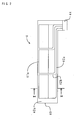
- FIG. 2 is a top view of the capacitive sensor.
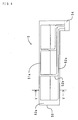
- FIG. 3 is a sectional view taken along the line III-III of Fig. 2 .
- a capacitive sensor 4 includes a dielectric layer 40, a pair of electrodes 41 a, 41b, conductors 42a, 42b, and cover films 43a, 43b.
- the dielectric layer 40 is made from urethane rubber and takes a belt shape extending in a left-right direction.
- the thickness of the dielectric layer 40 is approximately 300 ⁇ m.
- the electrode 41a takes a rectangular shape. Three electrodes 41a are formed on an upper surface of the dielectric layer 40 using screen printing. Similarly, the electrode 41b takes a rectangular shape. Three electrodes 41b are formed on a lower surface of the dielectric layer 40 so as to oppose the respective electrodes 41 a via the dielectric layer 40. The electrodes 41b are screen-printed onto the lower surface of the dielectric layer 40. Thus, three pairs of the electrodes 41a, 41b are arranged such that the electrodes 41 a, 41 b sandwich the dielectric layer 40.
- the cover film 43a is made of acrylic rubber and takes a belt shape extending in the left-right direction.
- the cover film 43a covers the upper surface of the dielectric layer 40, the electrodes 41a, and the conductor 42a.
- the cover film 43b is made of acrylic rubber and takes a belt shape extending in the left-right direction.
- the cover film 43b covers the lower surface of the dielectric layer 40, the electrodes 41b, and the conductor 42b.
- the cover films 43a, 43b are included in an insulating layer according to the present invention.
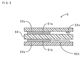
- a capacitive sensor according to this embodiment differs from the capacitive sensor according to the first embodiment by the constitution in which the electrodes and the conductors are formed on the elastic substrate, instead of the dielectric layer. Therefore, only this difference will be hereinafter described.
- the upper elastic substrate 53a and the lower elastic substrate 53b are made of acrylic rubber and take a belt shape extending in the left-right direction.
- Three electrodes 51a and three conductors 52a are formed on a lower surface of the upper elastic substrate 53a by screen printing. Each of the electrodes 51a is connected to an upper connector 54 by the corresponding conductor 52a.
- Three electrodes 51b and three conductors 52b are formed on an upper surface of the lower elastic substrate 53b by screen printing. Each of the electrodes 51b is connected to a lower connector (not shown) by the corresponding conductor 52b.
- the dielectric layer 50 is interposed between the upper elastic substrate 53a and the lower elastic substrate 53b.
- the dielectric layer 50 is made of foamed urethane rubber and takes a belt shape extending in the left-right direction.
- the thickness of the dielectric layer 50 is approximately 300 ⁇ m.
- An upper surface of the dielectric layer 50 contacts the electrodes 51a.
- a lower surface of the dielectric layer 50 contacts the electrodes 51 b.
- the capacitive sensor 5 according to this embodiment exhibits similar advantageous effects to those of the capacitive sensor according to the first embodiment in relation to portions having common constitutions. Furthermore, according to the capacitive sensor 5 of this embodiment, printing is not performed directly onto the dielectric layer 50. Therefore, a material that is not suitable for printing, such as a foam body, can be used as the dielectric layer 50. Hence, the freedom of material selection of the dielectric layer 50 is improved.
- FIG. 6 is a perspective top view of the capacitive sensor according to this embodiment. Note that in FIG. 6 , a surface side insulating cover layer and a back side insulating cover layer have been omitted. Further, a back side electrode and a back side conductor are indicated by thin lines, and detection portions are shown as the hatched portions.
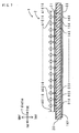
- FIG 7 is a sectional view taken along the line VII-VII of FIG. 6 . Note that in FIG. 7 , the thickness of a sensor main body in an up-down direction is emphasized. As shown in FIGS. 6 and 7 , a capacitive sensor 1 according to this embodiment includes a sensor main body 2 and a calculation portion 3.
- the sensor main body 2 includes a dielectric layer 20, surface side electrodes 01X to 16X, back side electrodes 01Y to 16Y, detection portions A0101 to A 1616, surface side conductors 01x to 16x, back side conductors 01y to 16y, a surface side insulating cover layer 21, a back side insulating cover layer 22, a connector for surface side conductor 23, and a connector for back side conductor 24.
- the first two digits "00” correspond to the surface side electrodes 01X to 16X
- the latter two digits "XX” correspond to the back side electrodes 0 1 Y to 16Y.
- a total of 16 back side conductors 01y to 16y are arranged on the lower surface of the dielectric layer 20.
- the back side conductors 01y to 16y are each formed to include urethane rubber and silver powder.
- the back side conductors 01y to 16y each take a linear shape.
- the connector for back side conductor 24 is arranged at a left front corner of the dielectric layer 20.
- the back side conductors 01y to 16y are respectively connected to the back side connection portions 01Y1 to 16Y and the connector for back side conductor 24.
- the back side insulating cover layer 22 is arranged on the back side of the dielectric layer 20.
- the back side insulating cover layer 22 is formed to include acrylic rubber.
- the back side insulating cover layer 22 takes a sheet form.
- the back side insulating cover layer 22 covers the dielectric layer 20, the back side electrodes 01Y to 16Y, and the back side conductors 01y to 16y from below.
- the detection portions A0101 to A1616 are arranged in portions (overlapping portions) in which the surface side electrodes 0 1 X to 16X and the back side electrodes 0 1 Y to 16Y intersect in the up-down direction.
- the detection portions A0101 to A1616 are arranged at substantially equal intervals over substantially the entire surface of the sensor main body 2.
- Each detection portion A0101 to A161616 partially includes the surface side electrode 01X to 16X, the back side electrode 0 1 Y to 16Y, and the dielectric layer 20.
- the power supply circuit 30 applies a sine wave-shaped alternating current voltage to the detection portions A0101 to A1616.
- a map indicating correspondence between electrostatic capacity and surface pressure in the detection portions A0101 to A1616 is stored in advance in the ROM 33.
- the ROM 33 also stores the following Equations (3) and (5). Impedance values and phase values input from the connector for surface side conductor 23 and the connector for back side conductor 24 are stored temporarily in the RAM 32.
- the CPU 31 extracts the electrostatic capacity of the detection portions A0101 to A1616 on the basis of the impedance and the phase values stored in the RAM 32 using Equations (3) and (5), as will be described below.
- the CPU 31 then calculates a surface pressure distribution of the sensor main body 2 from the electrostatic capacity.
- the display 34 displays the surface pressure distribution calculated by the CPU 31 on a screen (not shown), in the form of a three-dimensional graph, for example.
- the conductor coating is prepared using the following procedure. First, 333 parts by mass of a polymer (obtained by dissolving polyurethane in MEK/toluene/isopropyl alcohol; product name Nippolan (registered trademark) 5230, manufactured by Nippon Polyurethane Industry Co., Ltd.) (the solid content of the polymer is 30% by mass, and therefore 333 parts by mass of the polymer corresponds to 100 parts by mass of polyurethane), 400 parts by mass of 10 ⁇ m flaked silver powder (product name FA-D-4, manufactured by DOWA Electronics Materials Co., Ltd.), 400 parts by mass of spherical silver powder at 1 ⁇ m (product name AG2-1C, manufactured by DOWA Electronics Materials Co., Ltd.), and 150 parts by mass of a printing solvent (butyl carbitol, manufactured by Sankyo Chemical Co., Ltd.) are weighed and stirred until evenly mixed.
- a printing solvent butyl carbitol, manufactured by Sankyo Chemical Co., Ltd
- FIG. 8 is a pattern diagram showing the first half of the surface side electrode printing step in the manufacturing method for the capacitive sensor according to this embodiment.
- FIG. 9 is a pattern diagram showing the latter half of the step.
- the screen printer 9 is used to print the electrode coating 80 prepared in the coating preparation step onto the lower surface (the lower surface in FIG. 7 ; during printing, this surface is oriented upward) of the dielectric layer 20.
- the back side electrodes 01Y to 16Y are arranged on the lower surface of the dielectric layer 20.
- the back side electrodes 01Y to 16Y are then heated to vulcanize the polymer.
- the screen printer 9 is used to print the conductor coating prepared in the coating preparation step onto the lower surface of the dielectric layer 20.
- the back side conductors 01y to 16y are arranged on the lower surface of the dielectric layer 20.
- the back side conductors 01y to 16y are then dried.
- the electric resistance of an object is proportionate to its length.
- Conductivity of the surface side electrodes 01X to 16X and the back side electrodes 01Y to 16Y is secured by the conductive carbon black. Therefore, the electric resistance of the surface side electrodes 01X to 16X and the back side electrodes 01Y to 16Y is larger than that of the surface side conductors 01x to 16x and the back side conductors 01y to 16y.
- a distance (corresponding to the length L in Equation (2)) from each of the surface side connection portions 01Xl to 16X1 to the detection portions A0101 to A1616 in the surface side electrodes 01X to 16X is not constant.
- the electric resistance of the surface side electrodes 01X to 16X from the surface side connection portions 01Xl to 16X1 to the detection portions A0101 to A1616 is not constant. Focusing on the surface side electrode 01X in FIG. 6 , for example, the distance from the surface side connection portion 01X1 to the detection portion A0116 is greater than the distance from the surface side connection portion 01X1 to the detection portion A0101.
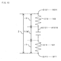
- an impedance Z of the given surface side electrode 01X to 16X-detection portion A0101 to A 1616-back side electrode 0 1 Y to 16Y is constituted by an electric resistance rX of the surface side electrode 01X to 16X from the surface side connection portion 01X1 to 16X1 to the detection portion A0101 to A1616, a capacitive reactance 1/ ⁇ C of the detection portion A0101 to A1616, and an electric resistance rY of the back side electrode 01Y to 16Y from the back side connection portion 01Y1 to 16Y1 to the detection portion A0101 1 to A1616.
- the impedance Z of the given surface side electrode 01X to 16X-detection portion A0101 to A1616-back side electrode 01Y to 16Y and a displacement angle (phase) ⁇ of a current relative to a voltage are input into the calculation portion 3 from the sensor main body 2.
- the measurement subject is placed on the sensor main body 2, whereupon the electrostatic capacity C is calculated in relation to each of the detection portions A0101 to A1616 using the electrostatic capacity calculation method described above in a similar manner to the calculation performed prior to placement of the measurement subject.
- the electrostatic capacity C is calculated in a scan-like manner from the detection portion A0101 to the detection portion A1616.
- the calculated electrostatic capacity C is stored in the RAM 32 in relation to each of the detection portions A0101 to A1616.
- the CPU 31 calculates the surface pressure applied to the sensor main body 2 from a variation ⁇ C in the electrostatic capacity C before and after placement of the measurement subject. More specifically, a map indicating correspondence between the electrostatic capacity C and the surface pressure is stored in the ROM 33 in advance. The surface pressure of a given detection portion A0101 to A1616 is then calculated by substituting the electrostatic capacity C into the map. The surface pressure is then displayed on the screen of the display 34 in relation to each of the detection portions A0101 to A1616.
- the surface side electrodes 01X to 16X and the back side electrodes 01Y to 16Y both take a belt shape.
- the detection portions A0101 to A1616 are arranged using the intersecting portions between the surface side electrodes 01X to 16X and the back side electrodes 01Y to 16Y.
- the number of arranged electrodes is reduced.
- the number of arranged conductors is also reduced. More specifically, a total of 256 detection portions A0101 to A161616 are arranged on the sensor main body 2. When an electrode is arranged for each detection portion A0101 to A161616, 256 surface side electrodes and 256 back side electrodes are required.
- the surface side electrodes 01X to 16X and the back side electrodes 01 Y to 16Y are formed to include acrylic rubber and conductive carbon black.
- the surface side electrodes 01X to 16X and the back side electrodes 01Y to 16Y are both expandable and contractible together with the dielectric layer 20 in accordance with the load. Therefore, expansion and contraction of the dielectric layer 20 is unlikely to be restricted by the surface side electrodes 0 1 X to 16X or the back side electrodes 0 1 Y to 16Y.
- the surface side conductors 01x to 16x and the back side conductors 01y to 16y are formed to include urethane rubber and silver powder. Hence, when a load is applied by the measurement subject, the surface side conductors 01x to 16x and the back side conductors 01y to 16y can expand and contract in accordance with the load. Therefore, expansion and contraction of the dielectric layer 20 is unlikely to be restricted by the surface side conductors 01x to 16x or the back side conductors 01y to 16y.
- the electric resistance rX from the surface side connection portions 01X1 to 16X1 to the detection portions A0101 to A1616 and the electric resistance rY from the back side connection portions 01Y1 to 16Y1 to the detection portions A0101 to A1616 are separated from the impedance Z.
- the electrostatic capacity C of the detection portions A0101 to A1616 is extracted from the impedance Z. Therefore, the measurement precision of the surface pressure distribution is high.
- the calculation portion 3 can calculate the total load applied to the sensor main body 2 by integrating the variation ⁇ C in the electrostatic capacity C of the detection portions A0101 to A1616. Hence, the weight of the measurement subject can be detected.
- the surface side electrodes 01X to 16X are arranged at substantially equal intervals in the X direction and the Y direction over the entire surface of the sensor main body 2.
- the back side electrodes 01Y to 16Y are arranged at substantially equal intervals in the X direction and the Y direction over the entire surface of the sensor main body 2.
- the surface side electrodes 01X to 16X and the back side electrodes 01Y to 16Y are arranged to be substantially orthogonal to each other when seen from the up-down direction.
- the detection portions A0101 to A1616 can be dispersed over the entire surface of the sensor main body 2.
- the surface area of portions in which the surface pressure is detected can be increased.
- the surface side electrodes 01X to 16X, the surface side conductors 01x to 16x, the back side electrodes 01Y to 16Y, and the back side conductors 01y to 16y are arranged on the dielectric layer 20 using a screen printing method. Therefore, the constitutional elements required for surface pressure measurement can be integrated in a comparatively simple manner. As a result, the production efficiency of the sensor main body 2, and therefore the capacitive sensor 1, is high.
- the capacitive sensor 1 is provided with the surface side insulating cover layer 21 and the back side insulating cover layer 22. Hence, conduction from the surface side electrodes 01X to 16X and the surface side conductors 01x to 16x to a member outside the capacitive sensor 1 can be suppressed. Likewise, conduction from the back side electrodes 01Y to 16Y and the back side conductors 01y to 16y to a member outside the capacitive sensor 1 can be suppressed.
- the blended amount (critical volume fraction: ⁇ c) of conductive carbon black at a first polarity change point, at which the electric resistance decreases to cause a transition between insulator and conductor in a percolation curve expressing a relationship between the electric resistance and the blended amount of conductive carbon black in the elastomer composition forming the surface side electrodes 01X to 16X and the back side electrodes 01Y to 16Y of the capacitive sensor 1 according to this embodiment is approximately 4vol%. Therefore, the conductive carbon black forms an aggregate easily. Hence, the surface side electrodes 01X to 16X and the back side electrodes 01Y to 16Y having favorable conductivity can be obtained with a comparatively small amount of conductive carbon black.
- a total of 16 surface side electrodes 01X to 16X are printed onto an inner surface of the surface side insulating sheet 250.
- a total of 16 back side electrodes 16Y are printed onto an inner surface of the back side insulating sheet 251.
- the dielectric layer 20 is interposed between the surface side electrodes 01X to 16X and the back side electrodes 16Y inside the insulating tube member 25.
- the surface side conductors are then dried.
- the back side electrode printing step the back side electrodes 16Y are printed onto the inner surface of the back side insulating sheet 251 using a screen printer.
- the back side electrodes 16Y are then vulcanized.
- the back side conductor printing step the back side conductors are printed onto the inner surface of the back side insulating sheet 251 using a screen printer.
- the back side conductors are then dried.
- the insulating tube member manufacturing step the surface side insulating sheet 250 and the back side insulating sheet 251 are adhered to each other. Thus, the insulating tube member 25 is manufactured.
- the dielectric layer insertion step the dielectric layer 20 is inserted into the interior of the insulating tube member 25.
- the capacitive sensor 1 according to this embodiment exhibits similar advantageous effects to the capacitive sensor of the third embodiment.
- the capacitive sensor 1 of this embodiment printing is not performed directly onto the dielectric layer 20. Therefore, a material that is not suitable for printing (such as a foam body, for example) can be used as the dielectric layer 20. Hence, the freedom of material selection of the dielectric layer 20 is improved.
- the constitutional elements required for surface pressure measurement namely the dielectric layer 20, the surface side electrodes 01X to 16X, the surface side conductors, the back side electrodes 16Y, and the back side conductors, are accommodated inside the insulating tube member 25. Hence, conduction between these members and a member outside the insulating tube member 25 can be suppressed.
- Embodiments of the second capacitive sensor according to the present invention are described above. However, the embodiments are not limited to the above embodiments, and various modified and improved embodiments may be implemented by a person skilled in the art.
- the electrostatic capacity C before the measurement subject is placed and the electrostatic capacity C after the measurement subject is placed are calculated, whereupon the surface pressure distribution is determined from the variation ⁇ C in the electrostatic capacity.
- a surface pressure before the placement may be determined from the electrostatic capacity C before the placement of the measurement subject
- a surface pressure after the placement may be determined from the electrostatic capacity C after the placement of the measurement subject
- the surface pressure distribution may be determined from variation in the surface pressure.
- the capacitive sensor 1 may be used as a seating position detection sensor for a vehicle seat, a touch sensor, a user position detection sensor or the like in an electric carpet, and so on.
- the sensor main body 2 of the capacitive sensor 1 contains an elastomer, and is therefore particularly flexible. Hence, a user does not feel much discomfort even when the capacitive sensor 1 is arranged comparatively close to the body of the user. Accordingly, the capacitive sensor 1 is particularly suitable for detecting a load from a human being (bodyweight, for example). Further, a personal computer may be used as the calculation portion 3.
- the manufacturing method for the capacitive sensor 1 may be executed in order of the surface side conductor printing step to the surface side electrode printing step. Similarly, the manufacturing method may be executed in order of the back side conductor printing step to the back side electrode printing step.
- the elastomer constituting the dielectric layer 20 may be selected appropriately from rubber and thermoplastic elastomers. There are no particular limitations on the elastomer. For example, an elastomer having a large specific dielectric constant is preferable in terms of increasing the capacitance. For example, an elastomer having a specific dielectric constant at room temperature of 3 or more, and more preferably 5 or more, may be employed.
- An elastomer containing a polar functional group such as an ester group, a carboxyl group, a hydroxyl group, a halogen group, an amide group, a sulfone group, a urethane group, or a nitrile group, or an elastomer to which a polar low molecular weight compound containing these polar functional groups is added, for example, may be employed favorably.
- the elastomer may be crosslinked or not crosslinked. Further, by adjusting the Young's modulus of the elastomer, the detection sensitivity and the detection range can be adjusted in accordance with the application.
- the dielectric layer 20 may be selected from the dielectric layers 20 having various Young's moduli in accordance with the load of the measurement subject.
- a foam body is used favorably as the elastomer of the dielectric layer 20. This is because the Young's modulus of a foam body is small, and therefore the dielectric layer 20 deforms sufficiently even when the load of the measurement subject is small. In other words, this is because the surface pressure and the load of the measurement subject can be detected reliably.
- Examples of preferred elastomers include silicone rubber, acrylonitrile-butadiene copolymer rubber, acrylic rubber, epichlorohydrin rubber, chlorosulfonated polyethylene, chlorinated polyethylene, and urethane rubber.
- the thickness of the dielectric layer 20 is preferably set at 1 ⁇ m or more and 3000 ⁇ m or less from the viewpoints of reducing the size of the sensor main body 2 and improving the detection sensitivity by increasing the electrostatic capacity C in proportion to the inverse of the thickness of the dielectric layer 20 (i.e. the distance between electrodes d), as shown by Equation (1).
- a thickness of 50 ⁇ m or more and 500 ⁇ m or less is more preferable.
- the elastomer constituting the surface side electrodes 01X to 16X and the back side electrodes 01Y to 16Y may be the same as the elastomer used for the dielectric layer 20 or may be different.
- the surface side electrodes 01X to 16X, the back side electrodes 01Y to 16Y, and the dielectric layer 20 are constituted by the identical elastomer, the ability of the surface side electrodes 01X to 16X and the back side electrodes 01 Y to 16Y to follow deformation of the dielectric layer 20 is improved.
- the average particle diameter (primary particle) of the conductive fillers is preferably 0.01 ⁇ m or more and 0.5 ⁇ m or less.
- the average particle diameter is preferably 0.03 ⁇ m or more.
- the average particle diameter is preferably 0.1 ⁇ m or less.
- the filling rate of the conductive fillers is preferably set at 25vol% or less when the volume of the surface side electrodes 01X to 16X and the back side electrodes O 1 Y to 16Y is 100vol%, and more preferably at 15vol% or less.
- the thickness of the surface side electrodes 01X to 16X and the back side electrodes 01Y to 16Y is preferably set at 1 ⁇ m or more and 100 ⁇ m or less, taking into consideration the ability of the surface side electrodes 01X to 16X and the back side electrodes 01Y to 16Y to follow the dielectric layer 20 and in order to reduce the size of the sensor main body 2.
- Young's modulus of the surface side electrodes 01X to 16X and the back side electrodes 01Y to 16Y is preferably 0.1 MPa or more and 10 MPa or less to improve the ability of the surface side electrodes 01X to 16X and the back side electrodes 0 1 Y to 16Y to follow deformation of the dielectric layer 20.
- elongation at break in the tensile test JIS K6251
- JIS K6251 elongation at break in the tensile test
- the electric resistance of the surface side electrodes 01X to 16X and the back side electrodes 0 1 Y to 16Y is preferably 100 k ⁇ or less and more preferably 10 k ⁇ or less in the thickness direction and the surface direction.
- variation in the conductivity of the surface side electrodes 01X to 16X and the back side electrodes 01 Y to 16Y remains small even during expansion and contraction.
- the elastomer constituting the surface side conductors 01x to 16x and the back side conductors 01y to 16y may be the same as the elastomer used for the dielectric layer 20, the surface side electrodes 01X to 16X, and the back side electrodes 0 1 Y to 16Y or may be different.
- Suitable examples of the elastomer include silicone rubber, ethylene-propylene copolymer rubber, natural rubber, styrene-butadiene copolymer rubber, acrylonitrile-butadiene copolymer rubber, acrylic rubber, epichlorohydrin rubber, chlorosulfonated polyethylene, chlorinated polyethylene, and urethane rubber.
- the type of conductive particles as long as the conductivity thereof is high.
- metal powder made of silver, gold, copper, nickel, and so on may be employed.
- the filling rate of the conductive particles in the elastomer is preferably set at 20vol% or more when the volume of the surface side conductors 01x to 16x and the back side conductors 01y to 16y is 100vol%.
- the filling rate of the conductive particles in the elastomer is preferably 50vol% or less so as to suppress reductions in the stretchability of the surface side conductors 01x to 16x and the back side conductors 01y to 16y.
- a sheet made of acrylic rubber, urethane rubber, silicone rubber, ethylene-propylene copolymer rubber, natural rubber, styrene-butadiene rubber, acrylonitrile-butadiene rubber, epichlorohydrin rubber, chlorosulfonated polyethylene, chlorinated polyethylene, and so on may be used as the material for forming the surface side insulating cover layer 21, the back side insulating cover layer 22, and the insulating tube member 25.
- a manufacturing method for the capacitive sensor 4 will be described. First, the electrode coating, the conductor coating, and the cover film coating were respectively prepared.
- the coatings described above were respectively printed onto the surface and the back of the urethane rubber sheet in sequence.
- a table sliding semiautomatic printing machine (“SSA-PC660IP”, manufactured by Tokai Seiki Co., Ltd.) was used for printing.
- a conductor plate and the urethane rubber sheet were set on the printing machine.
- the conductor coating was then placed on the conductor plate, whereupon a squeegee was moved on the plate in a scan-like manner to print a conductor on the surface of the urethane rubber sheet.
- the urethane rubber sheet was then left in a drying oven at approximately 140°C for approximately 20 minutes in order to dry the urethane rubber sheet and advance the crosslinking reaction.
- an electrode plate and the urethane rubber sheet on which the conductor was formed were set on the printing machine.
- the electrode coating was then placed on the plate, whereupon the squeegee was moved on the plate in a scan-like manner to print an electrode on the surface of the urethane rubber sheet.
- the urethane rubber sheet was then left in a drying oven at approximately 150°C for approximately 30 minutes in order to dry the urethane rubber sheet and advance the crosslinking reaction.
- a cover film plate and the urethane rubber sheet on which the conductor and the electrode were formed were set on the printing machine.
- the cover film coating was then placed on the plate, whereupon the squeegee was moved on the plate in a scan-like manner to print a cover film on the surface of the urethane rubber sheet.
- the urethane rubber sheet was then left in a drying oven at approximately 150°C for approximately 30 minutes in order to dry the urethane rubber sheet and advance the crosslinking reaction.
- the conductor and the electrode were formed on the surface of the urethane rubber sheet and the cover film was formed on the same surface so as to cover the conductor and the electrode.
- the conductor and the electrode were then formed similarly on the back of the urethane rubber sheet, whereupon the cover film was formed on the same surface so as to cover the conductor and the electrode.
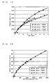
- FIG 13 shows capacitance variation relative to a deformation ratio.
- the deformation ratio is a ratio (a/a 0 ) of a length a of the electrode after elongation in the longitudinal direction (elongation direction) to an initial length a 0 of the electrode.
- the capacitance increased linearly relative to the deformation ratio.
- the capacitance increased as the elongation amount increased.
- the conductors and the electrodes were not disconnected even when the sensor unit was elongated to the deformation ratio of 1.5 (by approximately 50%). It was therefore confirmed that the capacitive sensor according to the present invention possesses stretchability and can detect deformation accurately.
- the surface area of the portions of the sensor main body 2 in which the surface side electrodes 0 1 X to 16X and the back side electrodes 0 1 Y to 16Y were arranged was set at 552 cm 2 .
- a weight pressing the sensor main body 2 had a rectangular parallelepiped shape.
- the surface area of the weight pressing the sensor main body 2 (a load application surface area) was set at 324 cm 2 , 180 cm 2 , and 149 cm 2 . Variation in the electrostatic capacity obtained from the detection portions A0101 to A1616 when the load was increased in each of three patterns of the load application surface area was then observed.
- FIG 14 is a graph showing a relationship between a load and an integrated value of electrostatic capacity.
- the total load applied to the sensor main body 2 by the weight is proportional to the integrated value of electrostatic capacity.
- FIG. 15 is a graph showing a relationship between the surface pressure and the electrostatic capacity.
- the electrostatic capacity distribution corresponds to the shape (substantially square) of the load application surface of the weight.
Landscapes
- Engineering & Computer Science (AREA)
- Physics & Mathematics (AREA)
- General Physics & Mathematics (AREA)
- General Engineering & Computer Science (AREA)
- Theoretical Computer Science (AREA)
- Power Engineering (AREA)
- Human Computer Interaction (AREA)
- Chemical & Material Sciences (AREA)
- Analytical Chemistry (AREA)
- Force Measurement Appropriate To Specific Purposes (AREA)
- Measurement Of Length, Angles, Or The Like Using Electric Or Magnetic Means (AREA)
Claims (7)
- Kapazitiver Sensor, aufweisend eine dielektrische Schicht (40), die aus einem Elastomer besteht, und ein Paar Elektroden (41a, 41b), die über die dielektrische Schicht (40) angeordnet sind, wobei der kapazitive Sensor eine Verformung auf Basis einer Variation der elektrostatischen Kapazität zwischen dem Paar Elektroden (41 a, 41 b) erfasst,
dadurch gekennzeichnet, dass
die dielektrische Schicht (40) expandierbar und zusammenziehbar ist,
das Paar Elektroden (41a, 41b) ein Elastomer und leitende Füller enthalten, die in das Elastomer gefüllt werden, in Übereinstimmung mit einer Verformung der dielektrischen Schicht (40) expandierbar und zusammenziehbar sind, und einen elektrischen Widerstand über Anschlüsse aufweisen, wenn die Elektroden (41a, 41b) zu 100 % in einer Richtung verlängert sind, der im Verhältnis zu einem elektrischen Widerstand über die Anschlüsse vor der Verlängerung höchstens das zehnfache beträgt,
zumindest die dielektrische Schicht (40) und/oder die Elektroden (41 a, 41b) durch ein Druckverfahren ausgebildet werden, bei dem eine dielektrische Schichtbeschichtung, die eine Bildungskomponente der dielektrischen Schicht (40) enthält oder eine Elektrodenbeschichtung, die eine Bildungskomponente der Elektrode (41 a, 41 b) enthält, verwendet werden, und
der gesamte kapazitive Sensor dehnbar ist. - Kapazitiver Sensor nach Anspruch 1, ferner aufweisend dehnbare Leiter (42a, 42b), die mit einer entsprechenden Elektrode des Paars Elektroden (41a, 41b) verbunden sind, wobei jeder der Leiter (42a, 42b) ein Elastomer und leitende Partikel enthält, die in das Elastomer gefüllt sind, einen niedrigeren elektrischen Widerstand als den elektrischen Widerstand der Elektroden (41a, 41b) aufweist und durch das Druckverfahren ausgebildet wird, bei dem eine Leiterbeschichtung verwendet wird, die eine Bildungskomponente des Leiters (42a, 42b) enthält.
- Kapazitiver Sensor nach Anspruch 2, wobei das Paar Elektroden (41a, 41b) und die Leiter (42a, 42b) auf eine Oberfläche und eine Rückseite der dielektrischen Schicht (40) gedruckt sind.
- Kapazitiver Sensor nach Anspruch 2, ferner aufweisend eine Isolationsschicht (43a, 43b), die so angeordnet ist, dass sie zumindest eine der Elektroden (41a, 41b) und/oder den entsprechenden Leiter (42a, 42b) bedeckt, um die Elektrode (41a, 41b) und den Leiter (42a, 42b) von außen zu isolieren.
- Kapazitiver Sensor nach Anspruch 2, ferner aufweisend ein Paar elastischer Substrate (53a, 53b), die über die dielektrische Schicht (50) angeordnet sind, wobei
die Elektrode (51a), die eine Oberfläche der dielektrischen Schicht (50) berührt, und der entsprechende Leiter (52a) auf eine Rückseite eines der elastischen Substrate (53a) gedruckt sind, und
die Elektrode (51b), die eine Rückseite der dielektrischen Schicht (50) berührt, und der entsprechende Leiter (52b) auf eine Oberfläche des anderen elastischen Substrats (53b) gedruckt sind. - Kapazitiver Sensor nach Anspruch 1, wobei
das Paar Elektroden (41a, 41b) aus einem Elastomergemisch besteht, die das Elastomer (101) und die leitenden Füller (102) enthält, und
in einer Perkolationskurve, die ein Verhältnis zwischen einer Mischmenge der leitenden Füller (102) und einem elektrischen Widerstand in dem Elastomergemisch widergibt, die Mischmenge (kritischer Mengenanteil: φc) der leitenden Füller (102) an einem ersten Polaritäts-Wechselpunkt, an dem sich der elektrische Widerstand verringert, um einen Übergang zwischen dem Isolator und Leiter zu verursachen, 25 vol% oder weniger beträgt. - Kapazitiver Sensor nach Anspruch 1, wobei die leitenden Füller, aus denen das Paar Elektroden (41a, 41b) besteht, aus einem Kohlenstoffmaterial bestehen.
Priority Applications (1)
| Application Number | Priority Date | Filing Date | Title |
|---|---|---|---|
| EP12182416.3A EP2549252B8 (de) | 2008-08-08 | 2009-08-06 | Kapazitiver Sensor |
Applications Claiming Priority (2)
| Application Number | Priority Date | Filing Date | Title |
|---|---|---|---|
| JP2008206410A JP4650538B2 (ja) | 2008-08-08 | 2008-08-08 | 静電容量型センサ |
| JP2008206413A JP4565359B2 (ja) | 2008-08-08 | 2008-08-08 | 静電容量型面圧分布センサ |
Related Child Applications (2)
| Application Number | Title | Priority Date | Filing Date |
|---|---|---|---|
| EP12182416.3A Division EP2549252B8 (de) | 2008-08-08 | 2009-08-06 | Kapazitiver Sensor |
| EP12182416.3A Division-Into EP2549252B8 (de) | 2008-08-08 | 2009-08-06 | Kapazitiver Sensor |
Publications (3)
| Publication Number | Publication Date |
|---|---|
| EP2154503A2 EP2154503A2 (de) | 2010-02-17 |
| EP2154503A3 EP2154503A3 (de) | 2012-03-07 |
| EP2154503B1 true EP2154503B1 (de) | 2014-10-22 |
Family
ID=41268417
Family Applications (2)
| Application Number | Title | Priority Date | Filing Date |
|---|---|---|---|
| EP12182416.3A Active EP2549252B8 (de) | 2008-08-08 | 2009-08-06 | Kapazitiver Sensor |
| EP09010183.3A Active EP2154503B1 (de) | 2008-08-08 | 2009-08-06 | Kapazitiver Verformungssensor |
Family Applications Before (1)
| Application Number | Title | Priority Date | Filing Date |
|---|---|---|---|
| EP12182416.3A Active EP2549252B8 (de) | 2008-08-08 | 2009-08-06 | Kapazitiver Sensor |
Country Status (2)
| Country | Link |
|---|---|
| US (1) | US7958789B2 (de) |
| EP (2) | EP2549252B8 (de) |
Cited By (1)
| Publication number | Priority date | Publication date | Assignee | Title |
|---|---|---|---|---|
| WO2017057598A1 (ja) * | 2015-09-30 | 2017-04-06 | 住友理工株式会社 | 静電容量型センサ |
Families Citing this family (96)
| Publication number | Priority date | Publication date | Assignee | Title |
|---|---|---|---|---|
| WO2009006318A1 (en) | 2007-06-29 | 2009-01-08 | Artificial Muscle, Inc. | Electroactive polymer transducers for sensory feedback applications |
| US9383281B2 (en) * | 2009-02-19 | 2016-07-05 | Ford Motor Company | Fuel storage system and method for detecting a gas pressure therein |
| US8866500B2 (en) | 2009-03-26 | 2014-10-21 | Cypress Semiconductor Corporation | Multi-functional capacitance sensing circuit with a current conveyor |
| US8915151B2 (en) * | 2009-06-05 | 2014-12-23 | Sungkyunkwan University Foundation For Corporate Collaboration | Active skin for conformable tactile interface |
| DE102010010348A1 (de) * | 2010-03-05 | 2011-09-08 | Albert-Ludwigs-Universität Freiburg | Implantierbare Vorrichtung zum Erfassen einer Gefäßwanddehnung |
| WO2011145411A1 (ja) * | 2010-05-19 | 2011-11-24 | 東海ゴム工業株式会社 | 導電膜、およびそれを用いたトランスデューサ、フレキシブル配線板 |
| JP5551012B2 (ja) | 2010-07-29 | 2014-07-16 | 東海ゴム工業株式会社 | 配線体接続構造体 |
| KR20140026322A (ko) | 2010-08-23 | 2014-03-05 | 사이프레스 세미컨덕터 코포레이션 | 상호 커패시턴스 감지 회로들, 방법들 및 시스템들 |
| US20120042943A1 (en) * | 2010-08-23 | 2012-02-23 | Du Pont Apollo Limited | Backsheet for a photovoltaic module |
| US9013441B2 (en) | 2010-08-24 | 2015-04-21 | Cypress Semiconductor Corporation | Smart scanning for a capacitive sensing array |
| US9285902B1 (en) | 2010-08-25 | 2016-03-15 | Parade Technologies, Ltd. | Multi-phase scanning |
| US8552746B2 (en) | 2010-12-22 | 2013-10-08 | Visteon Global Technologies, Inc. | Proximity sensor including a multilayer elastomer assembly |
| WO2012118916A2 (en) | 2011-03-01 | 2012-09-07 | Bayer Materialscience Ag | Automated manufacturing processes for producing deformable polymer devices and films |
| US8729911B2 (en) | 2011-04-19 | 2014-05-20 | Cypress Semiconductor Corporation | Usage of weighting matrices in multi-phase scanning modes |
| US11320946B2 (en) * | 2011-04-19 | 2022-05-03 | Cypress Semiconductor Corporation | Capacitive panel scanning with reduced number of sensing circuits |
| FR2976110B1 (fr) * | 2011-05-30 | 2014-01-17 | Commissariat Energie Atomique | Dispositif d'affichage a surface deformable et a capteurs de position |
| WO2013005432A1 (ja) | 2011-07-04 | 2013-01-10 | 東海ゴム工業株式会社 | 外部操作の検出構造体 |
| US20140035603A1 (en) * | 2012-08-03 | 2014-02-06 | Xerox Corporation | Printed Stretch Sensor |
| JP5780643B2 (ja) * | 2011-07-28 | 2015-09-16 | 住友理工株式会社 | マットレス |
| JP5719725B2 (ja) | 2011-08-29 | 2015-05-20 | 住友理工株式会社 | クッション用セルとそれを用いたクッション体 |
| WO2013063034A1 (en) * | 2011-10-25 | 2013-05-02 | Unipixel Displays, Inc. | Method of manufacturing a resistive touch sensor circuit by flexographic printing |
| TW201332782A (zh) * | 2011-10-25 | 2013-08-16 | Unipixel Displays Inc | 使用膠版輪轉式印刷之製造電容式觸控感測電路之方法 |
| JP2013104847A (ja) * | 2011-11-16 | 2013-05-30 | Nitto Denko Corp | フィルムセンサ |
| WO2013110846A1 (en) * | 2012-01-26 | 2013-08-01 | Nokia Corporation | Capacitive eye tracking sensor |
| WO2013142552A1 (en) | 2012-03-21 | 2013-09-26 | Bayer Materialscience Ag | Roll-to-roll manufacturing processes for producing self-healing electroactive polymer devices |
| JP6030841B2 (ja) * | 2012-03-26 | 2016-11-24 | 住友理工株式会社 | 静電容量型センサ |
| JP5876358B2 (ja) | 2012-03-30 | 2016-03-02 | 国立大学法人九州大学 | 歩行運動補助具 |
| TW201403899A (zh) | 2012-04-12 | 2014-01-16 | Bayer Materialscience Ag | 具有改良性能之eap傳感器 |
| KR20150031285A (ko) | 2012-06-18 | 2015-03-23 | 바이엘 인텔렉쳐 프로퍼티 게엠베하 | 연신 공정을 위한 연신 프레임 |
| DE102012210277B3 (de) * | 2012-06-19 | 2013-08-22 | Behr-Hella Thermocontrol Gmbh | Kapazitiver Sensor zur Erfassung der Bewegung eines Objekts |
| JP5986445B2 (ja) | 2012-07-20 | 2016-09-06 | 国立大学法人九州大学 | 歩行用遊脚振子運動補助具およびアシスト力の制御方法 |
| WO2014028371A1 (en) * | 2012-08-17 | 2014-02-20 | The Procter & Gamble Company | A monitoring device for monitoring cleaning activity |
| US9250143B2 (en) * | 2012-09-19 | 2016-02-02 | College Park Industries, Inc. | Multicapacitor force/moment sensor arrays |
| JP5497222B2 (ja) * | 2012-09-28 | 2014-05-21 | バンドー化学株式会社 | 静電容量型センサシート及び静電容量型センサシートの製造方法 |
| US9590193B2 (en) * | 2012-10-24 | 2017-03-07 | Parker-Hannifin Corporation | Polymer diode |
| US9380979B2 (en) * | 2012-11-02 | 2016-07-05 | Nokia Technologies Oy | Apparatus and method of assembling an apparatus for sensing pressure |
| WO2014072869A1 (en) * | 2012-11-06 | 2014-05-15 | Koninklijke Philips N.V. | Sensor for moving equipment |
| CN103836864B (zh) * | 2012-11-20 | 2016-08-17 | Lg电子株式会社 | 冰箱 |
| US20140246226A1 (en) * | 2013-03-04 | 2014-09-04 | Uni-Pixel Displays, Inc. | Method of fabricating copper-nickel micro mesh conductors |
| FR3003030B1 (fr) * | 2013-03-11 | 2015-04-17 | Commissariat Energie Atomique | Dispositif de detection de contrainte mecanique a capteur capacitif, ensemble de dispositifs de detection et dispositif de localisation de toucher a capteurs capacitifs |
| FR3003029A1 (fr) * | 2013-03-11 | 2014-09-12 | Commissariat Energie Atomique | Capteur capacitif de contrainte mecanique, ensemble de capteurs et dispositif de localisation de toucher a capteurs capacitifs |
| KR101956105B1 (ko) * | 2013-03-18 | 2019-03-13 | 삼성전자주식회사 | 촉각 측정 장치 및 방법과 촉각 측정 장치 제조 방법 |
| WO2014157627A1 (ja) * | 2013-03-29 | 2014-10-02 | バンドー化学株式会社 | 静電容量型センサシート及び静電容量型センサ |
| US8860682B1 (en) | 2013-04-22 | 2014-10-14 | Cypress Semiconductor Corporation | Hardware de-convolution block for multi-phase scanning |
| US8941392B1 (en) * | 2013-08-17 | 2015-01-27 | Bend Labs, Inc. | Angular displacement sensor of compliant material |
| JP2015045623A (ja) * | 2013-08-29 | 2015-03-12 | バンドー化学株式会社 | 静電容量型センサシート及び静電容量型センサ |
| US9816800B2 (en) | 2013-10-10 | 2017-11-14 | Stretchsense Limited | Method of fabrication of laminates of elastic material suitable for dielectric elastomer sensing |
| KR20150052668A (ko) * | 2013-11-06 | 2015-05-14 | 삼성전자주식회사 | 탄성 고분자 물질의 패터닝 방법 |
| DE102013226880A1 (de) * | 2013-12-20 | 2015-06-25 | BSH Hausgeräte GmbH | Haushaltsgerät zur Pflege von Wäschestücken und Verfahren zum Erfassen einer Bewegung eines Laugenbehälters |
| DE102014201434B4 (de) | 2014-01-27 | 2016-10-13 | Fraunhofer-Gesellschaft zur Förderung der angewandten Forschung e.V. | Volumenkompressible kapazitive flächige flexible Sensormatte zur Messung von Druck oder Druckverteilungen und/oder zur Messung oder Detektion von Deformationen |
| JPWO2015133417A1 (ja) * | 2014-03-03 | 2017-04-06 | バンドー化学株式会社 | センサ装置及び伸縮構造体 |
| US9766171B2 (en) * | 2014-03-17 | 2017-09-19 | Columbia Insurance Company | Devices, systems and method for flooring performance testing |
| EP3130287B1 (de) * | 2014-04-09 | 2022-05-11 | Bando Chemical Industries, Ltd. | Sensorvorrichtung |
| US20150370372A1 (en) * | 2014-06-20 | 2015-12-24 | Maxim Integrated Products, Inc. | Capacitive touch panel having dielectric structures formed therein |
| DE102014117991B4 (de) * | 2014-12-05 | 2018-03-22 | Preh Gmbh | Kapazitiver Kraftsensor |
| EP3236225A4 (de) * | 2014-12-18 | 2018-07-18 | Nitta Corporation | Sensorfolie |
| DE102015105004B3 (de) * | 2015-03-31 | 2016-09-01 | Fraunhofer-Gesellschaft zur Förderung der angewandten Forschung e.V. | Textilmaterial mit eingearbeiteten Elastomersensoren |
| WO2016155887A1 (de) * | 2015-04-02 | 2016-10-06 | Bauer Jörg R | Touchpad und system zum erfassen eines gegenstandes auf einer erfassungsfläche sowie erzeugen und ausgeben gegenstandsspezifischer information |
| US9612102B2 (en) | 2015-04-17 | 2017-04-04 | Bend Labs, Inc | Compliant multi-region angular displacement and strain sensors |
| TWI575232B (zh) | 2015-06-12 | 2017-03-21 | 財團法人工業技術研究院 | 感測裝置 |
| WO2017022258A1 (ja) | 2015-07-31 | 2017-02-09 | 住友理工株式会社 | 静電容量型センサ、センサシートおよび静電容量型センサの製造方法 |
| KR101731173B1 (ko) * | 2015-09-02 | 2017-04-28 | 한국과학기술원 | 다공성 탄성중합체 유전층을 구비하는 정전용량형 압력센서 |
| CN108139834B (zh) * | 2015-10-13 | 2020-12-29 | 阿尔卑斯阿尔派株式会社 | 输入装置以及输入装置的制造方法 |
| US9891739B2 (en) | 2016-02-29 | 2018-02-13 | Microsoft Technology Licensing, Llc | Deformable touch and strain sensor |
| DE202016001419U1 (de) * | 2016-03-07 | 2017-06-12 | I.G. Bauerhin Gmbh | Kapazitiver Flächensensor |
| US10054503B2 (en) | 2016-03-11 | 2018-08-21 | Microsoft Technology Licensing, Llc | Force sensor |
| US10959644B2 (en) | 2016-03-24 | 2021-03-30 | Bend Labs Inc. | Compliant sensors for force sensing |
| KR102553036B1 (ko) * | 2016-06-29 | 2023-07-07 | 엘지이노텍 주식회사 | 압력 감지 센서 |
| FI127245B (en) * | 2016-07-11 | 2018-02-15 | Forciot Oy | Force and / or pressure sensor |
| US10602989B2 (en) | 2016-09-02 | 2020-03-31 | Canon U.S.A., Inc. | Capacitive sensing and encoding for imaging probes |
| JP6770743B2 (ja) * | 2016-12-20 | 2020-10-21 | 北川工業株式会社 | 感圧センサー |
| US11892487B2 (en) * | 2017-03-23 | 2024-02-06 | Sensor Holdings Limited | Sensing over a shared physical channel |
| DE102017205251A1 (de) * | 2017-03-28 | 2018-10-04 | B. Braun Melsungen Ag | Medizinische Pumpvorrichtung |
| JP2018189438A (ja) * | 2017-04-28 | 2018-11-29 | 北川工業株式会社 | 感圧センサー |
| US10701987B2 (en) | 2017-08-31 | 2020-07-07 | Nike, Inc. | Sense-enabled apparel |
| KR102103171B1 (ko) * | 2018-08-27 | 2020-06-01 | (주)모어씽즈 | 정전식 센서와 저항식 센서를 통합한 하이브리드 대면적 압력 센서 |
| JP7281630B2 (ja) * | 2018-10-18 | 2023-05-26 | パナソニックIpマネジメント株式会社 | 感圧素子および電子機器 |
| GB2580928B (en) | 2019-01-30 | 2023-02-08 | Hyve Dynamics Holdings Ltd | A stretchable bidirectional capacitive pressure sensor and method of use |
| CN109916292B (zh) * | 2019-02-25 | 2021-05-04 | 武汉工程大学 | 一种多层电容式柔性智能可穿戴传感器件的制备方法 |
| US12278572B2 (en) | 2019-03-04 | 2025-04-15 | The Regents Of The University Of Colorado, A Body Corporate | Composite layering of hydraulically amplified self-healing electrostatic transducers |
| JP6644961B1 (ja) * | 2019-03-28 | 2020-02-12 | 住友理工株式会社 | 静電型トランスデューサおよびその製造方法 |
| DE112020001835T5 (de) * | 2019-04-10 | 2022-01-13 | Iee International Electronics & Engineering S.A. | Mehrkanal-Kapazitäts-Abtastmessschaltung |
| EP3952341B1 (de) | 2019-04-26 | 2024-09-11 | Sumitomo Riko Company Limited | Elektrostatischer wandler und elektrostatische wandlereinheit |
| JP7229095B2 (ja) | 2019-05-16 | 2023-02-27 | Cyberdyne株式会社 | 触力覚検知装置、触力覚検知方法およびロボットアーム |
| CN114502024A (zh) | 2019-05-31 | 2022-05-13 | 耐克创新有限合伙公司 | 自适应支撑服装系统和方法 |
| WO2020258061A1 (zh) * | 2019-06-26 | 2020-12-30 | 百医医材科技股份有限公司 | 压力感应系统及压力感应设定方法 |
| CN111000565A (zh) * | 2019-12-06 | 2020-04-14 | 北京华严互娱科技有限公司 | 一种运动捕捉传感器装置及其制造方法 |
| JP2021156607A (ja) | 2020-03-25 | 2021-10-07 | 株式会社ジャパンディスプレイ | センサ装置及びモジュール |
| WO2022050997A2 (en) * | 2020-05-29 | 2022-03-10 | The Regents Of The University Of Colorado, A Body Corporate | Capacitive self-sensing for electrostatic transducers with high voltage isolation |
| US11827459B2 (en) | 2020-10-16 | 2023-11-28 | Artimus Robotics Inc. | Control of conveyor systems using hydraulically amplified self-healing electrostatic (HASEL) actuators |
| EP4019926A1 (de) * | 2020-12-22 | 2022-06-29 | Max-Planck-Gesellschaft zur Förderung der Wissenschaften e.V. | System und verfahren zur gleichzeitigen erfassung von kontaktkraft und seitlicher belastung |
| JP7487148B2 (ja) | 2021-06-14 | 2024-05-20 | 双葉電子工業株式会社 | 静電容量型圧力センサ |
| CN113892953B (zh) * | 2021-10-09 | 2023-04-14 | 中国人民解放军海军军医大学第一附属医院 | 一种使用柔性传感器的脊柱测压装置 |
| CN116539072B (zh) * | 2022-01-25 | 2026-03-13 | 腾讯科技(深圳)有限公司 | 电容传感器及其制备方法 |
| CN114571503B (zh) * | 2022-02-28 | 2024-07-23 | 深圳市越疆科技有限公司 | 多电极层堆叠式电子皮肤、接近感应方法、机械臂及机器人 |
| CN119321836B (zh) * | 2024-11-01 | 2025-08-15 | 北京大学 | 一种接触主导场增强的柔性电容式压力传感器及制备方法 |
Citations (1)
| Publication number | Priority date | Publication date | Assignee | Title |
|---|---|---|---|---|
| US20050215915A1 (en) * | 2004-03-29 | 2005-09-29 | Sanyo Electric Co., Ltd. | Capacitance-type pressure sensor and heart beat / respiration measuring device using the same |
Family Cites Families (21)
| Publication number | Priority date | Publication date | Assignee | Title |
|---|---|---|---|---|
| JPS5019057A (de) | 1973-06-12 | 1975-02-28 | ||
| JPS61210686A (ja) | 1985-03-15 | 1986-09-18 | Misuzu Erii:Kk | 圧電素子 |
| JPH0652206B2 (ja) | 1986-03-28 | 1994-07-06 | 工業技術院長 | 静電容量型圧力分布測定装置 |
| JPH0353258U (de) | 1989-09-27 | 1991-05-23 | ||
| JPH05288619A (ja) | 1992-04-07 | 1993-11-02 | Youji Yamada | 静電容量式触覚センサ |
| JPH11132879A (ja) | 1997-10-27 | 1999-05-21 | Kanto Bussan Kk | パネル式圧力センサ |
| DE69728577T2 (de) * | 1997-12-31 | 2005-04-28 | Société d'Applications Electroniques pour la Physique, la Science et l'Industrie | Kapazitive sensoren zur messung der feuchtigkeit und deren verfahren zur herstellung |
| JP2001221700A (ja) * | 2000-02-08 | 2001-08-17 | Nitta Ind Corp | 静電容量式センサ |
| US7316167B2 (en) * | 2000-05-16 | 2008-01-08 | Fidelica, Microsystems, Inc. | Method and apparatus for protection of contour sensing devices |
| JP2002340699A (ja) * | 2001-05-21 | 2002-11-27 | Mitsumi Electric Co Ltd | 静電容量センサー |
| US7132642B2 (en) * | 2001-07-09 | 2006-11-07 | Nartron Corporation | Anti-entrapment systems for preventing objects from being entrapped by translating devices |
| US6847527B2 (en) * | 2001-08-24 | 2005-01-25 | 3M Innovative Properties Company | Interconnect module with reduced power distribution impedance |
| JP3983638B2 (ja) | 2002-09-24 | 2007-09-26 | ニッタ株式会社 | センサシート |
| US7317392B2 (en) * | 2004-09-29 | 2008-01-08 | Methode Electronics, Inc. | Apparatus for occupant detection |
| FR2878956A1 (fr) * | 2004-12-03 | 2006-06-09 | Techno Concept Sarl | Procede et dispositif de mesure de distribution de forces a l'aide d'une surface piezo-sensible |
| US7439962B2 (en) * | 2005-06-01 | 2008-10-21 | Synaptics Incorporated | Touch pad with flexible substrate |
| US7395717B2 (en) * | 2006-02-10 | 2008-07-08 | Milliken & Company | Flexible capacitive sensor |
| JP5166714B2 (ja) * | 2006-09-15 | 2013-03-21 | 東海ゴム工業株式会社 | センサー用架橋エラストマー体およびその製法 |
| JP5568206B2 (ja) * | 2006-09-15 | 2014-08-06 | 東海ゴム工業株式会社 | 変形センサ |
| DE602007013162D1 (de) * | 2006-10-25 | 2011-04-28 | Tokai Rubber Ind Ltd | Verformungssensor |
| JP5496446B2 (ja) * | 2007-07-12 | 2014-05-21 | 東海ゴム工業株式会社 | 静電容量型センサ |
-
2009
- 2009-08-04 US US12/535,150 patent/US7958789B2/en active Active
- 2009-08-06 EP EP12182416.3A patent/EP2549252B8/de active Active
- 2009-08-06 EP EP09010183.3A patent/EP2154503B1/de active Active
Patent Citations (1)
| Publication number | Priority date | Publication date | Assignee | Title |
|---|---|---|---|---|
| US20050215915A1 (en) * | 2004-03-29 | 2005-09-29 | Sanyo Electric Co., Ltd. | Capacitance-type pressure sensor and heart beat / respiration measuring device using the same |
Non-Patent Citations (1)
| Title |
|---|
| ASHRUF C M A: "Thin flexible pressure sensors", SENSOR REVIEW, IFS PUBLICATIONS, BEDFORD, GB, vol. 22, no. 4, 1 January 2002 (2002-01-01), pages 322 - 327, XP008147893, ISSN: 0260-2288, DOI: 10.1108102602280210444636 * |
Cited By (1)
| Publication number | Priority date | Publication date | Assignee | Title |
|---|---|---|---|---|
| WO2017057598A1 (ja) * | 2015-09-30 | 2017-04-06 | 住友理工株式会社 | 静電容量型センサ |
Also Published As
| Publication number | Publication date |
|---|---|
| EP2154503A2 (de) | 2010-02-17 |
| EP2154503A3 (de) | 2012-03-07 |
| EP2549252B1 (de) | 2016-09-21 |
| US20100033196A1 (en) | 2010-02-11 |
| US7958789B2 (en) | 2011-06-14 |
| EP2549252A3 (de) | 2014-01-22 |
| EP2549252B8 (de) | 2016-12-21 |
| EP2549252A2 (de) | 2013-01-23 |
Similar Documents
| Publication | Publication Date | Title |
|---|---|---|
| US7958789B2 (en) | Capacitive sensor | |
| JP4650538B2 (ja) | 静電容量型センサ | |
| JP4565359B2 (ja) | 静電容量型面圧分布センサ | |
| JP5622405B2 (ja) | 静電容量型感圧センサおよびその製造方法 | |
| US10317442B2 (en) | Capacitive sensor, sensor sheet, and method for manufacturing capacitive sensor | |
| JP5448423B2 (ja) | 触覚センサおよびその製造方法 | |
| CN104067099B (zh) | 静电电容式传感器 | |
| JP5530798B2 (ja) | 静電容量型センサおよびセンサ取付構造 | |
| JP5496446B2 (ja) | 静電容量型センサ | |
| JP5815369B2 (ja) | 静電容量型センサ | |
| JP5694856B2 (ja) | 柔軟電極構造、および柔軟電極構造を有する電極を備えるトランスデューサ | |
| EP2924406B1 (de) | Lastsensor | |
| KR20170074914A (ko) | 정전 용량형 센서 | |
| JP5486417B2 (ja) | 入力インターフェイス装置 | |
| JP2011075322A (ja) | 静電容量型センサ | |
| JP5465126B2 (ja) | 面圧分布センサ | |
| JP2012163348A (ja) | 静電容量型面状センサ | |
| Heracleous et al. | Scalable 4-D printed tactile sensor for the detection of shear forces in the aid of plantar measurements | |
| Verma et al. | Designing a Highly Sensitive Printed Strain Sensor Array with Microstrain Detection | |
| CN220670773U (zh) | 柔性压力传感器及座椅 | |
| JP2020187053A (ja) | 感圧センサシートおよび感圧センサ |
Legal Events
| Date | Code | Title | Description |
|---|---|---|---|
| PUAI | Public reference made under article 153(3) epc to a published international application that has entered the european phase |
Free format text: ORIGINAL CODE: 0009012 |
|
| AK | Designated contracting states |
Kind code of ref document: A2 Designated state(s): AT BE BG CH CY CZ DE DK EE ES FI FR GB GR HR HU IE IS IT LI LT LU LV MC MK MT NL NO PL PT RO SE SI SK SM TR |
|
| AX | Request for extension of the european patent |
Extension state: AL BA RS |
|
| RIC1 | Information provided on ipc code assigned before grant |
Ipc: B25J 13/08 20060101ALI20111026BHEP Ipc: G01B 7/16 20060101ALI20111026BHEP Ipc: G01D 5/241 20060101ALI20111026BHEP Ipc: G01L 1/14 20060101AFI20111026BHEP Ipc: G01G 7/06 20060101ALI20111026BHEP Ipc: A61B 5/11 20060101ALI20111026BHEP Ipc: G01L 5/22 20060101ALI20111026BHEP Ipc: G06F 3/044 20060101ALI20111026BHEP |
|
| PUAL | Search report despatched |
Free format text: ORIGINAL CODE: 0009013 |
|
| AK | Designated contracting states |
Kind code of ref document: A3 Designated state(s): AT BE BG CH CY CZ DE DK EE ES FI FR GB GR HR HU IE IS IT LI LT LU LV MC MK MT NL NO PL PT RO SE SI SK SM TR |
|
| AX | Request for extension of the european patent |
Extension state: AL BA RS |
|
| RIC1 | Information provided on ipc code assigned before grant |
Ipc: A61B 5/11 20060101ALI20120130BHEP Ipc: G01D 5/241 20060101ALI20120130BHEP Ipc: B25J 13/08 20060101ALI20120130BHEP Ipc: G01G 7/06 20060101ALI20120130BHEP Ipc: G01L 5/22 20060101ALI20120130BHEP Ipc: G01L 1/14 20060101AFI20120130BHEP Ipc: G01B 7/16 20060101ALI20120130BHEP Ipc: G06F 3/044 20060101ALI20120130BHEP |
|
| 17P | Request for examination filed |
Effective date: 20120907 |
|
| GRAP | Despatch of communication of intention to grant a patent |
Free format text: ORIGINAL CODE: EPIDOSNIGR1 |
|
| INTG | Intention to grant announced |
Effective date: 20140527 |
|
| GRAS | Grant fee paid |
Free format text: ORIGINAL CODE: EPIDOSNIGR3 |
|
| GRAA | (expected) grant |
Free format text: ORIGINAL CODE: 0009210 |
|
| AK | Designated contracting states |
Kind code of ref document: B1 Designated state(s): AT BE BG CH CY CZ DE DK EE ES FI FR GB GR HR HU IE IS IT LI LT LU LV MC MK MT NL NO PL PT RO SE SI SK SM TR |
|
| REG | Reference to a national code |
Ref country code: GB Ref legal event code: FG4D |
|
| REG | Reference to a national code |
Ref country code: CH Ref legal event code: EP |
|
| REG | Reference to a national code |
Ref country code: AT Ref legal event code: REF Ref document number: 692872 Country of ref document: AT Kind code of ref document: T Effective date: 20141115 |
|
| REG | Reference to a national code |
Ref country code: IE Ref legal event code: FG4D Ref country code: DE Ref legal event code: R082 Ref document number: 602009027277 Country of ref document: DE Representative=s name: KUHNEN & WACKER PATENT- UND RECHTSANWALTSBUERO, DE |
|
| REG | Reference to a national code |
Ref country code: DE Ref legal event code: R096 Ref document number: 602009027277 Country of ref document: DE Effective date: 20141127 |
|
| RAP2 | Party data changed (patent owner data changed or rights of a patent transferred) |
Owner name: SUMITOMO RIKO COMPANY LIMITED |
|
| REG | Reference to a national code |
Ref country code: DE Ref legal event code: R081 Ref document number: 602009027277 Country of ref document: DE Owner name: SUMITOMO RIKO COMPANY LIMITED, KOMAKI-SHI, JP Free format text: FORMER OWNER: TOKAI RUBBER INDUSTRIES, LTD., KOMAKI-SHI, AICHI-KEN, JP Effective date: 20141119 Ref country code: DE Ref legal event code: R082 Ref document number: 602009027277 Country of ref document: DE Representative=s name: KUHNEN & WACKER PATENT- UND RECHTSANWALTSBUERO, DE Effective date: 20141119 |
|
| REG | Reference to a national code |
Ref country code: NL Ref legal event code: VDEP Effective date: 20141022 |
|
| REG | Reference to a national code |
Ref country code: AT Ref legal event code: MK05 Ref document number: 692872 Country of ref document: AT Kind code of ref document: T Effective date: 20141022 |
|
| REG | Reference to a national code |
Ref country code: LT Ref legal event code: MG4D |
|
| PG25 | Lapsed in a contracting state [announced via postgrant information from national office to epo] |
Ref country code: ES Free format text: LAPSE BECAUSE OF FAILURE TO SUBMIT A TRANSLATION OF THE DESCRIPTION OR TO PAY THE FEE WITHIN THE PRESCRIBED TIME-LIMIT Effective date: 20141022 Ref country code: PT Free format text: LAPSE BECAUSE OF FAILURE TO SUBMIT A TRANSLATION OF THE DESCRIPTION OR TO PAY THE FEE WITHIN THE PRESCRIBED TIME-LIMIT Effective date: 20150223 Ref country code: NO Free format text: LAPSE BECAUSE OF FAILURE TO SUBMIT A TRANSLATION OF THE DESCRIPTION OR TO PAY THE FEE WITHIN THE PRESCRIBED TIME-LIMIT Effective date: 20150122 Ref country code: NL Free format text: LAPSE BECAUSE OF FAILURE TO SUBMIT A TRANSLATION OF THE DESCRIPTION OR TO PAY THE FEE WITHIN THE PRESCRIBED TIME-LIMIT Effective date: 20141022 Ref country code: LT Free format text: LAPSE BECAUSE OF FAILURE TO SUBMIT A TRANSLATION OF THE DESCRIPTION OR TO PAY THE FEE WITHIN THE PRESCRIBED TIME-LIMIT Effective date: 20141022 Ref country code: FI Free format text: LAPSE BECAUSE OF FAILURE TO SUBMIT A TRANSLATION OF THE DESCRIPTION OR TO PAY THE FEE WITHIN THE PRESCRIBED TIME-LIMIT Effective date: 20141022 Ref country code: IS Free format text: LAPSE BECAUSE OF FAILURE TO SUBMIT A TRANSLATION OF THE DESCRIPTION OR TO PAY THE FEE WITHIN THE PRESCRIBED TIME-LIMIT Effective date: 20150222 |
|
| PG25 | Lapsed in a contracting state [announced via postgrant information from national office to epo] |
Ref country code: SE Free format text: LAPSE BECAUSE OF FAILURE TO SUBMIT A TRANSLATION OF THE DESCRIPTION OR TO PAY THE FEE WITHIN THE PRESCRIBED TIME-LIMIT Effective date: 20141022 Ref country code: GR Free format text: LAPSE BECAUSE OF FAILURE TO SUBMIT A TRANSLATION OF THE DESCRIPTION OR TO PAY THE FEE WITHIN THE PRESCRIBED TIME-LIMIT Effective date: 20150123 Ref country code: CY Free format text: LAPSE BECAUSE OF FAILURE TO SUBMIT A TRANSLATION OF THE DESCRIPTION OR TO PAY THE FEE WITHIN THE PRESCRIBED TIME-LIMIT Effective date: 20141022 Ref country code: PL Free format text: LAPSE BECAUSE OF FAILURE TO SUBMIT A TRANSLATION OF THE DESCRIPTION OR TO PAY THE FEE WITHIN THE PRESCRIBED TIME-LIMIT Effective date: 20141022 Ref country code: AT Free format text: LAPSE BECAUSE OF FAILURE TO SUBMIT A TRANSLATION OF THE DESCRIPTION OR TO PAY THE FEE WITHIN THE PRESCRIBED TIME-LIMIT Effective date: 20141022 Ref country code: HR Free format text: LAPSE BECAUSE OF FAILURE TO SUBMIT A TRANSLATION OF THE DESCRIPTION OR TO PAY THE FEE WITHIN THE PRESCRIBED TIME-LIMIT Effective date: 20141022 Ref country code: LV Free format text: LAPSE BECAUSE OF FAILURE TO SUBMIT A TRANSLATION OF THE DESCRIPTION OR TO PAY THE FEE WITHIN THE PRESCRIBED TIME-LIMIT Effective date: 20141022 |
|
| REG | Reference to a national code |
Ref country code: DE Ref legal event code: R097 Ref document number: 602009027277 Country of ref document: DE |
|
| PG25 | Lapsed in a contracting state [announced via postgrant information from national office to epo] |
Ref country code: CZ Free format text: LAPSE BECAUSE OF FAILURE TO SUBMIT A TRANSLATION OF THE DESCRIPTION OR TO PAY THE FEE WITHIN THE PRESCRIBED TIME-LIMIT Effective date: 20141022 Ref country code: RO Free format text: LAPSE BECAUSE OF FAILURE TO SUBMIT A TRANSLATION OF THE DESCRIPTION OR TO PAY THE FEE WITHIN THE PRESCRIBED TIME-LIMIT Effective date: 20141022 Ref country code: SK Free format text: LAPSE BECAUSE OF FAILURE TO SUBMIT A TRANSLATION OF THE DESCRIPTION OR TO PAY THE FEE WITHIN THE PRESCRIBED TIME-LIMIT Effective date: 20141022 Ref country code: EE Free format text: LAPSE BECAUSE OF FAILURE TO SUBMIT A TRANSLATION OF THE DESCRIPTION OR TO PAY THE FEE WITHIN THE PRESCRIBED TIME-LIMIT Effective date: 20141022 Ref country code: DK Free format text: LAPSE BECAUSE OF FAILURE TO SUBMIT A TRANSLATION OF THE DESCRIPTION OR TO PAY THE FEE WITHIN THE PRESCRIBED TIME-LIMIT Effective date: 20141022 |
|
| PLBE | No opposition filed within time limit |
Free format text: ORIGINAL CODE: 0009261 |
|
| STAA | Information on the status of an ep patent application or granted ep patent |
Free format text: STATUS: NO OPPOSITION FILED WITHIN TIME LIMIT |
|
| PG25 | Lapsed in a contracting state [announced via postgrant information from national office to epo] |
Ref country code: IT Free format text: LAPSE BECAUSE OF FAILURE TO SUBMIT A TRANSLATION OF THE DESCRIPTION OR TO PAY THE FEE WITHIN THE PRESCRIBED TIME-LIMIT Effective date: 20141022 |
|
| 26N | No opposition filed |
Effective date: 20150723 |
|
| PG25 | Lapsed in a contracting state [announced via postgrant information from national office to epo] |
Ref country code: SI Free format text: LAPSE BECAUSE OF FAILURE TO SUBMIT A TRANSLATION OF THE DESCRIPTION OR TO PAY THE FEE WITHIN THE PRESCRIBED TIME-LIMIT Effective date: 20141022 |
|
| PG25 | Lapsed in a contracting state [announced via postgrant information from national office to epo] |
Ref country code: LU Free format text: LAPSE BECAUSE OF FAILURE TO SUBMIT A TRANSLATION OF THE DESCRIPTION OR TO PAY THE FEE WITHIN THE PRESCRIBED TIME-LIMIT Effective date: 20150806 Ref country code: MC Free format text: LAPSE BECAUSE OF FAILURE TO SUBMIT A TRANSLATION OF THE DESCRIPTION OR TO PAY THE FEE WITHIN THE PRESCRIBED TIME-LIMIT Effective date: 20141022 |
|
| REG | Reference to a national code |
Ref country code: CH Ref legal event code: PL |
|
| GBPC | Gb: european patent ceased through non-payment of renewal fee |
Effective date: 20150806 |
|
| PG25 | Lapsed in a contracting state [announced via postgrant information from national office to epo] |
Ref country code: LI Free format text: LAPSE BECAUSE OF NON-PAYMENT OF DUE FEES Effective date: 20150831 Ref country code: CH Free format text: LAPSE BECAUSE OF NON-PAYMENT OF DUE FEES Effective date: 20150831 |
|
| REG | Reference to a national code |
Ref country code: IE Ref legal event code: MM4A |
|
| REG | Reference to a national code |
Ref country code: FR Ref legal event code: ST Effective date: 20160429 |
|
| PG25 | Lapsed in a contracting state [announced via postgrant information from national office to epo] |
Ref country code: GB Free format text: LAPSE BECAUSE OF NON-PAYMENT OF DUE FEES Effective date: 20150806 Ref country code: IE Free format text: LAPSE BECAUSE OF NON-PAYMENT OF DUE FEES Effective date: 20150806 |
|
| PG25 | Lapsed in a contracting state [announced via postgrant information from national office to epo] |
Ref country code: FR Free format text: LAPSE BECAUSE OF NON-PAYMENT OF DUE FEES Effective date: 20150831 |
|
| PG25 | Lapsed in a contracting state [announced via postgrant information from national office to epo] |
Ref country code: MT Free format text: LAPSE BECAUSE OF FAILURE TO SUBMIT A TRANSLATION OF THE DESCRIPTION OR TO PAY THE FEE WITHIN THE PRESCRIBED TIME-LIMIT Effective date: 20141022 |
|
| PG25 | Lapsed in a contracting state [announced via postgrant information from national office to epo] |
Ref country code: SM Free format text: LAPSE BECAUSE OF FAILURE TO SUBMIT A TRANSLATION OF THE DESCRIPTION OR TO PAY THE FEE WITHIN THE PRESCRIBED TIME-LIMIT Effective date: 20141022 Ref country code: BG Free format text: LAPSE BECAUSE OF FAILURE TO SUBMIT A TRANSLATION OF THE DESCRIPTION OR TO PAY THE FEE WITHIN THE PRESCRIBED TIME-LIMIT Effective date: 20141022 Ref country code: HU Free format text: LAPSE BECAUSE OF FAILURE TO SUBMIT A TRANSLATION OF THE DESCRIPTION OR TO PAY THE FEE WITHIN THE PRESCRIBED TIME-LIMIT; INVALID AB INITIO Effective date: 20090806 |
|
| PG25 | Lapsed in a contracting state [announced via postgrant information from national office to epo] |
Ref country code: TR Free format text: LAPSE BECAUSE OF FAILURE TO SUBMIT A TRANSLATION OF THE DESCRIPTION OR TO PAY THE FEE WITHIN THE PRESCRIBED TIME-LIMIT Effective date: 20141022 |
|
| PG25 | Lapsed in a contracting state [announced via postgrant information from national office to epo] |
Ref country code: BE Free format text: LAPSE BECAUSE OF FAILURE TO SUBMIT A TRANSLATION OF THE DESCRIPTION OR TO PAY THE FEE WITHIN THE PRESCRIBED TIME-LIMIT Effective date: 20141022 |
|
| PG25 | Lapsed in a contracting state [announced via postgrant information from national office to epo] |
Ref country code: MK Free format text: LAPSE BECAUSE OF FAILURE TO SUBMIT A TRANSLATION OF THE DESCRIPTION OR TO PAY THE FEE WITHIN THE PRESCRIBED TIME-LIMIT Effective date: 20141022 |
|
| PGFP | Annual fee paid to national office [announced via postgrant information from national office to epo] |
Ref country code: DE Payment date: 20250702 Year of fee payment: 17 |