EP2154689B1 - Conducteurs transparents longue durée sur substrats polymères - Google Patents
Conducteurs transparents longue durée sur substrats polymères Download PDFInfo
- Publication number
- EP2154689B1 EP2154689B1 EP09167661.9A EP09167661A EP2154689B1 EP 2154689 B1 EP2154689 B1 EP 2154689B1 EP 09167661 A EP09167661 A EP 09167661A EP 2154689 B1 EP2154689 B1 EP 2154689B1
- Authority
- EP
- European Patent Office
- Prior art keywords
- composition
- group
- nanoconductor
- functional group
- dispersant
- Prior art date
- Legal status (The legal status is an assumption and is not a legal conclusion. Google has not performed a legal analysis and makes no representation as to the accuracy of the status listed.)
- Active
Links
Images



Classifications
-
- H—ELECTRICITY
- H01—ELECTRIC ELEMENTS
- H01B—CABLES; CONDUCTORS; INSULATORS; SELECTION OF MATERIALS FOR THEIR CONDUCTIVE, INSULATING OR DIELECTRIC PROPERTIES
- H01B1/00—Conductors or conductive bodies characterised by the conductive materials; Selection of materials as conductors
- H01B1/20—Conductive material dispersed in non-conductive organic material
- H01B1/22—Conductive material dispersed in non-conductive organic material the conductive material comprising metals or alloys
-
- B—PERFORMING OPERATIONS; TRANSPORTING
- B82—NANOTECHNOLOGY
- B82B—NANOSTRUCTURES FORMED BY MANIPULATION OF INDIVIDUAL ATOMS, MOLECULES, OR LIMITED COLLECTIONS OF ATOMS OR MOLECULES AS DISCRETE UNITS; MANUFACTURE OR TREATMENT THEREOF
- B82B3/00—Manufacture or treatment of nanostructures by manipulation of individual atoms or molecules, or limited collections of atoms or molecules as discrete units
-
- B—PERFORMING OPERATIONS; TRANSPORTING
- B82—NANOTECHNOLOGY
- B82Y—SPECIFIC USES OR APPLICATIONS OF NANOSTRUCTURES; MEASUREMENT OR ANALYSIS OF NANOSTRUCTURES; MANUFACTURE OR TREATMENT OF NANOSTRUCTURES
- B82Y30/00—Nanotechnology for materials or surface science, e.g. nanocomposites
-
- C—CHEMISTRY; METALLURGY
- C01—INORGANIC CHEMISTRY
- C01B—NON-METALLIC ELEMENTS; COMPOUNDS THEREOF; METALLOIDS OR COMPOUNDS THEREOF NOT COVERED BY SUBCLASS C01C
- C01B32/00—Carbon; Compounds thereof
- C01B32/15—Nano-sized carbon materials
- C01B32/182—Graphene
-
- H—ELECTRICITY
- H01—ELECTRIC ELEMENTS
- H01B—CABLES; CONDUCTORS; INSULATORS; SELECTION OF MATERIALS FOR THEIR CONDUCTIVE, INSULATING OR DIELECTRIC PROPERTIES
- H01B1/00—Conductors or conductive bodies characterised by the conductive materials; Selection of materials as conductors
- H01B1/20—Conductive material dispersed in non-conductive organic material
-
- H—ELECTRICITY
- H01—ELECTRIC ELEMENTS
- H01B—CABLES; CONDUCTORS; INSULATORS; SELECTION OF MATERIALS FOR THEIR CONDUCTIVE, INSULATING OR DIELECTRIC PROPERTIES
- H01B1/00—Conductors or conductive bodies characterised by the conductive materials; Selection of materials as conductors
- H01B1/20—Conductive material dispersed in non-conductive organic material
- H01B1/24—Conductive material dispersed in non-conductive organic material the conductive material comprising carbon-silicon compounds, carbon or silicon
Definitions
- the field of the invention relates generally to transparent conductors, and more specifically, to durable transparent conductors on polymeric substrates.
- Transparent conducting oxides are commonly referred to as a group of transparent conductors. These transparent conducting oxides are generally defined by one or both of their conductivity and transparency. These conductors have been widely used in a variety of applications including, anti-static coatings, touch screens, flexible displays, electroluminescent devices, electrochromic systems, solar cells, and energy efficient windows, to name a few. The individual applications normally require a certain conductivity and transparency for the materials. Sometimes more stringent requirements may be imposed to ensure the structural and functional integrity of the transparent conducting oxides when the application is deployed in an extreme environment.
- ITO thin films are one of the most common transparent conductors and have been prepared on polymeric substrates such as polyesters or polycarbonates by using sputtering, chemical vapor deposition (CVD), electron beam evaporation, reactive deposition, and pulsed laser deposition.
- CVD chemical vapor deposition
- Such approaches usually require high temperature annealing or ultraviolet laser processing, which can damage the polymeric substrates and induce structural and color change, especially if the polymers are aromatics-based systems.
- compressive internal stresses can be developed and can easily initiate tensile cracking on ITO thin films.
- US 2005/064/647 relates to providing a wire excellent in electrical characteristics or in mechanical characteristics.
- a wire is constructed at least by a carbon nanotube structure layer in which plural carbon nanotubes mutually cross-link to configure a mesh structure on the surface of a substrate.
- a method of manufacturing the wire includes: an applying step of applying to the surface of the substrate a liquid solution containing a carbon nanotube having a functional group; and a step of curing the liquid solution after the application. An electromagnet scarcely causing a loss is formed using the wire.
- WO 2008/001998 relates to a method for preparing a transparent electrode using a carbon nanotube (CNT) film, and more particularly, to a method for preparing a transparent electrode, the method comprising the steps of forming a CNT film on a desired substrate using a dispersed solution of CNT and then reducing/forming metal nanoparticles on the surface of the CNT film.
- a transparent electrode in which gold nanoparticles are formed on the surface of high density CNT film having high purity can be prepared.
- the inventive transparent electrode has high visible ray penetration and an excellent electrical conductivity by hyperfine metal particles uniformly formed on the surface thereof as well as a uniform increase in electrical conductivity over the whole CNT film, and thus it can be applied to various displays as well as image sensors, solar cells, touch panels, digital papers, electromagnetic shielding agents, static charge preventing agents and the like.
- US 2008/102213 provides a method for selectively placing carbon nanotubes on a substrate surface by using functionalized carbon nanotubes having an organic compound that is covalently bonded to such carbon nanotubes.
- the organic compound comprises at least two functional groups, the first of which is capable of forming covalent bonds with carbon nanotubes, and the second of which is capable of selectively bonding metal oxides.
- Such functionalized carbon nanotubes are contacted with a substrate surface that has at least one portion containing a metal oxide.
- the second functional group of the organic compound selectively bonds to the metal oxide, so as to selectively place the functionalized carbon nanotubes on the at least one portion of the substrate surface that comprises the metal oxide.
- the embodiments described herein are related to transparent conductors and more specifically to the composition and processes utilized to prepare transparent conductors on polymeric substrates.
- Examples of such conductors include transparent conductive oxides such as indium tin oxide (ITO), doped zinc oxide (ZnO), cadmium oxide (CdO), and antimony doped tin oxide (Sb-SnO 2 ).
- Other conductor examples include graphene sheet, carbon nanotubes, silver, copper, gold, nickel, or their hybrids. Such conductors are modified on the surface (i.e., functionalized), and chemically linked to a polymeric substrate. As further described herein, conductors having nanometer dimensions are preferred.
- Conductors having such dimensions are generally referred to herein as nanoconductors and include nanowires, nanotubes, nanorods, nanobelts, nanoribbons, and nanoparticles. These conductors can be applied onto the polymeric substrates by spin coating, spraying, dip coating, screen printing, and ink-jet printing.
- the processes disclosed herein focus on the preparation of transparent conductors for application to substrates, and in particular for application to polymeric substrates. As will be discussed, at least one of the disadvantages of the prior art is addressed. Specifically, when thin films of transparent conductors are disbursed on polymeric substrates, they are prone to developing cracks due to stresses and strains to which the conductors are exposed. It is possible in certain applications to have the entire layer of the thin film peel away from the substrate.
- a good durability of the transparent conductors is accomplished due to a strong covalent bond that exists between the transparent conductor and a dispersant that links the conductor to the polymeric substrate.
- This chemical bonding effectively integrates the transparent conductor material and the polymeric substrate together and ensures good stability of the transparent conductor system, even though the two components (transparent conductors and polymeric substrates) have very different mechanical, physical, and chemical properties.
- the transparent conductors described in this disclosure may be prepared using simple chemical procedures and without the use of high vacuum equipments and processes.
- the transparent conductors may also include inexpensive materials such as graphite. Incorporation of such materials is vastly different from current thin film deposition technologies and contributes to the cost savings mentioned herein.
- the present disclosure is directed to a method of preparing a transparent nanoconductor for application to a polymeric substrate.
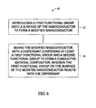
- Figure 6 is a flowchart 10 illustrating this process.
- the conductors are prepared by first introducing 12 a functional group onto a surface of the nanoconductor to form a modified nanoconductor.
- the modified nanoconductor is then mixed 14 with a dispersant, preferably at elevated temperatures, to form a conductive material composition.
- the dispersant is at least bifunctional, and comprises at least a first functional group and a second functional group.
- the functional group on the surface of the modified nanoconductor reacts with the dispersant, and in particular, with one of the functional groups on the dispersant.
- the resulting mixture is a conductive material composition, which may be a resin, paste or ink.
- the conductive material composition may then be applied to the polymeric substrate.
- the remaining unreacted functional group on the dispersant chemically reacts with the polymeric substrate to form a covalent bond. This chemical bonding effectively integrates the conductors and the polymeric substrate, ensuring good stability.
- the present disclosure is directed to a conductive material composition.
- the conductive material composition may be applied to the polymeric substrate to form an integrated product.
- the conductive material composition comprises a conductor, a dispersant, and a solvent.
- the conductors generally include one or more different material types such transparent conductive oxides, metals, and combinations thereof.
- the transparent conductive oxides (TCOs) may include, for example, indium tin oxide (ITO), doped zinc oxide (ZnO), cadmium oxide (CdO), antimony doped tin oxide (Sb-SnO 2 ), and combinations thereof.
- the metal conductors include silver, copper, nickel, gold, and combinations thereof.
- the conductivity of the TCOs is typically on the order of about 10 -4 ohms-centimeter.
- Silver, copper, and gold are typically the best metal conductors and can conduct in the range of about 100 - 1000 times better than the TCOs.
- a hybrid i.e., a combination of two or more
- the conductive materials introduced above may offer improved properties in conductivity and transparency as compared to a conductor that incorporates only a single one of the above listed conductive materials.
- All of the conductive materials can be used at nanometer scales.
- Conductors having such dimensions are generally referred to herein as nanoconductors and include, but are not limited to, nanowires, nanotubes, nanorods, nanobelts, nanoribbons, and nanoparticles. As used herein, the term “conductors” is thus intended to include nanoconductors.
- the conductors are modified to introduce a functional group onto a surface of the conductor.
- Any suitable method may be used to introduce the functional group onto the surface of the conductor. The method used to introduce the functional group may vary depending on the type of conductor.
- the conductor may be a transparent conductive oxide (TCO) and the functional group may be a hydroxyl group.
- TCO transparent conductive oxide
- the hydroxyl group may be introduced onto the surface of the TCO conductor by subjecting the surface of the conductor to a cleaning process, such as is illustrated in Figure 1 .
- a nanowire conductor 100 comprising a conductor material such as indium tin oxide (ITO), is cleaned by sequential ultrasonic cleaning in deionized water, methanol, isopropyl alcohol, and acetone.
- each step of the sequential ultrasonic cleaning is performed for about ten minutes.
- the conductor is dried in air, and then exposed to oxygen plasma 102 for about five minutes at room temperature.
- the oxygen plasma exposure is conducted at an oxygen pressure of about 200 mtorr and a plasma power of about 30W.
- the conductors 100 are then immersed in a 0.05M sodium hydroxide (NaOH) solution for about five minutes and washed thoroughly with copious amounts of deionized water and dried in air.
- aOH sodium hydroxide
- the surface 104 of the ITO nanowire 100 should contain hydroxyl groups 106.
- the conductor 100 may be a transparent conductive oxide and the functional group is an acrylate 154.
- the acrylate functional group 154 can be introduced onto the surface 104 of the conductor by exposing the conductor 100 to an acrylate reagent 144 at a temperature of about 80°C overnight.
- Other functional groups may also be introduced onto the surface of the conductor using similar techniques.
- the modified surface may optionally be further modified by converting the functional group to one or more different functional groups.
- additional functional groups include, but are not limited to, an acrylate, an epoxy group, an ester, an amine, a mercapto group, sulfonyl chloride, vinyl, and a carboxyl group. Any suitable method may be used to convert the first functional group into one or more additional functional groups. This may be done, for example, by reacting the first functional group on the surface of the conductor with one or more reactant.
- the conductor 100 comprising the hydroxyl groups 106 on the surface 104 thereof may be combined with a reactant such as phthalamide 120 or aziridine 122, or other amides or polyimides (not shown).
- a reactant such as phthalamide 120 or aziridine 122, or other amides or polyimides (not shown).
- the resulting reaction converts the hydroxyl groups 106 on the surface 104 of the conductor 100 into amine (NH 2 ) groups 130.
- the hydroxyl groups 106 on the surface 104 of the conductor 100 can be reacted with a reactant such as an ester 140, or an amide, polycarbonate, or polyimide (not shown), at slightly elevated temperatures, which converts the hydroxyl groups 106 into carboxyl groups 150.
- a reactant such as an ester 140, or an amide, polycarbonate, or polyimide (not shown)
- the hydroxyl groups 106 on the surface 104 of the conductor 100 can be reacted with a reactant such as an epoxide 142 at slightly elevated temperatures, which converts the hydroxyl groups 106 into acrylate groups 152.
- Other suitable reactants may also be used.
- the conductor may be a carbon conductor, such as graphene.
- Functional groups may be introduced onto such a conductor by oxidizing graphite using potassium permanganate (KMnO 4 ) and sulfuric acid (H 2 SO 4 ). This oxidation followed by a cleaning process generates hydroxyl groups, epoxide, and carboxyl functional groups on the surface of the graphene. This is illustrated in Figure 2 .
- the modified surface may optionally be further modified by converting the functional group to one or more different functional groups.
- additional functional groups include, but are not limited to, an acrylate, an epoxy group, an ester, an amine, a mercapto group, sulfonyl chloride, vinyl, and a carboxyl group. Any suitable method may be used to convert the first functional group into one or more additional functional groups. This may be done, for example, by reacting the first functional group on the surface of the conductor with one or more reactant, as described above for TCO conductors.
- the modified conductor is mixed with a dispersant, and a solvent, to form a conductive material composition.
- the conductive material composition will comprise the conductor in an amount of from about 0.5% (by weight of the composition) to about 90% (by weight of the composition), and dispersants in an amount of from about 10% (by weight of the composition) to about 90% (by weight of the composition).
- the exact amounts of conductor and dispersant present in the conductive material composition will vary depending on the specific application or requirements of conductivity and transmittance of the product produced.
- the dispersants used in the compositions and methods of the present disclosure help with dispersing the conductors throughout the conductive material composition. Additionally, as noted above, the dispersants also act as a linker to chemically bond the conductors to the polymeric substrate, so that the conductors and polymeric substrate are fully integrated. This chemical bonding is achieved through functional groups present on the dispersant. Specifically, the dispersants are at least bifunctional, comprising at least a first functional group and a second functional group. When the dispersants are mixed with the modified conductors, e.g., at slightly elevated temperatures overnight, the functional group(s) on the surface of the conductor reacts with the dispersant, and in particular, with one of the functional groups on the dispersant.
- This reaction produces a stable, well dispersed conductive material composition, which may be a resin, paste or ink. Additional oligomerization on the modified conductors will improve the dispersity of the conductors in the dispersant.
- the conductive material composition may then be applied to a substrate, e.g., polycarbonates, polyacrylate, polyurethanes, polyimide (PI), polybenzimidazole (PBI), polybenzothiazole (PBT), polybenzoxazole (PBX), polysulfone, epoxy, or related systems.
- the remaining unreacted functional group on the dispersant chemically reacts with the polymeric substrate to form a covalent bond upon application of the composition to the substrate. This chemical bonding effectively integrates the conductors and the polymeric substrate, ensuring good stability.
- functional groups on the conductor may also bond directly onto the polymeric substrate, if the functional groups and polymeric substrate are compatible.
- the dispersant may be any suitable substituted or unsubstitued aliphatic or aromatic compound that is at least bifunctional, i.e., comprises at least a first functional group and a second functional group.
- the first and second functional groups on the dispersant may be the same or alternately may be different functional groups. If the first and second functional groups on the dispersant are the same, preferably, one of the groups is protected during reaction with the conductor. This protection may then be removed prior to application of the conductive material composition to the polymer substrate.
- the dispersant has the structure: R 2 -R 1 -R 3
- R 1 is a substituted or unsubstitued aliphatic or aromatic hydrocarbyl moiety
- R 2 and R 3 are functional groups independently selected from the group consisting of acetyl chloride, carboxyl, ester, isocyanates, vinyl, acrylate, amine, aldehyde, and hydroxyl.
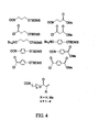
- suitable dispersants are illustrated in Figures 3 and 4 . It should be understood that the specific examples of dispersants illustrated herein are intended to be non-limiting, and thus may be modified without departing from the scope of the current disclosure.
- the conductive material composition may further comprise a solvent.
- the conductive material composition will comprise the solvent in an amount of from about 0.1 % (by weight of the composition) to about 95% (by weight of the composition).
- the specific amount of solvent used depends on the form of the composition (e.g., ink, paste, resin).
- a variety of solvents can be used including methanol, ethanol, isopropyl alcohol, N-dimethylformamide, 2-isopropoxyethanol, tetrahydrofuran, acetonitrile, acetone, ethyleneglycol, 2-methoxyethanol, toluene, xylene, benzene, triethylamine, and combinations thereof.
- the solvents are typically combined with the conductors and dispersants prior to reacting the conductor and dispersant at slightly elevated temperatures, to form the conductive material composition.
- the conductive material composition can be made in the form of resins, pastes, and inks.
- the compositions can be applied on the polymeric substrates by any suitable method such as spin coating, spraying, dip-coating, screen printing, and ink-jet printing.
- the conductive materials composition includes conductors, dispersants, and solvents.
- the conductive materials composition generally includes transparent conductive oxide conductors, including, but not limited to, one or more of indium tin oxide (ITO), doped zinc oxide (ZnO), cadmium oxide (CdO), antimony doped tin oxide (Sb-SnO2);; and metal conductors such as silver, copper, nickel, and gold.
- the conductors can be nanoconductors, and can be nanotubes, nanowires, nanorods, nanobelts, nanoribbons, nanoparticles, or other forms that have a nanoscale dimension.
- the described materials and processes utilize the transparent conductors in nanoscale dimension. As a result, internal stresses are not developed and cracks generally are not initiated within the conductor compositions.
- the process modifies the surface of nano-conductors (e.g., transparent conductors) and incorporates the conductors into a polymer matrix by covalent bonding. By using such a process, the conductors are fully integrated into a matrix structure. Through various combinations of the processes and methods described herein, the resulting conducting layer is rendered a very durable and robust system.
Landscapes
- Chemical & Material Sciences (AREA)
- Physics & Mathematics (AREA)
- Dispersion Chemistry (AREA)
- Spectroscopy & Molecular Physics (AREA)
- Engineering & Computer Science (AREA)
- Nanotechnology (AREA)
- Crystallography & Structural Chemistry (AREA)
- Organic Chemistry (AREA)
- Materials Engineering (AREA)
- General Physics & Mathematics (AREA)
- Condensed Matter Physics & Semiconductors (AREA)
- Composite Materials (AREA)
- Inorganic Chemistry (AREA)
- Manufacturing & Machinery (AREA)
- Manufacturing Of Electric Cables (AREA)
- Non-Insulated Conductors (AREA)
- Conductive Materials (AREA)
- Paints Or Removers (AREA)
- Inks, Pencil-Leads, Or Crayons (AREA)
- Coating Of Shaped Articles Made Of Macromolecular Substances (AREA)
- Laminated Bodies (AREA)
Claims (9)
- Composition de matières conductrices comprenant :une composition formée par le mélange d'un nanoconducteur modifié sélectionné à partir du groupe constitué d'oxydes conducteurs transparents, de métaux, de graphène et de combinaisons de ceux-ci, dans laquelle la surface du nanoconducteur comprend un premier groupe fonctionnel, avec un dispersant comprenant au moins un premier groupe fonctionnel et un second groupe fonctionnel dans lesquels pendant le mélange le premier groupe fonctionnel sur la surface du nanoconducteur modifié réagit avec le dispersant ; et dans laquelleun solvant est sélectionné à partir d'un groupe constitué d'alcool isopropylique, 2-isopropoxyéthanol, tétrahydrofuranne, acétonitrile, 2-méthoxyéthanol, triéthylamine et des combinaisons de ceux-ci ; etle dispersant a une structure de : R2-R1-R3 ;dans laquelle R1 est une fraction hydrocarbyle aliphatique ou aromatique substituée ou non substituée ; et R2 et R3 sont des groupes fonctionnels indépendamment sélectionnés à partir du groupe constitué du chlorure d'acétyle, carboxyle, ester, isocyanates, vinyle, acrylate, amine, aldéhyde et hydroxyle ; et dans laquellela composition est pour application à un substrat polymère.
- Composition de matières conductrices selon la revendication 1, dans laquelle l'oxyde conducteur transparent est sélectionné à partir du groupe constitué d'oxyde d'étain dopé à l'indium, oxyde de zinc dopé, oxyde de cadmium, oxyde d'étain dopé à l'antimoine et des combinaisons de ceux-ci.
- Composition de matières conductrices selon la revendication 1, dans laquelle le métal est sélectionné à partir du groupe constitué par l'argent, le cuivre, le nickel, l'or et des combinaisons de ceux-ci.
- Composition de matières conductrices selon la revendication 1, dans laquelle la composition comprend le nanoconducteur (100) en une quantité d'environ 0,5 % (composition en poids) à environ 90 % (composition en poids).
- Composition de matières conductrices selon la revendication 1, dans laquelle la composition comprend le solvant en une quantité d'environ 0,1 % (composition en poids) à environ 95 % (composition en poids).
- Composition de matières conductrices selon la revendication 1, dans laquelle la composition comprend le dispersant en une quantité d'environ 10 % (composition en poids) à environ 90 % (composition en poids).
- Composition de matières conductrices selon la revendication 1, dans laquelle la composition est une résine, une pâte, ou une encre.
- Procédé de préparation d'un nanoconducteur transparent (100) pour application à un substrat polymère, le procédé comprenant :l'introduction (12) d'un premier groupe fonctionnel sur une surface (104) du nanoconducteur pour former un nanoconducteur modifié, dans lequel le nanoconducteur est sélectionné à partir du groupe constitué d'oxydes conducteurs transparents, de métaux, de graphène et de combinaisons de ceux-ci et le premier groupe fonctionnel sur la surface (104) du nanoconducteur modifié (100) est un groupe hydroxyle (106) ;transformation du groupe d'hydroxyle (106) sur la surface (104) du nanoconducteur modifié (100) en un second groupe fonctionnel sélectionné à partir du groupe constitué d'un acrylate, un groupe époxy, un ester, une amine, un mercapto, chlorure de sulfonyle, vinyle et un groupe carboxyle, etle mélange (14) du nanoconducteur modifié avec un solvant et un dispersant comprenant au moins un premier groupe fonctionnel et un second groupe fonctionnel pour former une composition de matière conductrice, dans laquelle le premier groupe fonctionnel sur la surface du nanoconducteur modifié réagit avec le dispersant ; dans lequelun solvant est sélectionné à partir d'un groupe constitué par de l'alcool isopropylique, 2-isopropoxyéthanol, tétrahydrofuranne, acétonitrile, 2-méthoxyéthanol, triéthylamine et des combinaisons de ceux-ci, etle dispersant a une structure de : R2-R1-R3;dans laquelle R1 est une fraction hydrocarbyle aliphatique ou aromatique substituée ou non substituée ; et R2 et R3 sont des groupes fonctionnels indépendamment sélectionnés à partir du groupe consistant en chlorure d'acétyle, carboxyle, ester, isocyanates, vinyle, acrylate, amine, aldéhyde et hydroxyle ; etcomprenant en outre l'application de la composition de matière conductrice au substrat polymère.
- Procédé selon la revendication 8, dans lequel la composition de matière conductrice est appliquée au substrat polymère par revêtement à la tournette, pulvérisation, revêtement par immersion, impression en sérigraphie, ou impression à jet d'encre.
Applications Claiming Priority (1)
| Application Number | Priority Date | Filing Date | Title |
|---|---|---|---|
| US12/190,025 US8163205B2 (en) | 2008-08-12 | 2008-08-12 | Durable transparent conductors on polymeric substrates |
Publications (3)
| Publication Number | Publication Date |
|---|---|
| EP2154689A2 EP2154689A2 (fr) | 2010-02-17 |
| EP2154689A3 EP2154689A3 (fr) | 2011-09-14 |
| EP2154689B1 true EP2154689B1 (fr) | 2015-07-08 |
Family
ID=41351617
Family Applications (1)
| Application Number | Title | Priority Date | Filing Date |
|---|---|---|---|
| EP09167661.9A Active EP2154689B1 (fr) | 2008-08-12 | 2009-08-11 | Conducteurs transparents longue durée sur substrats polymères |
Country Status (5)
| Country | Link |
|---|---|
| US (1) | US8163205B2 (fr) |
| EP (1) | EP2154689B1 (fr) |
| JP (2) | JP5835864B2 (fr) |
| KR (1) | KR101605899B1 (fr) |
| CN (1) | CN101650981B (fr) |
Families Citing this family (23)
| Publication number | Priority date | Publication date | Assignee | Title |
|---|---|---|---|---|
| JP5380161B2 (ja) * | 2009-06-02 | 2014-01-08 | 株式会社日立製作所 | 透明導電性膜およびそれを用いた電子デバイス |
| US9540498B1 (en) * | 2010-04-03 | 2017-01-10 | Dan Scheffer | Method of coating a substrate with a graphene containing composition |
| US9012294B2 (en) | 2010-07-27 | 2015-04-21 | Panasonic Intellectual Property Management Co., Ltd. | Manufacturing method of non-volatile memory device |
| CN102153065B (zh) * | 2010-11-09 | 2012-05-30 | 厦门大学 | 一种金纳米棒-石墨烯复合膜及其制备方法 |
| CN101962183B (zh) * | 2010-11-09 | 2012-07-04 | 厦门大学 | 一种两亲性石墨烯复合膜及其制备方法 |
| EP2637862B1 (fr) * | 2010-11-10 | 2017-07-26 | National University of Singapore | Conducteur transparent au graphène à couche dipolaire permanente |
| KR20140092809A (ko) * | 2011-09-09 | 2014-07-24 | 보드 오브 트러스티즈 오브 노선 일리노이스 유니버시티 | 결정성 그래핀 및 결정성 그래핀 제조 방법 |
| JP5419955B2 (ja) * | 2011-12-12 | 2014-02-19 | 株式会社東芝 | 透明導電材料、分散液、透明導電膜、及びそれらの製造方法 |
| CN103194116A (zh) * | 2012-01-09 | 2013-07-10 | 深圳市纳宇材料技术有限公司 | 一种油墨、透明导电线路及透明导电线路的制备方法 |
| US20140151606A1 (en) * | 2012-11-30 | 2014-06-05 | Nthdegree Technologies Worldwide Inc. | Ultraviolet-Curable Conductive Ink and Dielectric Ink Compositions Having a Common Binding Medium, with Manufactures and Fabrication Methods |
| CN103059629B (zh) * | 2012-12-28 | 2015-09-30 | 中国科学院过程工程研究所 | 一种氧化锌纳米线导电涂料及其制备方法 |
| CN103194135B (zh) * | 2013-05-02 | 2015-01-21 | 段宝荣 | 一种耐光性涂料的制备方法 |
| CN103436099B (zh) * | 2013-09-11 | 2016-03-09 | 中国科学院宁波材料技术与工程研究所 | 一种复合导电油墨 |
| US9386694B1 (en) | 2014-12-15 | 2016-07-05 | The Boeing Company | Super light weight electronic circuit and low power distribution in aircraft systems |
| CN104479456B (zh) * | 2014-12-23 | 2016-06-01 | 中国科学院化学研究所 | 一种金包银-石墨烯基水性墨水及其喷墨打印透明的图案化导电电极的应用 |
| CN104530829B (zh) * | 2015-01-13 | 2017-08-29 | 中国科学院化学研究所 | 一种氧化石墨烯与金纳米棒复合型墨水及其制备方法 |
| US11047745B2 (en) * | 2015-12-11 | 2021-06-29 | The Boeing Company | Lightweight fire detection systems and methods |
| CN106128556A (zh) * | 2016-06-30 | 2016-11-16 | 嘉兴市高正高分子材料有限公司 | 一种高分散型油系碳纳米管导电浆料的制备方法 |
| CN110049943A (zh) * | 2016-09-27 | 2019-07-23 | 俄亥俄州立大学 | 超导金属复合材料的形式及其合成 |
| CN106832363A (zh) * | 2016-12-31 | 2017-06-13 | 南京新月材料科技有限公司 | 石墨烯改性聚酰亚胺基复合薄膜的制备方法及柔性电路板 |
| US10371982B2 (en) * | 2017-06-23 | 2019-08-06 | Himax Display, Inc. | Display panel |
| FI128435B (en) | 2018-05-09 | 2020-05-15 | Canatu Oy | Electrically conductive multilayer film |
| CN108863312A (zh) * | 2018-07-12 | 2018-11-23 | 李磊 | 一种抗静电陶瓷用高性能抗静电剂及其制备方法 |
Family Cites Families (32)
| Publication number | Priority date | Publication date | Assignee | Title |
|---|---|---|---|---|
| GB1336559A (en) * | 1970-05-20 | 1973-11-07 | Triplex Safety Glass Co | Metal oxide coatings |
| US4248687A (en) * | 1979-07-23 | 1981-02-03 | Massachusetts Institute Of Technology | Method of forming transparent heat mirrors on polymeric substrates |
| DE3136794C2 (de) * | 1981-09-16 | 1983-07-28 | Siemens AG, 1000 Berlin und 8000 München | Lötfähiges Schichtensystem, seine Verwendung und Verfahren zu seiner Herstellung |
| JPH0788424B2 (ja) * | 1987-07-24 | 1995-09-27 | 株式会社小松製作所 | フィルム状導電性高分子の製造方法 |
| US5378404A (en) * | 1991-04-22 | 1995-01-03 | Alliedsignal Inc. | Process for forming dispersions or solutions of electrically conductive conjugated polymers in a polymeric or liquid phase |
| US5626795A (en) * | 1991-11-27 | 1997-05-06 | Uniax Corporation | Optical quality transparent conductors |
| US5424055A (en) * | 1992-03-23 | 1995-06-13 | Mitsui Mining & Smelting Co., Ltd. | Ultraviolet screening composited oxide and process for producing the same |
| US6344271B1 (en) * | 1998-11-06 | 2002-02-05 | Nanoenergy Corporation | Materials and products using nanostructured non-stoichiometric substances |
| DE59913605D1 (de) * | 1998-09-06 | 2006-08-03 | Leibniz Inst Neue Materialien | Verfahren zur herstellung von suspensionen und pulvern auf basis von indium-zinn-oxid und deren verwendung |
| JP2001081357A (ja) * | 1999-09-17 | 2001-03-27 | Nippon Parkerizing Co Ltd | 酸化チタンコーティング液および酸化チタンコーティング膜の形成方法 |
| GB0016844D0 (en) * | 2000-07-10 | 2000-08-30 | Council Cent Lab Res Councils | Nanoparticles |
| US20040265550A1 (en) * | 2002-12-06 | 2004-12-30 | Glatkowski Paul J. | Optically transparent nanostructured electrical conductors |
| US7153620B2 (en) * | 2003-09-23 | 2006-12-26 | Eastman Kodak Company | Transparent invisible conductive grid |
| JP2005096024A (ja) * | 2003-09-24 | 2005-04-14 | Fuji Xerox Co Ltd | ワイヤとその製造方法および該ワイヤを用いた電磁石 |
| US7067328B2 (en) * | 2003-09-25 | 2006-06-27 | Nanosys, Inc. | Methods, devices and compositions for depositing and orienting nanostructures |
| JP2007514632A (ja) * | 2003-11-21 | 2007-06-07 | ナショナル ユニバーシティ オブ アイルランド、 ゴールウエイ | 可溶性金属酸化物および金属酸化物溶液 |
| JP2005171029A (ja) * | 2003-12-09 | 2005-06-30 | Nippon Parkerizing Co Ltd | 塗料組成物、光触媒機能を有する膜の形成方法、及び光触媒部材 |
| JP2005305392A (ja) * | 2004-04-26 | 2005-11-04 | Jsr Corp | アンチモン含有酸化スズ粒子分散液の製造方法及び透明性導電膜 |
| JP4904575B2 (ja) * | 2004-07-23 | 2012-03-28 | 三菱マテリアル株式会社 | 表面改質透明導電性酸化スズ微粉末とその製造方法およびその分散体 |
| US7560161B2 (en) * | 2004-08-09 | 2009-07-14 | Xerox Corporation | Inorganic material surface grafted with charge transport moiety |
| JP4466289B2 (ja) * | 2004-09-01 | 2010-05-26 | 住友金属鉱山株式会社 | 透明導電性微粒子分散液及び透明導電膜形成用塗布液 |
| JP4247182B2 (ja) * | 2004-11-30 | 2009-04-02 | Tdk株式会社 | 透明導電体 |
| ATE532217T1 (de) * | 2005-08-12 | 2011-11-15 | Cambrios Technologies Corp | Verfahren zur herstellung von transparente leiter auf nanodrahtbasis |
| EP1950239B1 (fr) * | 2005-10-28 | 2017-01-04 | Sumitomo Osaka Cement Co., Ltd. | Dispersion transparente d oxyde inorganique, composition de resine contenant des particules d oxyde inorganique, composition pour encapsuler un element luminescent, element luminescent, revetement dur, film fonctionnel optique, piece optique et procede de production d une composition de resine contenant des particules d'oxide inorganique |
| US7608342B2 (en) * | 2005-11-23 | 2009-10-27 | Brewer Science Inc. | Photocurable, conductive, transparent polymer coatings |
| US8859048B2 (en) * | 2006-01-03 | 2014-10-14 | International Business Machines Corporation | Selective placement of carbon nanotubes through functionalization |
| JP2007200775A (ja) * | 2006-01-27 | 2007-08-09 | Bando Chem Ind Ltd | 金属微粒子分散体および金属微粒子分散体を利用した導電材料 |
| JP4848502B2 (ja) * | 2006-02-16 | 2011-12-28 | 国立大学法人 香川大学 | 配線およびその製造方法ならびにそれらを用いた電子部品と電子機器 |
| JP2007297255A (ja) * | 2006-05-03 | 2007-11-15 | The Inctec Inc | カーボンナノチューブを含有する分散液 |
| KR100791260B1 (ko) | 2006-06-29 | 2008-01-04 | 한국과학기술원 | 탄소나노튜브 필름을 이용한 투명전극의 제조방법 |
| JP5247016B2 (ja) * | 2006-08-31 | 2013-07-24 | キヤノン株式会社 | 複合材料及び分散剤の製造方法 |
| JP5035883B2 (ja) * | 2007-02-23 | 2012-09-26 | 独立行政法人産業技術総合研究所 | 金属ナノ粒子パターニング方法および金属ナノ粒子細線 |
-
2008
- 2008-08-12 US US12/190,025 patent/US8163205B2/en active Active
-
2009
- 2009-06-16 CN CN200910142447.1A patent/CN101650981B/zh active Active
- 2009-07-08 KR KR1020090062178A patent/KR101605899B1/ko active Active
- 2009-08-11 EP EP09167661.9A patent/EP2154689B1/fr active Active
- 2009-08-11 JP JP2009186605A patent/JP5835864B2/ja active Active
-
2015
- 2015-02-23 JP JP2015032932A patent/JP6058715B2/ja active Active
Also Published As
| Publication number | Publication date |
|---|---|
| US20100038601A1 (en) | 2010-02-18 |
| JP5835864B2 (ja) | 2015-12-24 |
| JP6058715B2 (ja) | 2017-01-11 |
| CN101650981A (zh) | 2010-02-17 |
| KR20100020419A (ko) | 2010-02-22 |
| KR101605899B1 (ko) | 2016-03-23 |
| US8163205B2 (en) | 2012-04-24 |
| JP2015187975A (ja) | 2015-10-29 |
| CN101650981B (zh) | 2015-07-15 |
| JP2010050094A (ja) | 2010-03-04 |
| EP2154689A2 (fr) | 2010-02-17 |
| EP2154689A3 (fr) | 2011-09-14 |
Similar Documents
| Publication | Publication Date | Title |
|---|---|---|
| EP2154689B1 (fr) | Conducteurs transparents longue durée sur substrats polymères | |
| US9972742B2 (en) | Method for forming a transparent conductive film with metal nanowires having high linearity | |
| US9960293B2 (en) | Method for manufacturing a transparent conductive electrode using carbon nanotube films | |
| US9236162B2 (en) | Transparent conductive ink and transparent conductive pattern forming method | |
| KR101703845B1 (ko) | 이식 도전체 제조를 위한 향상된 cnt/탑코팅 프로세스 | |
| KR101675627B1 (ko) | 도전성 부재, 그 제조 방법, 터치 패널 및 태양 전지 | |
| JP5472889B2 (ja) | 金属ナノワイヤ、及び金属ナノワイヤを含む透明導電体 | |
| US20080317982A1 (en) | Compliant and nonplanar nanostructure films | |
| KR20170066555A (ko) | 투명 코팅 및 투명 전도성 필름을 위한 특성 향상 충진제 | |
| JPWO2010010838A1 (ja) | 透明電極および透明電極の製造方法 | |
| EP2542628A1 (fr) | Revêtements conducteurs transparents de grande surface comprenant des nanotubes de carbone dopés et des composites à nanofils, et leurs procédés de réalisation | |
| JP2008507080A (ja) | 選択的化学修飾によるカーボンナノチューブ被覆物のパターン化 | |
| CN108884377B (zh) | 光固化性密封剂组合物、物品以及有机系太阳能电池 | |
| CN103996457A (zh) | 银纳米线薄膜及其制备方法、阵列基板、显示装置 | |
| JP5646671B2 (ja) | 導電性部材、その製造方法、タッチパネル、及び太陽電池 | |
| JP5341544B2 (ja) | 透明導電性基板、色素増感型太陽電池用透明導電性基板及び透明導電性基板の製造方法 | |
| US20150083466A1 (en) | Method For The Functionalisation Of Metal Nanowires And The Production Of Electrodes | |
| KR101756368B1 (ko) | 유연한 전도성 복합체 필름의 패턴 형성 방법 | |
| WO2013038891A1 (fr) | Elément électroconducteur, procédé de production d'élément électroconducteur, écran tactile et cellule solaire | |
| JP2017028239A (ja) | 染料感応太陽電池用集電極保護膜及びその形成方法並びにこれを含む染料感応太陽電池 | |
| US12162989B2 (en) | Dispersion liquid, conductive film and production method thereof, electrode, and solar cell | |
| US20130130020A1 (en) | Electrode paste composition, electrode for electronic device using the same, and method of manufacturing the same | |
| JP2011143689A (ja) | 導電性被膜の製造方法 | |
| CN111715888B (zh) | 铜基纳米结构体、其制备方法、透明导电膜及电子装置 |
Legal Events
| Date | Code | Title | Description |
|---|---|---|---|
| PUAI | Public reference made under article 153(3) epc to a published international application that has entered the european phase |
Free format text: ORIGINAL CODE: 0009012 |
|
| 17P | Request for examination filed |
Effective date: 20090813 |
|
| AK | Designated contracting states |
Kind code of ref document: A2 Designated state(s): AT BE BG CH CY CZ DE DK EE ES FI FR GB GR HR HU IE IS IT LI LT LU LV MC MK MT NL NO PL PT RO SE SI SK SM TR |
|
| AX | Request for extension of the european patent |
Extension state: AL BA RS |
|
| PUAL | Search report despatched |
Free format text: ORIGINAL CODE: 0009013 |
|
| AK | Designated contracting states |
Kind code of ref document: A3 Designated state(s): AT BE BG CH CY CZ DE DK EE ES FI FR GB GR HR HU IE IS IT LI LT LU LV MC MK MT NL NO PL PT RO SE SI SK SM TR |
|
| AX | Request for extension of the european patent |
Extension state: AL BA RS |
|
| RIC1 | Information provided on ipc code assigned before grant |
Ipc: H01B 1/20 20060101AFI20110809BHEP Ipc: H01B 1/24 20060101ALI20110809BHEP Ipc: H01B 1/22 20060101ALI20110809BHEP |
|
| RIN1 | Information on inventor provided before grant (corrected) |
Inventor name: BURNS, RICHARD,W. Inventor name: ZHOU, CHAOYIN |
|
| 17Q | First examination report despatched |
Effective date: 20120426 |
|
| GRAP | Despatch of communication of intention to grant a patent |
Free format text: ORIGINAL CODE: EPIDOSNIGR1 |
|
| INTG | Intention to grant announced |
Effective date: 20150216 |
|
| GRAS | Grant fee paid |
Free format text: ORIGINAL CODE: EPIDOSNIGR3 |
|
| GRAA | (expected) grant |
Free format text: ORIGINAL CODE: 0009210 |
|
| AK | Designated contracting states |
Kind code of ref document: B1 Designated state(s): AT BE BG CH CY CZ DE DK EE ES FI FR GB GR HR HU IE IS IT LI LT LU LV MC MK MT NL NO PL PT RO SE SI SK SM TR |
|
| REG | Reference to a national code |
Ref country code: GB Ref legal event code: FG4D |
|
| RIN1 | Information on inventor provided before grant (corrected) |
Inventor name: BURNS, RICHARD,W. Inventor name: ZHOU, CHAOYIN |
|
| REG | Reference to a national code |
Ref country code: AT Ref legal event code: REF Ref document number: 735941 Country of ref document: AT Kind code of ref document: T Effective date: 20150715 Ref country code: CH Ref legal event code: EP |
|
| REG | Reference to a national code |
Ref country code: IE Ref legal event code: FG4D |
|
| REG | Reference to a national code |
Ref country code: DE Ref legal event code: R096 Ref document number: 602009032048 Country of ref document: DE |
|
| REG | Reference to a national code |
Ref country code: AT Ref legal event code: MK05 Ref document number: 735941 Country of ref document: AT Kind code of ref document: T Effective date: 20150708 |
|
| REG | Reference to a national code |
Ref country code: NL Ref legal event code: MP Effective date: 20150708 |
|
| REG | Reference to a national code |
Ref country code: LT Ref legal event code: MG4D |
|
| PG25 | Lapsed in a contracting state [announced via postgrant information from national office to epo] |
Ref country code: LV Free format text: LAPSE BECAUSE OF FAILURE TO SUBMIT A TRANSLATION OF THE DESCRIPTION OR TO PAY THE FEE WITHIN THE PRESCRIBED TIME-LIMIT Effective date: 20150708 Ref country code: FI Free format text: LAPSE BECAUSE OF FAILURE TO SUBMIT A TRANSLATION OF THE DESCRIPTION OR TO PAY THE FEE WITHIN THE PRESCRIBED TIME-LIMIT Effective date: 20150708 Ref country code: NO Free format text: LAPSE BECAUSE OF FAILURE TO SUBMIT A TRANSLATION OF THE DESCRIPTION OR TO PAY THE FEE WITHIN THE PRESCRIBED TIME-LIMIT Effective date: 20151008 Ref country code: GR Free format text: LAPSE BECAUSE OF FAILURE TO SUBMIT A TRANSLATION OF THE DESCRIPTION OR TO PAY THE FEE WITHIN THE PRESCRIBED TIME-LIMIT Effective date: 20151009 Ref country code: LT Free format text: LAPSE BECAUSE OF FAILURE TO SUBMIT A TRANSLATION OF THE DESCRIPTION OR TO PAY THE FEE WITHIN THE PRESCRIBED TIME-LIMIT Effective date: 20150708 |
|
| PG25 | Lapsed in a contracting state [announced via postgrant information from national office to epo] |
Ref country code: HR Free format text: LAPSE BECAUSE OF FAILURE TO SUBMIT A TRANSLATION OF THE DESCRIPTION OR TO PAY THE FEE WITHIN THE PRESCRIBED TIME-LIMIT Effective date: 20150708 Ref country code: PT Free format text: LAPSE BECAUSE OF FAILURE TO SUBMIT A TRANSLATION OF THE DESCRIPTION OR TO PAY THE FEE WITHIN THE PRESCRIBED TIME-LIMIT Effective date: 20151109 Ref country code: AT Free format text: LAPSE BECAUSE OF FAILURE TO SUBMIT A TRANSLATION OF THE DESCRIPTION OR TO PAY THE FEE WITHIN THE PRESCRIBED TIME-LIMIT Effective date: 20150708 Ref country code: IS Free format text: LAPSE BECAUSE OF FAILURE TO SUBMIT A TRANSLATION OF THE DESCRIPTION OR TO PAY THE FEE WITHIN THE PRESCRIBED TIME-LIMIT Effective date: 20151108 Ref country code: PL Free format text: LAPSE BECAUSE OF FAILURE TO SUBMIT A TRANSLATION OF THE DESCRIPTION OR TO PAY THE FEE WITHIN THE PRESCRIBED TIME-LIMIT Effective date: 20150708 Ref country code: ES Free format text: LAPSE BECAUSE OF FAILURE TO SUBMIT A TRANSLATION OF THE DESCRIPTION OR TO PAY THE FEE WITHIN THE PRESCRIBED TIME-LIMIT Effective date: 20150708 Ref country code: SE Free format text: LAPSE BECAUSE OF FAILURE TO SUBMIT A TRANSLATION OF THE DESCRIPTION OR TO PAY THE FEE WITHIN THE PRESCRIBED TIME-LIMIT Effective date: 20150708 |
|
| REG | Reference to a national code |
Ref country code: CH Ref legal event code: PL |
|
| REG | Reference to a national code |
Ref country code: DE Ref legal event code: R097 Ref document number: 602009032048 Country of ref document: DE |
|
| PG25 | Lapsed in a contracting state [announced via postgrant information from national office to epo] |
Ref country code: CZ Free format text: LAPSE BECAUSE OF FAILURE TO SUBMIT A TRANSLATION OF THE DESCRIPTION OR TO PAY THE FEE WITHIN THE PRESCRIBED TIME-LIMIT Effective date: 20150708 Ref country code: IT Free format text: LAPSE BECAUSE OF FAILURE TO SUBMIT A TRANSLATION OF THE DESCRIPTION OR TO PAY THE FEE WITHIN THE PRESCRIBED TIME-LIMIT Effective date: 20150708 Ref country code: MC Free format text: LAPSE BECAUSE OF FAILURE TO SUBMIT A TRANSLATION OF THE DESCRIPTION OR TO PAY THE FEE WITHIN THE PRESCRIBED TIME-LIMIT Effective date: 20150708 Ref country code: DK Free format text: LAPSE BECAUSE OF FAILURE TO SUBMIT A TRANSLATION OF THE DESCRIPTION OR TO PAY THE FEE WITHIN THE PRESCRIBED TIME-LIMIT Effective date: 20150708 Ref country code: EE Free format text: LAPSE BECAUSE OF FAILURE TO SUBMIT A TRANSLATION OF THE DESCRIPTION OR TO PAY THE FEE WITHIN THE PRESCRIBED TIME-LIMIT Effective date: 20150708 Ref country code: CH Free format text: LAPSE BECAUSE OF NON-PAYMENT OF DUE FEES Effective date: 20150831 Ref country code: SK Free format text: LAPSE BECAUSE OF FAILURE TO SUBMIT A TRANSLATION OF THE DESCRIPTION OR TO PAY THE FEE WITHIN THE PRESCRIBED TIME-LIMIT Effective date: 20150708 Ref country code: LI Free format text: LAPSE BECAUSE OF NON-PAYMENT OF DUE FEES Effective date: 20150831 |
|
| PLBE | No opposition filed within time limit |
Free format text: ORIGINAL CODE: 0009261 |
|
| STAA | Information on the status of an ep patent application or granted ep patent |
Free format text: STATUS: NO OPPOSITION FILED WITHIN TIME LIMIT |
|
| PG25 | Lapsed in a contracting state [announced via postgrant information from national office to epo] |
Ref country code: RO Free format text: LAPSE BECAUSE OF FAILURE TO SUBMIT A TRANSLATION OF THE DESCRIPTION OR TO PAY THE FEE WITHIN THE PRESCRIBED TIME-LIMIT Effective date: 20150708 |
|
| REG | Reference to a national code |
Ref country code: IE Ref legal event code: MM4A |
|
| 26N | No opposition filed |
Effective date: 20160411 |
|
| PG25 | Lapsed in a contracting state [announced via postgrant information from national office to epo] |
Ref country code: IE Free format text: LAPSE BECAUSE OF NON-PAYMENT OF DUE FEES Effective date: 20150811 |
|
| REG | Reference to a national code |
Ref country code: FR Ref legal event code: PLFP Year of fee payment: 8 |
|
| PG25 | Lapsed in a contracting state [announced via postgrant information from national office to epo] |
Ref country code: SI Free format text: LAPSE BECAUSE OF FAILURE TO SUBMIT A TRANSLATION OF THE DESCRIPTION OR TO PAY THE FEE WITHIN THE PRESCRIBED TIME-LIMIT Effective date: 20150708 |
|
| PG25 | Lapsed in a contracting state [announced via postgrant information from national office to epo] |
Ref country code: MT Free format text: LAPSE BECAUSE OF FAILURE TO SUBMIT A TRANSLATION OF THE DESCRIPTION OR TO PAY THE FEE WITHIN THE PRESCRIBED TIME-LIMIT Effective date: 20150708 |
|
| PG25 | Lapsed in a contracting state [announced via postgrant information from national office to epo] |
Ref country code: HU Free format text: LAPSE BECAUSE OF FAILURE TO SUBMIT A TRANSLATION OF THE DESCRIPTION OR TO PAY THE FEE WITHIN THE PRESCRIBED TIME-LIMIT; INVALID AB INITIO Effective date: 20090811 Ref country code: SM Free format text: LAPSE BECAUSE OF FAILURE TO SUBMIT A TRANSLATION OF THE DESCRIPTION OR TO PAY THE FEE WITHIN THE PRESCRIBED TIME-LIMIT Effective date: 20150708 Ref country code: BG Free format text: LAPSE BECAUSE OF FAILURE TO SUBMIT A TRANSLATION OF THE DESCRIPTION OR TO PAY THE FEE WITHIN THE PRESCRIBED TIME-LIMIT Effective date: 20150708 |
|
| PG25 | Lapsed in a contracting state [announced via postgrant information from national office to epo] |
Ref country code: NL Free format text: LAPSE BECAUSE OF FAILURE TO SUBMIT A TRANSLATION OF THE DESCRIPTION OR TO PAY THE FEE WITHIN THE PRESCRIBED TIME-LIMIT Effective date: 20150708 Ref country code: CY Free format text: LAPSE BECAUSE OF FAILURE TO SUBMIT A TRANSLATION OF THE DESCRIPTION OR TO PAY THE FEE WITHIN THE PRESCRIBED TIME-LIMIT Effective date: 20150708 |
|
| PG25 | Lapsed in a contracting state [announced via postgrant information from national office to epo] |
Ref country code: BE Free format text: LAPSE BECAUSE OF NON-PAYMENT OF DUE FEES Effective date: 20150831 |
|
| REG | Reference to a national code |
Ref country code: FR Ref legal event code: PLFP Year of fee payment: 9 |
|
| PG25 | Lapsed in a contracting state [announced via postgrant information from national office to epo] |
Ref country code: TR Free format text: LAPSE BECAUSE OF FAILURE TO SUBMIT A TRANSLATION OF THE DESCRIPTION OR TO PAY THE FEE WITHIN THE PRESCRIBED TIME-LIMIT Effective date: 20150708 |
|
| PG25 | Lapsed in a contracting state [announced via postgrant information from national office to epo] |
Ref country code: LU Free format text: LAPSE BECAUSE OF NON-PAYMENT OF DUE FEES Effective date: 20150811 |
|
| PG25 | Lapsed in a contracting state [announced via postgrant information from national office to epo] |
Ref country code: MK Free format text: LAPSE BECAUSE OF FAILURE TO SUBMIT A TRANSLATION OF THE DESCRIPTION OR TO PAY THE FEE WITHIN THE PRESCRIBED TIME-LIMIT Effective date: 20150708 |
|
| REG | Reference to a national code |
Ref country code: FR Ref legal event code: PLFP Year of fee payment: 10 |
|
| REG | Reference to a national code |
Ref country code: DE Ref legal event code: R082 Ref document number: 602009032048 Country of ref document: DE Representative=s name: KILBURN & STRODE LLP, NL |
|
| P01 | Opt-out of the competence of the unified patent court (upc) registered |
Effective date: 20230516 |
|
| PGFP | Annual fee paid to national office [announced via postgrant information from national office to epo] |
Ref country code: DE Payment date: 20250827 Year of fee payment: 17 |
|
| PGFP | Annual fee paid to national office [announced via postgrant information from national office to epo] |
Ref country code: GB Payment date: 20250827 Year of fee payment: 17 |
|
| PGFP | Annual fee paid to national office [announced via postgrant information from national office to epo] |
Ref country code: FR Payment date: 20250825 Year of fee payment: 17 |