EP2159843B1 - Dispositif d'affichage à couleur et son procédé de fabrication - Google Patents
Dispositif d'affichage à couleur et son procédé de fabrication Download PDFInfo
- Publication number
- EP2159843B1 EP2159843B1 EP09010980.2A EP09010980A EP2159843B1 EP 2159843 B1 EP2159843 B1 EP 2159843B1 EP 09010980 A EP09010980 A EP 09010980A EP 2159843 B1 EP2159843 B1 EP 2159843B1
- Authority
- EP
- European Patent Office
- Prior art keywords
- sub
- pixel
- light
- reflection layer
- layer
- Prior art date
- Legal status (The legal status is an assumption and is not a legal conclusion. Google has not performed a legal analysis and makes no representation as to the accuracy of the status listed.)
- Active
Links
Images


Classifications
-
- H—ELECTRICITY
- H10—SEMICONDUCTOR DEVICES; ELECTRIC SOLID-STATE DEVICES NOT OTHERWISE PROVIDED FOR
- H10K—ORGANIC ELECTRIC SOLID-STATE DEVICES
- H10K59/00—Integrated devices, or assemblies of multiple devices, comprising at least one organic light-emitting element covered by group H10K50/00
- H10K59/30—Devices specially adapted for multicolour light emission
- H10K59/35—Devices specially adapted for multicolour light emission comprising red-green-blue [RGB] subpixels
- H10K59/351—Devices specially adapted for multicolour light emission comprising red-green-blue [RGB] subpixels comprising more than three subpixels, e.g. red-green-blue-white [RGBW]
-
- H—ELECTRICITY
- H10—SEMICONDUCTOR DEVICES; ELECTRIC SOLID-STATE DEVICES NOT OTHERWISE PROVIDED FOR
- H10K—ORGANIC ELECTRIC SOLID-STATE DEVICES
- H10K50/00—Organic light-emitting devices
- H10K50/80—Constructional details
- H10K50/85—Arrangements for extracting light from the devices
- H10K50/852—Arrangements for extracting light from the devices comprising a resonant cavity structure, e.g. Bragg reflector pair
-
- H—ELECTRICITY
- H10—SEMICONDUCTOR DEVICES; ELECTRIC SOLID-STATE DEVICES NOT OTHERWISE PROVIDED FOR
- H10K—ORGANIC ELECTRIC SOLID-STATE DEVICES
- H10K59/00—Integrated devices, or assemblies of multiple devices, comprising at least one organic light-emitting element covered by group H10K50/00
- H10K59/10—OLED displays
- H10K59/12—Active-matrix OLED [AMOLED] displays
- H10K59/124—Insulating layers formed between TFT elements and OLED elements
-
- H—ELECTRICITY
- H10—SEMICONDUCTOR DEVICES; ELECTRIC SOLID-STATE DEVICES NOT OTHERWISE PROVIDED FOR
- H10K—ORGANIC ELECTRIC SOLID-STATE DEVICES
- H10K59/00—Integrated devices, or assemblies of multiple devices, comprising at least one organic light-emitting element covered by group H10K50/00
- H10K59/80—Constructional details
- H10K59/875—Arrangements for extracting light from the devices
- H10K59/876—Arrangements for extracting light from the devices comprising a resonant cavity structure, e.g. Bragg reflector pair
-
- H—ELECTRICITY
- H10—SEMICONDUCTOR DEVICES; ELECTRIC SOLID-STATE DEVICES NOT OTHERWISE PROVIDED FOR
- H10K—ORGANIC ELECTRIC SOLID-STATE DEVICES
- H10K59/00—Integrated devices, or assemblies of multiple devices, comprising at least one organic light-emitting element covered by group H10K50/00
- H10K59/30—Devices specially adapted for multicolour light emission
- H10K59/38—Devices specially adapted for multicolour light emission comprising colour filters or colour changing media [CCM]
Definitions
- the present invention relates to a color display device using an electroluminescent device and a method for manufacturing the same.
- CRTs cathode ray tubes
- organic electroluminescent device also referred to hereinafter as "organic EL device”
- organic EL device is an element that emits light according to electrical signals and is composed of an organic compound as a light-emitting material.
- the organic EL device inherently has excellent display properties such as wide viewing angle, high contrast and high-speed response.
- the organic EL device is capable of realizing thin, lightweight and high-definition display devices ranging in size from small to large, and thus attracts attention as an element substituted for CRT or LCD.
- an organic EL display device provided with a micro-cavity (minute resonator) is disclosed (see, for example, Japanese National-Phase Publication No. 2007-503093 ).
- one pixel is divided into red (R), green (G) and blue (B) sub-pixels each constituting a resonator for resonating emitted light between an optically semitransparent reflection electrode and a reflection film (electrode) and having an organic EL light-emitting layer in common among the sub-pixels, thus making separate forming in three colors unnecessary and a color filter also unnecessary, thereby being assumed to provide a simple full-color display device.
- a resonant is not arranged in a white sub-pixel region.
- a light-emitting device wherein a resonant structure is formed by changing the thickness of an anode for an organic electroluminescence layer, thereby picking out R, G and B lights, is disclosed (see, for example, Japanese Patent Application Laid-Open ( JP-A) No. 2006-269329 ).
- the anode a transparent electroconductive material such as ITO is used, and a light reflection film is arranged via a transparent insulation film in the lower part of the anode.
- a white sub-pixel is important for simultaneously achieving rich color reproduction, tone reproduction and low power consumption, and it is desired to solve the problems in arrangement of the white sub-pixel.
- WO 2005/101541 , US 2006/290274 , US 2007/286944 and US 2005/040756 disclose color displays with resonant cavities to generate the colors.
- the present invention has been made in view of the above circumstances and provides a color display device and a method for manufacturing the same.
- a first aspect of the invention is defined in independent device claim 1 and a second aspect is defined in method claim 7.
- the display device of the invention includes plural pixels on a substrate, each pixel contains two or more sub-pixels, each sub-pixel emits light of different wavelength in the visible range and further contains a white sub-pixel.
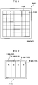
- the display device of the invention has a matrix-type screen panel having plural pixels arranged lengthwise and breadthwise on a substrate.
- Each pixel contains plural sub-pixels, each sub-pixel emits light of different wavelengths in the visible range and further contains a white sub-pixel and each sub-pixel forms a resonator.
- These sub-pixels are independently regulated and allowed to emit lights with independent luminance, thereby enabling full-color reproduction.
- Each pixel is composed of a red (R) sub-pixel, a green (G) sub-pixel, a blue (B) sub-pixel and a white (W) sub-pixel.
- FIG. 2 is a conceptual diagram showing the arrangement of sub-pixels.
- the color display device of the invention includes plural pixels on a substrate, each pixel contains plural sub-pixels, each sub-pixel emits light of different wavelengths in the visible range, and further contains a white sub-pixel, wherein the plural sub-pixels and the white sub-pixel each have a white-light emitting organic electroluminescence layer interposed between an optically semitransparent reflection layer and a light reflection layer, the optical distance between the optically semitransparent reflection layer and the light reflection layer in each of the plural sub-pixels forms a resonator having a distance for resonating emitted light, and the optical distance between the optically semitransparent reflection layer and the light reflection layer in the white sub-pixel is longer than the maximum optical distance between the optically semitransparent reflection layer and the light reflection layer in each of the plural sub-pixels.
- the display device has, as the plural sub-pixels, a red sub-pixel (R sub-pixel), a green sub-pixel (G sub-pixel) and a blue sub-pixel (B sub-pixel), and the optical distances between the optically semitransparent reflection layer and the light reflection layer in the red sub-pixel, green sub-pixel and blue sub-pixel are distances with which red light (R light), green light (G light) and blue light (B light) are resonated respectively.
- R sub-pixel red sub-pixel
- G sub-pixel green sub-pixel
- B sub-pixel blue sub-pixel
- the optical distance between the optically semitransparent reflection layer and the light reflection layer in the white sub-pixel is equal to or longer than twice the maximum optical distance between the optically semitransparent reflection layer and the light reflection layer in each of the plural sub-pixels.
- the optical distance between the optically semitransparent reflection layer and the light reflection layer in the white sub-pixel is 2.0 ⁇ m or more, more preferably 3.0 ⁇ m or more, even more preferably 4.0 ⁇ m or more.
- Each sub-pixel has an optical path length regulation layer between the optically semitransparent reflection layer and the light reflection layer, and the plural sub-pixels and the white sub-pixel each have a white organic electroluminescence layer having the same composition and are different in only the thickness of the optical path length regulation layer.
- the display device of the invention is provided in each sub-pixel region with a TFT for driving each sub-pixel.
- the substrate for the display device of the invention uses, as the substrate, a substrate for a TFT, and at least one of the sub-pixels has a planarized film on the substrate and a light reflection layer on the planarized film. Further, a light path length regulation layer, a white organic luminescence layer and an optically semitransparent reflection layer are arranged on the light reflection layer.
- each sub-pixel has the light reflection layer either between the planarizing film and the substrate or in the planarizing film.
- at least a part of the planarizing film functions as an optical path length regulation layer.
- the red sub-pixel, the green sub-pixel, the blue sub-pixel and the white sub-pixel each have, on the planarizing film, a light reflection layer, an optically semitransparent reflection layer and an optical path length regulation layer and a white light-emitting organic luminescence layer interposed between the optically semitransparent reflection layer and the light reflection layer.
- the red sub-pixel, the green sub-pixel and the blue sub-pixel each have, on the planarizing film, a light reflection layer, an optically semitransparent reflection layer and an optical path length regulation layer and a white organic luminescence layer interposed between the optically semitransparent reflection layer and the light reflection layer
- the white sub-pixel has a light reflection layer between a substrate and a planarizing film and has, on the planarizing film, a transparent electrode, a white organic luminescence layer, and an optically semitransparent reflection layer.
- the light reflection layer of the white sub-pixel is formed at a layer common with an electrode of a TFT.
- a red color filter, a green color filter and a blue color filter are arranged at the light emission side of the red light-emitting sub-pixel, green light-emitting sub-pixel and blue light-emitting sub-pixel, respectively.
- the organic EL in the invention is a top emission-type organic EL.
- FIG. 3 is a sectional schematic diagram showing the constitution of R, G and B sub-pixels and W sub-pixel constituting one pixel in in a comparative non-claimed example.
- a planarizing film 6 is formed by coverage on substrate 1 provided with TFT.
- a light reflection layer 2 is arranged on the planarizing film.
- the light reflection layer may be arranged in common among R, G, B and W sub-pixels.
- optical path length regulation layers that are different in thickness among the R, G, B and W sub-pixels are arranged respectively (that is, optical path length regulation layers 8-1, 8-2, 8-3 and 8-4).
- the optical path length regulation layer 8-1 in the B sub-pixel region is thinnest, and as long as the B sub-pixel region attains a resonance distance, the thickness may be 0, that is, the optical path length regulation layer may not be arranged in the B sub-pixel region.
- the optical path length regulation layer in the R sub-pixel region is thicker than in the G sub-pixel region.
- the optical path length regulation layer 8-4 in the W sub-pixel region is thickest and is preferably thicker than the optical path length regulation layer 8-3 in the R sub-pixel region, more preferably thicker than twice the optical path length regulation layer 8-3 in the R sub-pixel region.
- the optical path length regulation layer is electrically insulating.
- a transparent electrode 3 is arranged as a pixel electrode by patterning on the optical path length regulation layer for each pixel.
- the transparent electrode 3 is connected electrically via a contact hole to TFT.
- the non-light-emitting regions in spaces among the sub-pixels are covered with a bank 7 (insulating layer).
- a white organic luminescence layer 4 and an optically semitransparent reflection layer 5 are arranged thereon in common among the respective sub-pixels.
- the white organic electroluminescence layer 4 is preferably a laminate of plural functional layers such as a hole injecting layer, a hole transporting layer, a light-emitting layer, an electron transporting layer, and an electron injecting layer.
- the optically semitransparent reflection layer 5 may be either a metallic thin film (Al, Ag etc.) or a distributed Bragg reflection film (DBR) wherein transparent thin films different in refractive index are laminated.
- the optical path length regulation layer is composed of an insulating layer material and may be any of inorganic materials (SiO 2 , SiON, SiN etc.) and organic materials (polycarbonate, polyacrylate, silicone resin etc.).
- the thickness of the optical path length regulation in each of the R, G, and B sub-pixels is regulated so as to provide a distance with which emitted light resonates.
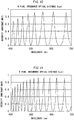
- the resonance optical distance in the B sub-pixel region is 380 nm, emitted light having a maximum wavelength at 465 nm shown in FIG. 6 is picked out to the outside.
- each of R, G and B sub-pixels emits light of different wavelengths in the visible range.
- the optical path length regulation layer is thicker than in the R sub-pixel region and is regulated to have such thickness as not to exhibit emission of light having a specific wavelength in the visible range.
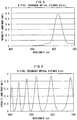
- the resonance optical distance is 2.0 ⁇ m
- lights with a resonance wave having many emission peaks as shown in FIG. 9 are picked out to the outside. Accordingly, the light of W sub-pixel observed outside is an almost white light having such lights mixed therein.
- the lights emitted in the white organic electroluminescence layer 4 upon electrification are repeatedly reflected and resonated between the optically semitransparent reflection layer 5 and the light reflection layer 2 whereby R, G and B lights are emitted through the optically semitransparent reflection layer 5 to the outside.
- the R, G and B resonated lights are mixed and observed as white light.
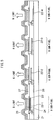
- FIG. 4 is a sectional schematic diagram showing the constitution of one pixel in the invention.
- the constitution of the R, G and B sub-pixel regions is the same as the constitution shown in FIG. 3 .
- a reflection layer 12-2 is first arranged in a region where the W sub-pixel is to be arranged on substrate 11 provided with TFT. TFT and the light reflection layer 12-2 are covered by arranging a planarizing film 16 thereon.
- the planarizing film is arranged as planarizing film 16 common among the R, G and B sub-pixel regions.
- the planarizing film 16 functions as an optical path length regulation layer, wherein the thickness of the optical path length regulation layer in the W sub-pixel may be greater than a predetermined thickness and may thus not be strictly regulated. Accordingly, sufficiently satisfactory performance can be achieved even by a general manner of producing a planarizing film.
- 12-1 represents a light reflection layer
- 18-1, 18-2 and 18-3 each represents an optical path length regulation layer.
- a transparent electrode 13 is arranged as a pixel electrode on the planarizing film 16 by patterning for each sub-pixel.
- the transparent electrode 13 is connected electrically via a contact hole to the TFT.
- the non-light-emitting regions in spaces among the sub-pixels are covered with a bank 17 (insulating layer).
- a white organic luminescence layer 14 and an optically semitransparent reflection layer 15 are arranged thereon in common among the sub-pixels.
- an optical path length regulation layer may be arranged between the planarizing film 16 and the transparent electrode 13.
- FIG. 5 is a sectional schematic diagram showing the constitution of one pixel in still another comparative example.
- the constitution of the W sub-pixel region is the same as the constitution shown in FIG. 4 .
- the light reflection layer is arranged inside the planarizing film.
- the light reflection layer 22-1 is arranged in the uppermost part of the planarizing film 26.
- the light reflection layers 22-2 and 22-3 in the G and R sub-pixel regions are arranged respectively inside the planarizing film 26 in such positions that the resonance distance in the R sub-pixel region becomes longer than that in the G sub-pixel region.
- a patterned transparent electrode 23 is formed in the R, G, B and W sub-pixels, respectively.
- a white organic luminescence layer 24 and a optically semitransparent reflection layer 25 are arranged thereon in common among the R, G, B and W sub-pixels.
- 27 represents a bank.
- the light emitted from each of the R, G and B sub-pixels is a light of high luminance and high chroma with a narrow spectrum distribution, whereby a light with extremely high luminance and high chroma is obtained.
- the light emitted from the W pixel region is not a resonance light having a limited number of specific wavelengths but a white light obtained by mixing of a large number of resonance lights so that a high-luminance white light can be obtained without such color drift as is observed in the conventional W pixel region having a resonator.
- the white organic luminescence layer and semitransparent reflection layer can be formed consistently in common among the R, G, B and W sub-pixels, thus making achievement of higher resolution easy, facilitating the production process, and attaining high productivity.
- the optical path length regulation layer in the invention is not particularly limited as long as it is composed of a transparent insulating layer material, and such material may be any one of inorganic materials (SiO 2 , SiON, SiN etc.) and organic materials (polycarbonate, polyacrylate, silicone resin etc.).
- the inorganic insulating materials used in the optical path length regulation layer of the invention may be a wide variety of conventionally known metal oxides, metal nitrides and metal fluorides.
- metal oxides include MgO, SiO, SiO 2 , Al 2 O 3 , GeO, NiO, CaO, BaO, Fe 2 O 3 , Y 2 O 3 , TiO 2 etc.
- metal nitrides include SiN x , SiN x O y etc.
- metal fluorides include MgF 2 , LiF, AlF 3 , CaF 2 etc. The material may also be a mixture thereof.
- an organic compound may also be used, and a film-forming polymer is preferably used.
- the film-forming polymer includes polycarbonate, polyacrylate, silicone resin, polyvinyl butyral, etc.
- the thickness of the optical path length regulation layer is regulated so as to constitute an optical distance with which each sub-pixel can efficiently resonate light of specific wavelength. Accordingly, the optical distance for resonance is determined depending on the refractive index, composition and thickness of the material interposed between the reflection film and the semitransparent reflection film and is thus not determined by the optical path length regulation layer.
- the thickness of the optical path length regulation layer of each of the R, G and B sub-pixels in terms of physical thickness, is preferably 0 nm to 1000 nm, more preferably 20 nm to 500 nm, even more preferably 30 nm to 200 nm.
- the method of forming the optical path length regulation layer is not particularly limited and can use, for example, a vacuum deposition method, a sputtering method, a reactive sputtering method, an MBE (molecular beam epitaxy) method, a cluster ion beam method, an ion plating method, a plasma polymerization method (high-frequency excitation ion plating method), a plasma CVD method, a laser CVD method, a thermal CVD method, a gas-source CVD method, a coating method, a printing method, or a transfer method.
- a vacuum deposition method a sputtering method, a reactive sputtering method, an MBE (molecular beam epitaxy) method, a cluster ion beam method, an ion plating method, a plasma polymerization method (high-frequency excitation ion plating method), a plasma CVD method, a laser CVD method, a thermal CVD method, a gas-source CVD method,
- the organic luminescence layer in the invention may, besides the light-emitting layer, have conventionally known organic compound layers such as a hole transporting layer, an electron transporting layer, a blocking layer, an electron injecting layer and a hole injecting layer.
- At least one of the pair electrodes of the organic electroluminescence layer of the invention is a transparent electrode, and the other is a back plate.
- the back plate may be transparent or opaque.
- the layer structure of the organic compound layer is not particularly limited, and may be suitably selected in accordance with the usage of the organic electroluminescent device or the target thereof.
- the organic compound layer is formed on the transparent electrode or on the back plate.
- the organic compound layer is formed over the entire surface or on a part of the surface of the transparent electrode or the back plate.
- the shape, the size, the thickness and other factors of the organic compound layer are not particularly limited, and can be suitably selected in accordance with the target.
- the layer structure includes the following. In the invention, however, the layer structure is not limited to these structures.
- the hole transporting layer used in the invention comprises a hole transporting material.
- a hole transporting material a material having any one of a function of transporting holes and a function of blocking electrons injected from the cathode can be used without any special limitation.
- the hole transporting material used in the invention may be any one of a low molecular weight hole transporting material and a high molecular weight hole transporting material.
- hole transporting material used in the invention include the following: A carbazole derivative, an imidazole derivative, a polyarylalkane derivative, a pyrazoline derivative, a pyrazolone derivative, a phenylenediamine derivative, an arylamine derivative, an amino-substituted chalcone derivative, a styrylanthracene derivative, a fluorenone derivative, a hydrazone derivative, a stilbene derivative, a silazane derivative, an aromatic tertiary amine compound, a styrylamine compound, an aromatic dimethylidyne compound, a porphyrin compound, a polysilane compound, a poly(N-vinylcarbazole) derivative, electroconductive polymers or oligomers such as an aniline copolymer, a thiophene oligomer and polythiophene, a polythiophene derivative, a polyphenylene derivative, a polyphenylene derivative,
- the thickness of the hole transporting layer is preferably 1 nm to 200 nm, more preferably 5 nm to 100 nm.
- a hole injecting layer may be formed between the hole transporting layer and the anode.
- the hole injecting layer is a layer which makes it easy to inject holes from the anode to the hole transporting layer.
- a material having a small ionization potential among the above-mentioned various hole transporting materials is preferably used.
- the material include a phthalocyanine compound, a porphyrin compound, and a star-burst triarylamine compound. These can be preferably used.
- the film thickness of the hole injecting layer is preferably 1 nm to 300 nm.
- the light-emitting layer used in the invention comprises at least one light-emitting material, and may comprise a hole transporting material, an electron transporting material, and a host material if necessary.
- the light-emitting material used in the invention is not particularly limited, and may be any one of a fluorescent light-emitting material and a phosphorescent light-emitting material.
- the phosphorescent light-emitting material is preferable from the viewpoint of light-emitting efficiency.
- One kind of light-emitting material may be used if white light can be emitted, or plural light-emitting materials may be simultaneously used.
- plural light-emitting materials are simultaneously used, the combination of emission colors is not particularly limited, and examples include combined use of a blue light-emitting material and a yellow light-emitting material and combined use of a blue light-emitting material, a green light-emitting material and a red light-emitting material.
- the fluorescent light-emitting material examples include a benzooxazole derivative, a benzoimidazole derivative, a benzothiazole derivative, a styrylbenzene derivative, a polyphenyl derivative, a diphenylbutadiene derivative, a tetraphenylbutadiene derivative, a naphthalimide derivative, a coumalin derivative, a perylene derivative, a peronone derivative, an oxadiazole derivative, an aldazine derivative, a pyrrolizine derivative, a cyclopentadiene derivative, a bisstyrylanthracene derivative, a quinacridone derivative, pyrrolopyridine derivative, a thiadiazolopyridine derivative, a styrylamine derivative, an aromatic dimethylidyne compound, various metal complexes, typical example of which include a metal complex of an 8-quinolinol derivative or a rare earth complex, and polymeric compounds
- the phosphorescent light-emitting material is not particularly limited, and is preferably an orthometal metal complex or a porphyrin complex.
- orthometal metal complex is the generic name for the compound group mentioned in " Organic metal chemistry - basic and application -" written by Akio Yamamoto, p. 150, p. 232, Shokabo Publishing Co., Ltd., (published in 1982 ), " Photochemistry and photophysics of coordination compounds” written by H. Yersin, p. 71 to 77, p. 135 to 146, Springer-Verlag (published in 1987 ) and the like. It is advantageous to use the orthometal metal complex in the luminescent layer as the light-emitting material in terms of obtaining a high luminosity and an excellent light-emitting efficiency.
- ligands can be used for forming the above-mentioned orthometal metal complex, and examples thereof are described in the above-mentioned articles.
- preferable examples of the ligands include a 2-phenyl pyridine derivative, a 7,8-benzoquinoline derivative, a 2-(2-thienyl) pyridine derivative, a 2-(1-naphtyl) pyridine derivative, a 2-phenyl quinoline derivative and the like. These derivatives may have a substituent in accordance with necessity.
- the above-mentioned orthometal metal complex may have another ligand in addition to the above-mentioned ligand.
- the orthometal metal complex used in the present invention can be synthesized by various known methods such as those mentioned in: Inorg Chem., vol. 30, p. 1685 (1991 ); Inorg Chem., vol. 27, p. 3464 (1988 ); Inorg Chem., vol. 33, p. 545(1994 ); Inorg. Chim. Acta, vol. 181, p. 245 (1991 ); J. Organomet. Chem., vol. 335, p. 293 (1987 ); J. Am. Chem. Soc. vol. 107, p. 1431 (1985 ); or the like.
- a compound which provide light emission by a triplet exciton can be preferably used in the present invention in terms of improvement of the light-emitting efficiency.
- porphyrin complexes a porphyrin platinum complex is preferable.
- the phosphorescent light-emitting materials may be used alone or in combination of plural kinds thereof.
- One or more kinds of the fluorescent light-emitting materials and one or more kinds of the phosphorescent light-emitting materials may be used together.
- the host material is a material which has a function of moving energy from an excited state thereof to a fluorescent light-emitting material or a phosphorescent light-emitting material, so as to cause the fluorescent or phosphorescent light-emitting material to emit light.
- the host material is not particularly limited if the material is a compound capable of moving the energy of its excitons to the light-emitting material, and can be suitably selected in accordance with the purpose of the electroluminescent device.
- Specific examples thereof include a carbazole derivative, a triazole derivative, an oxazole derivative, an oxadiazole derivative, an imidazole derivative, a polyarylalkane derivative, a pyrazoline derivative, a pyrazolone derivative, a phenylenediamine derivative, an arylamine derivative, an amino-substituted chalcone derivative, a styrylanthracene derivative, a fluorenone derivative, a hydorazone derivative, a stylbene derivative, a silazane derivative, an aromatic tertiary amine compound, a styrylamine compound, an aromatic dimethylidyne compound, a porphyrin compound, an anthraquinodimethane
- the content by percentage of the host material in the light-emitting layer is preferably 20 to 99.9% by mass, more preferably 50 to 99.0% by mass.
- a blocking layer may be formed between the light-emitting layer and the electron transporting layer in the invention.
- the blocking layer is a layer for restraining the diffusion of excitons generated in the light-emitting layer, or restraining holes from penetrating toward the cathode.
- the material used in the blocking layer is not particularly limited if the material is a material capable of receiving electrons from the electron transporting layer and delivering the electrons to the light-emitting layer.
- the material may be an ordinary electron transporting material. Examples thereof include the following: a triazole derivative, an oxazole derivative, an oxadiazole derivative, a fluorenone derivative, an anthraquinodimethane derivative, an anthrone derivative, a diphenylquinone derivative, a thiopyrandioxide derivative, a carbodiimide derivative, a fluorenylidenemethane derivative, a distyrylpyrazine derivative, heterocyclic tetracarboxylic acid anhydrides such as naphthaleneperylene, various metal complexes, typical examples of which include metal complexes of a phthalocyanine derivative or 8-quinolinol derivative, metal phthalocyanine, and metal complexes each having, as a lig
- An electron transporting layer comprising an electron transporting material can be deposited in the invention.
- the electron transporting material is not limited if the material is a material having any one of a function of transporting electrons and a function of blocking holes injected from the anode. Examples of the electron transporting material given in the description of the blocking layer can be preferably used.
- the thickness of the electron transporting layer is preferably 10 nm to 200 nm, more preferably 20 nm to 80 nm.
- the thickness is more than 100 nm, the driving voltage may unfavorably rise. If the thickness is less than 10 nm, the light-emitting efficiency of the electroluminescent device may unfavorably be impaired.
- An electron injecting layer may be formed between the electron transporting layer and the cathode in the invention.
- the electron injecting layer is a layer which makes it easy to inject electrons from the cathode to the electron transporting layer.
- the material used in this layer include alkali metal salts such as lithium fluoride, lithium chloride, lithium bromide, other lithium salts, sodium fluoride, sodium chloride and cesium fluoride, and insulating metal oxides such as lithium oxide, aluminum oxide, indium oxide and magnesium oxide.
- the film thickness of the electron injecting layer is preferably 0.1 nm to 5 nm.
- the material of the substrate used in the invention is preferably a material through which water content cannot permeate, or a material having a very low water content permeability. Also, the material is preferably a material which does not cause scattering or attenuation of light emitted from the organic compound layer.
- organic materials such as YSZ (yttria-stabilized zirconia) and glass
- organic materials such as polyethylene terephthalate, polybutylene terephthalate, polyethylene naphthalate, other polyesters, polystyrene, polycarbonate, polyethersulfone, polyarylate, allyl diglycol carbonate, polyimide, polycycloolefin, norbornene resin, poly(chlorotrifluoroethylene) and other synthetic resins.
- the organic materials it is preferred that the organic materials are organic materials excellent in heat resistance, dimensional stability, solvent resistance, electric non-conductance, workability, low gas permeability and low hygroscopicity.
- the above-mentioned materials may be used alone or in combination of plural kinds thereof.
- the shape, structure and size of the substrate and other factors thereof are not particularly limited, and can be suitably selected in accordance with the usage and purpose of the electroluminescent device.
- the shape is a form of a plate.
- the structure may be a mono-layered structure or a multi-layered structure.
- the substrate may be made of a single member, or plural members.
- the substrate may be transparent and colorless, or transparent and colored.
- the substrate is preferably transparent and colorless since the substrate does not cause scattering or attenuation of light emitted from the light-emitting layer.
- a moisture permeation preventing layer (gas barrier layer) on the front surface or the rear surface (on the side of the transparent electrode) of the substrate.
- the material of this layer is preferably an inorganic material such as silicon nitride or silicon oxide.
- This layer can be formed by, for example, high-frequency sputtering.
- a hard coat layer, an undercoat layer, or some other layer may be formed on the substrate.
- either the first or second electrode may be an anode or a cathode, but it is preferable that the first electrode is an anode and the second electrode is a cathode.
- the anode used in the invention has a function of supplying holes to the organic compound layer.
- the shape, structure and size thereof, and other factors thereof are not particularly limited, and can be suitably selected from known anodes in accordance with the usage and the purpose of the electroluminescent device.
- the material of the anode include metals, alloys, metal oxides, organic electroconductive compounds, and mixtures thereof.
- the material is preferably a material having a work function of 4.0 eV or more.
- Specific examples thereof include semiconductive metal oxides such as a tin oxide doped with antimony or fluorine (ATO, or FTO), tin oxide, zinc oxide, indium oxide, indium tin oxide (ITO) and indium zinc oxide (IZO), metals such as gold, silver, chromium and nickel, mixtures or laminates each made of one or more of these metals and an electroconductive metal oxide, inorganic electroconductive materials such as copper iodide and copper sulfide, organic electroconductive materials such as polyaniline, polythiophene and polypyrrole, and laminates each composed of one or more of these compounds and ITO.
- ATO antimony or fluorine
- ITO indium oxide
- IZO indium zinc oxide
- metals such as gold, silver, chrom
- the anode can be formed on the substrate in accordance with a method selected suitably, under consideration of suitability for the anode material, from wet methods such as printing and coating, physical methods such as vacuum vapor deposition, sputtering and ion plating, chemical methods such as CVD and plasma CVD, and other methods.
- the anode can be formed by direct current or high-frequency sputtering, vacuum vapor deposition, ion plating or the like.
- an organic electroconductive compound as the anode material
- the anode can be formed by any wet film-forming method.
- the position where the anode is formed in the electroluminescent device is not particularly limited, and can be suitably selected in accordance with the usage and the purpose of this element.
- the anode may be patterned by a chemical etching such as photolithography or a physical etching such as laser etching.
- the patterning may be attained by vacuum vapor deposition or sputtering in a state that a mask is overlapped with the anode which has not yet been patterned, or may be attained by a lift-off method or a printing method.
- the thickness of the anode can be suitably selected in accordance with the anode material.
- the thickness which cannot be specified without reservation, is usually from 10 nm to 50 ⁇ m, preferably 50 nm to 20 ⁇ m.
- the resistance value of the anode is preferably 10 3 ⁇ / ⁇ or less, more preferably 10 2 ⁇ / ⁇ or less.
- the anode may be transparent and colorless, or transparent and colored.
- the transmittance thereof is preferably 60% or more, more preferably 70% or more. This transmittance can be measured in a known method using a spectrophotometer.
- the anode in the case of using a plastic substrate with low heat resistance is preferably an anode obtained by making ITO or IZO into a film at a low temperature of 150 °C or lower.
- the cathode which can be used in the invention, has a function of injecting electrons into the organic compound layer.
- the shape, structure and size thereof, and other factors thereof are not particularly limited, and can be suitably selected from known cathodes in accordance with the usage and the purpose of the electroluminescent device.
- Examples of the material of the cathode include metals, alloys, metal oxides, electroconductive compounds, and mixtures thereof.
- the material is preferably a material having a work function of 4.5 eV or less.
- Specific examples thereof include alkali metals (such as Li, Na, K and Cs), alkaline earth metals (such as Mg, and Ca), gold, silver, lead, aluminum, sodium-potassium alloy, lithium-aluminum alloy, magnesium-silver alloy, indium, and rare earth metals such as ytterbium. These may be used alone. However, in order to make the stability and electron-injecting property of the cathode compatible with each other, it is preferable to use plural kinds thereof together.
- alkali metals or alkaline earth metals are preferable from the viewpoint of electron injecting property.
- a material made mainly of aluminum is preferable since the material is excellent in storage stability.
- the material made mainly of aluminum means aluminum alone, or any alloy or mixture made of aluminum and 0.01 to 10% by mass of an alkali metal or alkaline earth metal (for example, lithium-aluminum alloy, or magnesium-aluminum alloy).
- the method for forming the cathode is not particularly limited, and may be a known method.
- the cathode can be formed on the substrate in accordance with a method selected suitably, under consideration of suitability for the cathode material, from wet methods such as printing and coating, physical methods such as vacuum vapor deposition, sputtering and ion plating, chemical methods such as CVD and plasma CVD, and other methods.
- wet methods such as printing and coating
- physical methods such as vacuum vapor deposition, sputtering and ion plating, chemical methods such as CVD and plasma CVD, and other methods.
- metals are selected as material for the cathode, one or more kinds thereof can be used simultaneously or successively according to sputtering method and the like.
- the cathode may be patterned by a chemical etching such as photolithography or a physical etching such as laser etching.
- the patterning may be attained by vacuum vapor deposition or sputtering in a state that a mask is overlapped with the cathode which has not yet been patterned, or may be attained by a lift-off method or a printing method.
- the position where the cathode is formed in the organic electroluminescent device is not particularly limited, and can be suitably selected in accordance with the usage and the purpose of the device.
- the cathode is preferably formed on the organic compound layer. In this case, the cathode may be formed on the whole of the organic compound layer or on a part of the layer.
- a dielectric layer made of an alkali metal fluoride, an alkaline earth metal fluoride or the like may be inserted between the cathode and the organic compound layer so as to have a thickness of 0.1 nm to 5 nm.
- the thickness of the cathode can be suitably selected in accordance with the cathode material.
- the thickness which cannot be specified without reservation, is usually from 10 nm to 5 ⁇ m, preferably 20 nm to 500 nm.
- the cathode may be transparent or opaque.
- the transparent electrode can be formed by making the cathode material into a film having a thickness of 1 nm to 10 nm and then laminating a transparent electroconductive material such as ITO or IZO onto the film.
- the whole of the organic EL device may be protected with a protective layer.
- Materials contained in the protective layer may be those having a function of preventing substances (for example, water and oxygen) accelerating deterioration of the device from entering the device.
- metals such as In, Sn, Pb, Au, Cu, Ag, Al, Ti and Ni
- metal oxides such as MgO, SiO, SiO 2 , Al 2 O 3 , GeO, NiO, CaO, BaO, Fe 2 O 3 , Y 2 O 3 and TiO 2
- metal nitrides such as SiN x and SiN x O y
- metal fluorides such as MgF 2 , LiF, AlF 3 and CaF 2 , polyethylene, polypropylene, polymethyl methacrylate, polyimide, polyurea, polytetrafluoroethylene, polychlorotrifluoroethylene, polydichlorodifluoroethylene, a chlorotrifluoroethylene/dichlorodifluoroethylene copolymer, a copolymer obtained by copolymerizing a monomer mixture containing tetrafluoroethylene and at least one kind of comonomer, a fluorine-containing copolymer
- the method of forming the protective layer is not particularly limited and can use, for example, a vacuum deposition method, a sputtering method, a reactive sputtering method, an MBE (molecular beam epitaxy) method, a cluster ion beam method, an ion plating method, a plasma polymerization method (high-frequency excitation ion plating method), a plasma CVD method, a laser CVD method, a thermal CVD method, a gas-source CVD method, a coating method, a printing method, or a transfer method.
- a vacuum deposition method a sputtering method, a reactive sputtering method, an MBE (molecular beam epitaxy) method, a cluster ion beam method, an ion plating method, a plasma polymerization method (high-frequency excitation ion plating method), a plasma CVD method, a laser CVD method, a thermal CVD method, a gas-source CVD method, a coating method
- the whole of the organic electroluminescent device in the invention may be sealed with a sealing container.
- a water absorbent or an inert liquid may be sealed in a space between the sealing container and the electroluminescent device.
- the water absorbent includes, but is not limited to, barium oxide, sodium oxide, potassium oxide, calcium oxide, sodium sulfate, calcium sulfate, magnesium sulfate, phosphorus pentoxide, calcium chloride, magnesium chloride, copper chloride, cesium fluoride, niobium fluoride, calcium bromide, vanadium bromide, molecular sieve, zeolite, and magnesium oxide.
- the inert liquid includes, but is not limited to, paraffins, liquid paraffins, fluorine solvents such as perfluoroalkane, perfluoroamine and perfluoroether, chlorine solvents and silicone oil.
- the layers constituting the device in the invention can be produced preferably by either a dry film-making method such as a vapor deposition method and a sputtering method, or a wet film-making method such as dipping, a spin coating method, a dip coating method, a casting method, a die coating method, a roll coating method, a bar coating method, and a gravure coating method.
- a dry film-making method such as a vapor deposition method and a sputtering method
- a wet film-making method such as dipping, a spin coating method, a dip coating method, a casting method, a die coating method, a roll coating method, a bar coating method, and a gravure coating method.
- the dry method is preferable from the viewpoint of emission efficiency and durability.
- the wet film-making method is not preferable because a remaining coating solvent damages the light-emitting layer.
- a resistance heating vacuum deposition method is particularly preferable.
- the resistance heating vacuum deposition method is advantageous in that since only a substance to be evaporated by heating under vacuum can be efficiently heated, the device is not exposed to high temperature and is thus less damaged.
- Vacuum deposition is a method wherein in a vacuum container, a material to be vapor-deposited is gasified or sublimated by heating and then adhered by deposition onto the surface of a material placed a little distance away, thereby forming a thin film.
- the material is heated by a method such as resistance heating, electron beam method, high-frequency induction, or laser method.
- the vacuum deposition method in a resistance heating system is a method of forming a film at lowest temperature, wherein a material of high sublimation point cannot be formed into a film, but a material of low sublimation point can be formed into a film of a deposited material in a scarcely damaged state.
- the sealing film material in the invention is capable of being formed into a film with vacuum deposition in a resistance heating system.
- Conventionally used sealants such as silicon oxide have a high sublimation point and have been hardly vapor-deposited by resistance heating.
- the vapor deposition method such as an ion plating system described generally in known examples, a deposition origin is heated to an ultrahigh-temperature of several thousand degrees Celsius, thus thermally influencing and deteriorating a deposited material, and therefore the vapor deposition method is not suitable for the method of manufacturing a sealing film for an organic EL device to be particularly liable to influence by heating or with ultraviolet light.
- the organic electroluminescent device in the invention can emit light by applying DC (which may if necessary contain an AC component) voltage cross the anode and cathode (usually 2 to 15 volts) or by applying DC electricity.
- DC which may if necessary contain an AC component
- the method of driving the organic electroluminescent device in the invention can use driving methods described in JP-A Nos. 2-148687 , 6-301355 , 5-29080 , 7-134558 , 8-234685 , 8-241047 , Japanese Patent No. 2784615 , US Patent No. 5828429 and US Patent No. 6023308 .
- the display device of the invention is applied in a wide variety of broad fields including cell phone displays, personal digital assistants (PDA), computer displays, automotive information displays, TV monitors, and generic illumination.
- a metal electrode (Ag, 20 nm) is formed by the vacuum film-making method.
- the resulting organic electroluminescence layer-forming region is sealed, and each electrode is connected to an external signal regulating device.
- Plural pixels each containing R, G, B and W sub-pixels are arranged to form a display surface, and the respective sub-pixels are allowed to selectively emit light thereby forming an image on the display surface.
- Lights emitted in the white organic electroluminescence layer 4 upon electrification are resonated between the optically semitransparent reflection layer 5 and the light reflection layer 2, whereby R, G and B lights are emitted respectively via the semitransparent electrode 5 to the outside.
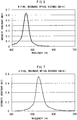
- a high-luminance B light with the sharp emission spectrum shown in FIG. 6 is emitted from the B sub-pixel region; a high-luminance G light with the sharp emission spectrum shown in FIG. 7 is emitted from the G sub-pixel region; and a high-luminance R light with the sharp emission spectrum shown in FIG. 8 is emitted from the R sub-pixel region.
- the R, G, B and W sub-pixels which are different in only the thickness of their optical path length regulation layer, are composed of the same material.
- the R, G, B and W sub-pixels have the organic electroluminescence layer and the optically semitransparent reflection layer in common, which can be consistently produced thus making formation of each pixel by separate forming unnecessary, simplifying the production process to increase productivity, and facilitating achievement of higher resolution.
- the pixel in this example corresponding to the present invention has the constitution shown in FIG. 4 which is the same as in Example 1 except that the constitution of the W sub-pixel region was changed as follows.
- the method of manufacturing each component is the same as in Example 1.
- the planarizing film 16 in the W sub-pixel region functions as a substitute for the optical path length regulation layer.
- the pixel in this non-claimed example has the constitution shown in FIG. 5 which is the same as in Example 2 except that even in the R, G and B sub-pixel regions, the light reflection layer is arranged in the planarizing film 26.
- the optical path length regulation layers in all the sub-pixel regions are arranged in the planarizing film. Accordingly, particular arrangement of the optical path length regulation layers outside the planarizing film is unnecessary, thus allowing all the R, G, B and W sub-pixel regions to be formed with the same thickness, thereby preferably planarizing the whole of the pixel with reduced depression and protrusion. Further, the transparent electrodes, the white organic electroluminescence layers or the optically semitransparent reflection layers in the sub-pixel regions can be formed of the same material in the same step, thus making the production process simple and facilitating achievement of higher resolution.
- a color display device that is capable of high-resolution color display and easily producible and a method for manufacturing the same.
- organic electroluminescence layers can be formed in common among all pixels including sub-pixels, and so the separate forming, depending on the color of emitted light, of the organic electroluminescence layer region is not necessary.
- optical path length regulation layers for forming a resonant structure can be formed of a material common among the sub-pixels by merely changing the thickness of the material.
- the optical path length regulation layer in the white sub-pixel region is thicker than the optical path length regulation layer for the red light-emitting layer, and emission of specific color is not substantially generated.
Landscapes
- Engineering & Computer Science (AREA)
- Microelectronics & Electronic Packaging (AREA)
- Physics & Mathematics (AREA)
- Optics & Photonics (AREA)
- Electroluminescent Light Sources (AREA)
- Devices For Indicating Variable Information By Combining Individual Elements (AREA)
Claims (7)
- Dispositif d'affichage en couleurs comprenant une pluralité de pixels sur un substrat, dans lequel chaque pixel comprend une pluralité de sous-pixels, les sous-pixels émettant chacun une lumière de longueur d'onde différente dans la gamme visible et comprenant en outre un sous-pixel blanc, dans lequel la pluralité de sous-pixels et le sous-pixel blanc présentent chacun une couche électroluminescente organique blanche (14) prise en sandwich entre une électrode supérieure et une électrode transparente (13) et interposée entre une couche de réflexion optiquement semi-transparente (15) et une couche de réflexion de lumière (12-1, 12-2),
la distance optique entre la couche de réflexion optiquement semi-transparente et la couche de réflexion de lumière dans chacun de la pluralité de sous-pixels forme un résonateur ayant une distance permettant de faire résonner la lumière émise, dans lequel la pluralité de sous-pixels comprend un sous-pixel rouge, un sous-pixel vert et un sous-pixel bleu, et les distances optiques entre la couche de réflexion optiquement semi-transparente (15) et la couche de réflexion de lumière (12-1) dans le sous-pixel rouge, le sous-pixel vert et le sous-pixel bleu sont les distances avec lesquelles la lumière rouge, la lumière verte et la lumière bleue sont respectivement mises en résonance,
dans lequel la distance optique entre la couche de réflexion optiquement semi-transparente (15) et la couche de réflexion de lumière (12-2) dans le sous-pixel blanc est plus longue que la distance optique maximale entre la couche de réflexion optiquement semi-transparente (15) et la couche de réflexion de lumière (12-1) dans chacun de la pluralité de sous-pixels,
dans lequel le substrat est pourvu d'un TFT connecté à l'électrode transparente (13) et présente un film de planarisation (16) sur celui-ci, et au moins l'un des sous-pixels présente un film de planarisation sur le substrat et présente la couche de réflexion de lumière sur le film de planarisation, et
dans lequel le sous-pixel rouge, le sous-pixel vert et le sous-pixel bleu présentent chacun, sur le film de planarisation, la couche de réflexion de lumière, la couche de réflexion optiquement semi-transparente et une couche de régulation de longueur de chemin optique (18-1, 18-2, 18-3) ainsi que la couche électroluminescente organique blanche interposée entre la couche de réflexion optiquement semi-transparente et la couche de réflexion de lumière, et caractérisé en ce que le sous-pixel blanc présente la couche de réflexion de lumière entre le substrat et le film de planarisation et présente, sur le film de planarisation, l'électrode transparente, la couche électroluminescente organique blanche et la couche de réflexion optiquement semi-transparente. - Dispositif d'affichage en couleurs selon la revendication 1, dans lequel la distance optique entre la couche de réflexion optiquement semi-transparente et la couche de réflexion de lumière dans le sous-pixel blanc est égale ou supérieure au double de la distance optique maximale entre la couche de réflexion optiquement semi-transparente et la couche de réflexion de lumière dans chacun de la pluralité de sous-pixels.
- Dispositif d'affichage en couleurs selon la revendication 1, dans lequel la distance optique entre la couche de réflexion optiquement semi-transparente et la couche de réflexion de lumière dans le sous-pixel blanc est égale ou supérieure à 2,0 µm.
- Dispositif d'affichage en couleurs selon la revendication 1, dans lequel la pluralité de sous-pixels et le sous-pixel blanc présentent chacun une couche électroluminescente organique blanche ayant la même composition et présentent une couche de régulation de longueur de chemin optique entre la couche de réflexion optiquement semi-transparente et la couche de réflexion de lumière, et l'épaisseur de la couche de régulation de longueur de chemin optique varie parmi les sous-pixels.
- Dispositif d'affichage en couleurs selon la revendication 1, dans lequel la couche de réflexion de lumière du sous-pixel blanc est formée au niveau d'une couche commune avec une électrode du TFT.
- Dispositif d'affichage en couleurs selon la revendication 1, dans lequel un filtre de couleur rouge, un filtre de couleur verte et un filtre de couleur bleue sont disposés du côté émission de lumière du sous-pixel émettant une lumière rouge, du sous-pixel émettant une lumière verte et du sous-pixel émettant une lumière bleue, respectivement.
- Procédé de fabrication du dispositif d'affichage en couleurs selon la revendication 1, le procédé comprenant, dans cet ordre, les étapes suivantes consistant à :1) former une couche de réflexion de lumière pour le sous-pixel blanc, sur le même substrat sur lequel le TFT a été formé,2) recouvrir le TFT pour chacun du sous-pixel émettant une lumière rouge, du sous-pixel émettant une lumière verte, du sous-pixel émettant une lumière bleue et du sous-pixel blanc, et de la couche de réflexion de lumière pour le sous-pixel blanc, pour former un film de planarisation,3) former une couche de réflexion de lumière commune au sous-pixel émettant une lumière rouge, au sous-pixel émettant une lumière verte et au sous-pixel émettant une lumière bleue,4) former les couches de régulation de longueur de chemin optique à partir d'un matériau commun au sous-pixel émettant une lumière rouge, au sous-pixel émettant une lumière verte et au sous-pixel émettant une lumière bleue en changeant l'épaisseur des couches,5) former des électrodes transparentes en tant qu'électrodes de pixel en formant un motif correspondant au sous-pixel émettant une lumière rouge, au sous-pixel émettant une lumière verte, au sous-pixel émettant une lumière bleue et au sous-pixel blanc,6) former la couche électroluminescente organique blanche commune au sous-pixel émettant une lumière rouge, au sous-pixel émettant une lumière verte, au sous-pixel émettant une lumière bleue et au sous-pixel blanc, et7) former la couche de réflexion optiquement semi-transparente commune au sous-pixel émettant une lumière rouge, au sous-pixel émettant une lumière verte, au sous-pixel émettant une lumière bleue et au sous-pixel blanc.
Priority Applications (1)
| Application Number | Priority Date | Filing Date | Title |
|---|---|---|---|
| EP20168310.9A EP3694002B1 (fr) | 2008-08-29 | 2009-08-27 | Dispositif d'affichage en couleur et son procédé de fabrication |
Applications Claiming Priority (1)
| Application Number | Priority Date | Filing Date | Title |
|---|---|---|---|
| JP2008221881A JP5117326B2 (ja) | 2008-08-29 | 2008-08-29 | カラー表示装置及びその製造方法 |
Related Child Applications (1)
| Application Number | Title | Priority Date | Filing Date |
|---|---|---|---|
| EP20168310.9A Division EP3694002B1 (fr) | 2008-08-29 | 2009-08-27 | Dispositif d'affichage en couleur et son procédé de fabrication |
Publications (3)
| Publication Number | Publication Date |
|---|---|
| EP2159843A2 EP2159843A2 (fr) | 2010-03-03 |
| EP2159843A3 EP2159843A3 (fr) | 2013-05-01 |
| EP2159843B1 true EP2159843B1 (fr) | 2020-04-15 |
Family
ID=41227059
Family Applications (2)
| Application Number | Title | Priority Date | Filing Date |
|---|---|---|---|
| EP09010980.2A Active EP2159843B1 (fr) | 2008-08-29 | 2009-08-27 | Dispositif d'affichage à couleur et son procédé de fabrication |
| EP20168310.9A Active EP3694002B1 (fr) | 2008-08-29 | 2009-08-27 | Dispositif d'affichage en couleur et son procédé de fabrication |
Family Applications After (1)
| Application Number | Title | Priority Date | Filing Date |
|---|---|---|---|
| EP20168310.9A Active EP3694002B1 (fr) | 2008-08-29 | 2009-08-27 | Dispositif d'affichage en couleur et son procédé de fabrication |
Country Status (4)
| Country | Link |
|---|---|
| US (2) | US8237360B2 (fr) |
| EP (2) | EP2159843B1 (fr) |
| JP (1) | JP5117326B2 (fr) |
| CN (1) | CN101661951B (fr) |
Families Citing this family (150)
| Publication number | Priority date | Publication date | Assignee | Title |
|---|---|---|---|---|
| JP3496147B2 (ja) | 2001-03-21 | 2004-02-09 | 有限会社ささはら | 雪害の軽減方法、及び雪庇切り落とし装置 |
| CA2419704A1 (fr) | 2003-02-24 | 2004-08-24 | Ignis Innovation Inc. | Methode de fabrication d'un pixel au moyen d'une diode electroluminescente organique |
| CA2495726A1 (fr) | 2005-01-28 | 2006-07-28 | Ignis Innovation Inc. | Pixel programme par tension a reference locale pour affichages amoled |
| US8026531B2 (en) * | 2005-03-22 | 2011-09-27 | Semiconductor Energy Laboratory Co., Ltd. | Light emitting device |
| JP5117326B2 (ja) | 2008-08-29 | 2013-01-16 | 富士フイルム株式会社 | カラー表示装置及びその製造方法 |
| JP5170020B2 (ja) * | 2008-10-03 | 2013-03-27 | セイコーエプソン株式会社 | 有機el装置及び電子機器 |
| DE102008054435A1 (de) * | 2008-12-09 | 2010-06-10 | Universität Zu Köln | Organische Leuchtdiode mit optischem Resonator nebst Herstellungsverfahren |
| JP2010232163A (ja) * | 2009-03-03 | 2010-10-14 | Fujifilm Corp | 発光表示装置の製造方法、発光表示装置、及び発光ディスプレイ |
| US8633873B2 (en) | 2009-11-12 | 2014-01-21 | Ignis Innovation Inc. | Stable fast programming scheme for displays |
| WO2011145794A1 (fr) | 2010-05-18 | 2011-11-24 | 서울반도체 주식회사 | Puce à diode électroluminescente avec couche de conversion de longueur d'onde, procédé pour sa fabrication, boîtier l'incluant et procédé pour la fabrication de celui-ci |
| JP5670178B2 (ja) | 2010-12-28 | 2015-02-18 | ユー・ディー・シー アイルランド リミテッド | 有機電界発光装置 |
| JP5617700B2 (ja) * | 2011-03-07 | 2014-11-05 | セイコーエプソン株式会社 | 発光装置および発光装置の製造方法 |
| JP5759760B2 (ja) * | 2011-03-16 | 2015-08-05 | 株式会社Joled | 表示装置および電子機器 |
| TWI562424B (en) * | 2011-03-25 | 2016-12-11 | Semiconductor Energy Lab Co Ltd | Light-emitting panel, light-emitting device, and method for manufacturing the light-emitting panel |
| US9606607B2 (en) | 2011-05-17 | 2017-03-28 | Ignis Innovation Inc. | Systems and methods for display systems with dynamic power control |
| WO2012156942A1 (fr) | 2011-05-17 | 2012-11-22 | Ignis Innovation Inc. | Systèmes et procédés pour systèmes d'affichage comprenant une commande de puissance dynamique |
| JP5741221B2 (ja) * | 2011-05-31 | 2015-07-01 | セイコーエプソン株式会社 | 発光装置および電子機器 |
| JP2013008515A (ja) * | 2011-06-23 | 2013-01-10 | Nitto Denko Corp | トップエミッション型有機エレクトロルミネッセンス素子およびその製法 |
| KR20130007167A (ko) * | 2011-06-29 | 2013-01-18 | 삼성디스플레이 주식회사 | 유기 발광 표시 장치 |
| US8901579B2 (en) | 2011-08-03 | 2014-12-02 | Ignis Innovation Inc. | Organic light emitting diode and method of manufacturing |
| US9070775B2 (en) | 2011-08-03 | 2015-06-30 | Ignis Innovations Inc. | Thin film transistor |
| KR101407309B1 (ko) * | 2011-11-15 | 2014-06-16 | 엘지디스플레이 주식회사 | 유기 전계 발광 표시 패널 및 그의 제조 방법 |
| US9385169B2 (en) | 2011-11-29 | 2016-07-05 | Ignis Innovation Inc. | Multi-functional active matrix organic light-emitting diode display |
| US10089924B2 (en) | 2011-11-29 | 2018-10-02 | Ignis Innovation Inc. | Structural and low-frequency non-uniformity compensation |
| KR101932564B1 (ko) | 2011-11-29 | 2018-12-28 | 삼성디스플레이 주식회사 | 유기 발광 표시 장치 |
| TW201324891A (zh) | 2011-12-05 | 2013-06-16 | Au Optronics Corp | 電激發光顯示面板之畫素結構 |
| TW201324758A (zh) * | 2011-12-05 | 2013-06-16 | Au Optronics Corp | 電激發光顯示面板之畫素結構 |
| KR101901832B1 (ko) | 2011-12-14 | 2018-09-28 | 삼성디스플레이 주식회사 | 유기 발광 표시 장치 및 유기 발광 표시 장치의 제조 방법 |
| WO2013099744A1 (fr) * | 2011-12-27 | 2013-07-04 | シャープ株式会社 | Dispositif d'affichage |
| TWI508279B (zh) * | 2012-01-19 | 2015-11-11 | Joled Inc | 顯示器及其製造方法,單元,轉印方法,有機電致發光單元及其製造方法,以及電子裝置 |
| TW201334622A (zh) * | 2012-02-10 | 2013-08-16 | Wintek Corp | 有機電致發光顯示裝置 |
| US9190456B2 (en) * | 2012-04-25 | 2015-11-17 | Ignis Innovation Inc. | High resolution display panel with emissive organic layers emitting light of different colors |
| KR101904466B1 (ko) * | 2012-05-08 | 2018-12-03 | 삼성디스플레이 주식회사 | 유기 발광 표시 장치 및 그 제조방법 |
| CN103545449A (zh) * | 2012-07-10 | 2014-01-29 | 群康科技(深圳)有限公司 | 有机发光二极管、包含其的显示面板及显示设备 |
| TWI506835B (zh) * | 2012-07-10 | 2015-11-01 | Innocom Tech Shenzhen Co Ltd | 有機發光二極體、包含其之顯示面板及顯示裝置 |
| KR101632298B1 (ko) * | 2012-07-16 | 2016-06-22 | 삼성디스플레이 주식회사 | 평판 표시장치 및 그 제조방법 |
| JP2014026902A (ja) * | 2012-07-30 | 2014-02-06 | Sony Corp | 表示装置、表示装置の製造方法および電子機器 |
| US8883531B2 (en) * | 2012-08-28 | 2014-11-11 | Lg Display Co., Ltd. | Organic light emitting diode display device and method of manufacturing the same |
| JP2013012493A (ja) * | 2012-09-10 | 2013-01-17 | Fujifilm Corp | カラー表示装置及びその製造方法 |
| KR101954973B1 (ko) * | 2012-09-19 | 2019-03-08 | 삼성디스플레이 주식회사 | 유기 발광 표시 장치 |
| KR101990116B1 (ko) * | 2012-10-22 | 2019-10-01 | 삼성디스플레이 주식회사 | 유기발광장치 및 그것의 제조방법 |
| US8921842B2 (en) | 2012-11-14 | 2014-12-30 | Lg Display Co., Ltd. | Organic light emitting display device and method of manufacturing the same |
| CN103000662B (zh) * | 2012-12-12 | 2014-06-18 | 京东方科技集团股份有限公司 | 阵列基板及其制作方法、显示装置 |
| KR101980758B1 (ko) * | 2012-12-14 | 2019-08-28 | 엘지디스플레이 주식회사 | Oled 표시 장치 및 그의 제조 방법 |
| JP6111643B2 (ja) * | 2012-12-17 | 2017-04-12 | セイコーエプソン株式会社 | 有機エレクトロルミネッセンス装置、及び電子機器 |
| KR101981071B1 (ko) * | 2012-12-31 | 2019-05-22 | 엘지디스플레이 주식회사 | 유기전계발광표시장치 및 그 제조방법 |
| TWI496281B (zh) * | 2013-02-05 | 2015-08-11 | Au Optronics Corp | 電激發光顯示面板之畫素結構 |
| JP2014154405A (ja) * | 2013-02-08 | 2014-08-25 | Toshiba Corp | 有機電界発光素子、照明装置及び照明システム |
| KR102037850B1 (ko) * | 2013-02-27 | 2019-10-29 | 엘지디스플레이 주식회사 | 유기 발광 표시 장치 및 그 제조 방법 |
| US9721505B2 (en) | 2013-03-08 | 2017-08-01 | Ignis Innovation Inc. | Pixel circuits for AMOLED displays |
| WO2014140992A1 (fr) | 2013-03-15 | 2014-09-18 | Ignis Innovation Inc. | Réglage dynamique des résolutions tactiles d'un écran amoled |
| JP6164402B2 (ja) * | 2013-03-27 | 2017-07-19 | セイコーエプソン株式会社 | 有機el装置の製造方法、および有機el装置 |
| CN104078574A (zh) * | 2013-03-29 | 2014-10-01 | 海洋王照明科技股份有限公司 | 有机电致发光器件及其制备方法 |
| CN104078600A (zh) * | 2013-03-29 | 2014-10-01 | 海洋王照明科技股份有限公司 | 有机电致发光器件及其制备方法 |
| TWI500146B (zh) * | 2013-04-25 | 2015-09-11 | Au Optronics Corp | 電激發光顯示面板之畫素結構 |
| CN104183742A (zh) * | 2013-05-20 | 2014-12-03 | 海洋王照明科技股份有限公司 | 一种有机电致发光器件及其制备方法 |
| JP6119437B2 (ja) | 2013-06-05 | 2017-04-26 | セイコーエプソン株式会社 | 電気光学装置、電気光学装置の製造方法、電子機器 |
| JP6221418B2 (ja) | 2013-07-01 | 2017-11-01 | セイコーエプソン株式会社 | 発光装置および電子機器 |
| KR102043853B1 (ko) * | 2013-07-24 | 2019-11-12 | 엘지디스플레이 주식회사 | 액정표시장치 |
| JP6247855B2 (ja) * | 2013-07-26 | 2017-12-13 | 株式会社ジャパンディスプレイ | 発光素子表示装置 |
| JP6286941B2 (ja) | 2013-08-27 | 2018-03-07 | セイコーエプソン株式会社 | 発光装置、発光装置の製造方法、電子機器 |
| KR102085153B1 (ko) | 2013-11-29 | 2020-03-05 | 엘지디스플레이 주식회사 | 유기 발광 장치 |
| JP6488082B2 (ja) * | 2013-12-02 | 2019-03-20 | 株式会社半導体エネルギー研究所 | 発光装置、電子機器、および照明装置 |
| KR102149199B1 (ko) * | 2013-12-19 | 2020-08-31 | 엘지디스플레이 주식회사 | 투명 디스플레이 장치 |
| US9502653B2 (en) | 2013-12-25 | 2016-11-22 | Ignis Innovation Inc. | Electrode contacts |
| CN103928495B (zh) * | 2013-12-31 | 2017-01-18 | 上海天马有机发光显示技术有限公司 | 一种oled显示面板及其制备方法、显示装置 |
| US10997901B2 (en) | 2014-02-28 | 2021-05-04 | Ignis Innovation Inc. | Display system |
| US10176752B2 (en) | 2014-03-24 | 2019-01-08 | Ignis Innovation Inc. | Integrated gate driver |
| TWI567971B (zh) * | 2014-04-22 | 2017-01-21 | 友達光電股份有限公司 | 發光裝置 |
| TWI577008B (zh) * | 2014-05-28 | 2017-04-01 | 友達光電股份有限公司 | 顯示面板 |
| CN104037202B (zh) * | 2014-06-12 | 2017-08-04 | 上海和辉光电有限公司 | 一种amoled显示器件及其子像素结构的制备方法 |
| CN104409468B (zh) | 2014-10-29 | 2018-09-14 | 京东方科技集团股份有限公司 | 显示基板及其显示装置、制作方法 |
| CN104409654A (zh) * | 2014-11-19 | 2015-03-11 | 昆山工研院新型平板显示技术中心有限公司 | 发光器件及其制备方法 |
| CA2872563A1 (fr) | 2014-11-28 | 2016-05-28 | Ignis Innovation Inc. | Architecture de reseau a densite de pixels elevee |
| CN104576694A (zh) * | 2014-12-17 | 2015-04-29 | 深圳市华星光电技术有限公司 | Oled显示装置及其制造方法 |
| CN104466027B (zh) * | 2014-12-30 | 2017-03-08 | 昆山国显光电有限公司 | 有机发光显示器的微腔结构及有机发光显示器 |
| CN104538431B (zh) * | 2014-12-31 | 2017-11-24 | 北京维信诺科技有限公司 | 一种oled器件及其制备方法、显示器 |
| CN104600097A (zh) * | 2015-02-06 | 2015-05-06 | 京东方科技集团股份有限公司 | 一种像素单元结构、有机发光显示面板及显示装置 |
| CN104716167B (zh) * | 2015-04-13 | 2017-07-25 | 京东方科技集团股份有限公司 | 一种有机电致发光显示器件、其制作方法及显示装置 |
| KR102572407B1 (ko) * | 2015-07-22 | 2023-08-30 | 엘지디스플레이 주식회사 | 박막 트랜지스터 어레이 기판 및 이를 포함하는 유기발광 표시장치 |
| US10373554B2 (en) | 2015-07-24 | 2019-08-06 | Ignis Innovation Inc. | Pixels and reference circuits and timing techniques |
| US10657895B2 (en) | 2015-07-24 | 2020-05-19 | Ignis Innovation Inc. | Pixels and reference circuits and timing techniques |
| CA2898282A1 (fr) | 2015-07-24 | 2017-01-24 | Ignis Innovation Inc. | Etalonnage hybride de sources de courant destine a des afficheurs a tension polarisee par courant programmes |
| KR102322083B1 (ko) * | 2015-07-28 | 2021-11-04 | 삼성디스플레이 주식회사 | 유기 발광 표시 장치 및 그 제조 방법 |
| KR102505166B1 (ko) * | 2015-07-30 | 2023-03-02 | 엘지디스플레이 주식회사 | 유기전계발광표시장치 |
| CN105070739B (zh) * | 2015-08-17 | 2018-06-01 | 京东方科技集团股份有限公司 | 显示背板及其制作方法、显示装置 |
| KR102396748B1 (ko) * | 2015-09-15 | 2022-05-13 | 삼성디스플레이 주식회사 | 미러 표시 장치 및 이의 제조 방법 |
| CA2909813A1 (fr) | 2015-10-26 | 2017-04-26 | Ignis Innovation Inc | Orientation de motif ppi dense |
| JP6784031B2 (ja) * | 2016-02-15 | 2020-11-11 | セイコーエプソン株式会社 | 電気光学装置、電気光学装置の製造方法、および電子機器 |
| CN105720081B (zh) * | 2016-02-24 | 2021-04-16 | 京东方科技集团股份有限公司 | 一种有机发光二极管阵列基板、显示装置和制作方法 |
| JP6731748B2 (ja) * | 2016-02-26 | 2020-07-29 | 株式会社ジャパンディスプレイ | 表示装置 |
| JP6727848B2 (ja) * | 2016-02-26 | 2020-07-22 | 株式会社ジャパンディスプレイ | 表示装置 |
| KR102603593B1 (ko) | 2016-07-29 | 2023-11-20 | 엘지디스플레이 주식회사 | 백색 발광층을 포함하는 디스플레이 장치 |
| KR102603595B1 (ko) | 2016-08-31 | 2023-11-20 | 엘지디스플레이 주식회사 | 마이크로 캐비티 구조를 갖는 디스플레이 장치 및 그의 제조 방법 |
| CN106340597B (zh) * | 2016-08-31 | 2019-01-18 | 纳晶科技股份有限公司 | 发光器件 |
| CN106324720A (zh) * | 2016-10-24 | 2017-01-11 | 昆山工研院新型平板显示技术中心有限公司 | 一种薄膜封装结构 |
| CN106373988B (zh) * | 2016-11-24 | 2019-08-02 | 上海天马有机发光显示技术有限公司 | 显示装置、有机发光显示面板及其制作方法 |
| CN108123053B (zh) * | 2016-11-29 | 2025-02-25 | 京东方科技集团股份有限公司 | 发光器件和显示装置 |
| US10586491B2 (en) | 2016-12-06 | 2020-03-10 | Ignis Innovation Inc. | Pixel circuits for mitigation of hysteresis |
| US10847744B2 (en) | 2017-03-21 | 2020-11-24 | Sony Semiconductor Solutions Corporation | Light emitting element, display device, and electronic apparatus |
| CN107146807B (zh) * | 2017-05-12 | 2019-09-06 | 京东方科技集团股份有限公司 | 像素界定层的制备方法、oled及制备方法和显示装置 |
| US10714018B2 (en) | 2017-05-17 | 2020-07-14 | Ignis Innovation Inc. | System and method for loading image correction data for displays |
| CN107195584B (zh) * | 2017-05-27 | 2020-03-31 | 广州新视界光电科技有限公司 | 一种显示面板的制备方法、显示面板及显示装置 |
| CN107154424B (zh) * | 2017-05-27 | 2019-10-18 | 广州新视界光电科技有限公司 | 一种显示面板的制备方法、显示面板及显示装置 |
| US11025899B2 (en) | 2017-08-11 | 2021-06-01 | Ignis Innovation Inc. | Optical correction systems and methods for correcting non-uniformity of emissive display devices |
| US10373936B2 (en) | 2017-08-22 | 2019-08-06 | Facebook Technologies, Llc | Pixel elements including light emitters of variable heights |
| US10373999B2 (en) | 2017-09-29 | 2019-08-06 | Taiwan Semiconductor Manufacturing Company Ltd. | Image sensor and associated fabricating method |
| JP6562054B2 (ja) * | 2017-10-02 | 2019-08-21 | セイコーエプソン株式会社 | 発光装置および電子機器 |
| KR102510569B1 (ko) * | 2017-10-27 | 2023-03-15 | 엘지디스플레이 주식회사 | 유기 발광 표시 장치 |
| KR102513910B1 (ko) * | 2017-12-18 | 2023-03-23 | 엘지디스플레이 주식회사 | 전계발광 표시장치 |
| JP2019114484A (ja) * | 2017-12-26 | 2019-07-11 | ソニーセミコンダクタソリューションズ株式会社 | 表示素子、及び電子機器 |
| CN108288636A (zh) * | 2018-01-19 | 2018-07-17 | 云谷(固安)科技有限公司 | 一种有机发光装置 |
| US10971078B2 (en) | 2018-02-12 | 2021-04-06 | Ignis Innovation Inc. | Pixel measurement through data line |
| JP7031446B2 (ja) * | 2018-03-30 | 2022-03-08 | 大日本印刷株式会社 | 有機エレクトロルミネッセンス表示装置 |
| CN110459559B (zh) * | 2018-05-07 | 2022-04-12 | 京东方科技集团股份有限公司 | 一种显示面板、其制作方法及显示装置 |
| US12225761B2 (en) * | 2018-05-11 | 2025-02-11 | Semiconductor Energy Laboratory Co., Ltd. | Display device and fabrication method thereof |
| DE102018113363A1 (de) * | 2018-06-05 | 2019-12-05 | Osram Opto Semiconductors Gmbh | Optoelektronisches bauteil und verfahren zur herstellung eines optoelektronischen bauteils |
| FR3085232B1 (fr) * | 2018-08-21 | 2020-07-17 | Commissariat A L'energie Atomique Et Aux Energies Alternatives | Pixel d’un micro-ecran a diodes electroluminescentes organiques |
| CN109742261B (zh) * | 2019-01-09 | 2021-01-22 | 昆山国显光电有限公司 | 有机发光二极管oled显示面板及显示装置 |
| JP6961109B2 (ja) * | 2019-01-15 | 2021-11-05 | ソニーセミコンダクタソリューションズ株式会社 | 表示装置、表示装置の製造方法、及び、電子機器 |
| CN110085775A (zh) * | 2019-05-07 | 2019-08-02 | 深圳市华星光电半导体显示技术有限公司 | 显示面板及其制作方法 |
| WO2020257971A1 (fr) * | 2019-06-24 | 2020-12-30 | Boe Technology Group Co., Ltd. | Substrat d'affichage, procédé de fabrication de substrat d'affichage et appareil d'affichage |
| CN110400890A (zh) * | 2019-07-26 | 2019-11-01 | 中国科学院长春光学精密机械与物理研究所 | 一种非规整微腔胶体量子点电致发光器件及其制备方法 |
| CN110459699B (zh) | 2019-08-30 | 2022-07-15 | 京东方科技集团股份有限公司 | 显示基板及其制备方法、显示装置 |
| JP7380702B2 (ja) * | 2019-11-05 | 2023-11-15 | ソニーグループ株式会社 | 表示装置 |
| CN111063831B (zh) * | 2019-12-04 | 2021-04-02 | 深圳市华星光电半导体显示技术有限公司 | Oled显示面板及其制造方法、oled显示器 |
| CN211743193U (zh) * | 2020-01-09 | 2020-10-23 | 京东方科技集团股份有限公司 | 一种阵列基板及显示装置 |
| CN111261801A (zh) | 2020-02-12 | 2020-06-09 | 武汉华星光电半导体显示技术有限公司 | 一种阵列基板及显示面板 |
| KR102785403B1 (ko) * | 2020-03-03 | 2025-03-21 | 삼성전자주식회사 | 발광 소자 및 이를 포함하는 디스플레이 장치 |
| US11758786B2 (en) | 2020-03-18 | 2023-09-12 | Boe Technology Group Co., Ltd. | Array substrate, fabricating method therefor and display panel |
| US11980046B2 (en) | 2020-05-27 | 2024-05-07 | Taiwan Semiconductor Manufacturing Company, Ltd. | Method for forming an isolation structure having multiple thicknesses to mitigate damage to a display device |
| CN111584762B (zh) * | 2020-05-28 | 2023-01-24 | 京东方科技集团股份有限公司 | 显示面板、封装方法及显示装置 |
| JP7549473B2 (ja) * | 2020-07-09 | 2024-09-11 | キヤノン株式会社 | 有機デバイス、表示装置、光電変換装置、電子機器、照明装置、移動体用の灯具および移動体 |
| KR20220018140A (ko) | 2020-08-05 | 2022-02-15 | 삼성디스플레이 주식회사 | 광조사장치 및 이의 제조방법 |
| JP7604170B2 (ja) * | 2020-10-23 | 2024-12-23 | キヤノン株式会社 | 電子デバイス、表示装置、光電変換装置、電子機器、照明、および移動体 |
| JP7614785B2 (ja) | 2020-10-28 | 2025-01-16 | キヤノン株式会社 | 発光装置、表示装置、撮像装置および電子機器、ならびに発光装置の製造方法 |
| CN112582570A (zh) * | 2020-12-09 | 2021-03-30 | 武汉华星光电半导体显示技术有限公司 | 一种显示模组 |
| TW202243238A (zh) * | 2020-12-25 | 2022-11-01 | 日商索尼半導體解決方案公司 | 顯示裝置及電子機器 |
| KR102934007B1 (ko) * | 2020-12-29 | 2026-03-04 | 엘지디스플레이 주식회사 | 표시 패널 및 이를 이용한 표시 장치 |
| KR20220124312A (ko) * | 2021-03-02 | 2022-09-14 | 삼성디스플레이 주식회사 | 표시 장치 |
| CN113193023A (zh) * | 2021-04-26 | 2021-07-30 | 睿馨(珠海)投资发展有限公司 | 一种像素单元、显示器件、显示装置及其制备方法 |
| CN115347129A (zh) * | 2021-05-13 | 2022-11-15 | 北京京东方技术开发有限公司 | 一种发光基板及发光装置 |
| CN113299858B (zh) * | 2021-05-24 | 2024-09-06 | 京东方科技集团股份有限公司 | 显示基板及其制作方法、显示装置 |
| CN113314682B (zh) * | 2021-05-27 | 2024-08-02 | 京东方科技集团股份有限公司 | 一种显示面板及其制备方法、电子设备 |
| CN113419387A (zh) * | 2021-06-22 | 2021-09-21 | 惠科股份有限公司 | 阵列基板、显示面板、显示装置及阵列基板的制备方法 |
| CN113871437A (zh) * | 2021-09-18 | 2021-12-31 | 深圳大学 | 显示器件及其制备方法和显示装置 |
| CN114864641B (zh) * | 2022-04-25 | 2026-02-17 | 合肥鑫晟光电科技有限公司 | 显示基板和显示装置 |
| CN115863508A (zh) * | 2022-12-22 | 2023-03-28 | 安徽熙泰智能科技有限公司 | 一种带有微腔的Micro LED结构及其制造方法 |
| US20240324419A1 (en) * | 2023-03-24 | 2024-09-26 | Samsung Display Co., Ltd. | Display apparatus |
| CN121816856A (zh) * | 2024-07-24 | 2026-04-07 | 京东方科技集团股份有限公司 | 阵列基板、显示装置和制造阵列基板的方法 |
Family Cites Families (23)
| Publication number | Priority date | Publication date | Assignee | Title |
|---|---|---|---|---|
| US4885211A (en) | 1987-02-11 | 1989-12-05 | Eastman Kodak Company | Electroluminescent device with improved cathode |
| US4996523A (en) | 1988-10-20 | 1991-02-26 | Eastman Kodak Company | Electroluminescent storage display with improved intensity driver circuits |
| JP2780880B2 (ja) | 1990-11-28 | 1998-07-30 | 出光興産株式会社 | 有機エレクトロルミネッセンス素子および該素子を用いた発光装置 |
| JP3236332B2 (ja) | 1991-01-29 | 2001-12-10 | パイオニア株式会社 | 有機エレクトロルミネッセンス素子 |
| JP2784615B2 (ja) | 1991-10-16 | 1998-08-06 | 株式会社半導体エネルギー研究所 | 電気光学表示装置およびその駆動方法 |
| JP3063453B2 (ja) | 1993-04-16 | 2000-07-12 | 凸版印刷株式会社 | 有機薄膜el素子の駆動方法 |
| JPH07134558A (ja) | 1993-11-08 | 1995-05-23 | Idemitsu Kosan Co Ltd | 有機エレクトロルミネッセンス表示装置 |
| US5550066A (en) | 1994-12-14 | 1996-08-27 | Eastman Kodak Company | Method of fabricating a TFT-EL pixel |
| US6137467A (en) | 1995-01-03 | 2000-10-24 | Xerox Corporation | Optically sensitive electric paper |
| JP4046948B2 (ja) * | 2001-02-26 | 2008-02-13 | 株式会社日立製作所 | 有機発光表示装置 |
| US7030553B2 (en) * | 2003-08-19 | 2006-04-18 | Eastman Kodak Company | OLED device having microcavity gamut subpixels and a within gamut subpixel |
| US7129634B2 (en) * | 2004-04-07 | 2006-10-31 | Eastman Kodak Company | Color OLED with added color gamut pixels |
| JP4742639B2 (ja) * | 2005-03-25 | 2011-08-10 | セイコーエプソン株式会社 | 発光装置 |
| JP2007005173A (ja) * | 2005-06-24 | 2007-01-11 | Toshiba Matsushita Display Technology Co Ltd | 表示装置 |
| JP2007059116A (ja) * | 2005-08-23 | 2007-03-08 | Sony Corp | 表示装置 |
| JP2007108249A (ja) * | 2005-10-11 | 2007-04-26 | Sony Corp | 表示装置及びその駆動方法 |
| JP2007108248A (ja) * | 2005-10-11 | 2007-04-26 | Sony Corp | 表示装置 |
| JP2007141789A (ja) * | 2005-11-22 | 2007-06-07 | Sanyo Electric Co Ltd | 発光素子および表示装置 |
| TW200721896A (en) | 2005-11-22 | 2007-06-01 | Sanyo Electric Co | Light emitting element and display device |
| TW200803606A (en) * | 2006-06-13 | 2008-01-01 | Itc Inc Ltd | The fabrication of full color OLED panel using micro-cavity structure |
| JP4816354B2 (ja) * | 2006-09-15 | 2011-11-16 | セイコーエプソン株式会社 | 電気光学装置及び電子機器 |
| US7859188B2 (en) * | 2007-08-21 | 2010-12-28 | Global Oled Technology Llc | LED device having improved contrast |
| JP5117326B2 (ja) | 2008-08-29 | 2013-01-16 | 富士フイルム株式会社 | カラー表示装置及びその製造方法 |
-
2008
- 2008-08-29 JP JP2008221881A patent/JP5117326B2/ja active Active
-
2009
- 2009-08-20 US US12/544,239 patent/US8237360B2/en active Active
- 2009-08-26 CN CN2009101704523A patent/CN101661951B/zh active Active
- 2009-08-27 EP EP09010980.2A patent/EP2159843B1/fr active Active
- 2009-08-27 EP EP20168310.9A patent/EP3694002B1/fr active Active
-
2012
- 2012-08-06 US US13/567,094 patent/US8513882B2/en active Active
Non-Patent Citations (1)
| Title |
|---|
| None * |
Also Published As
| Publication number | Publication date |
|---|---|
| EP3694002A1 (fr) | 2020-08-12 |
| US8237360B2 (en) | 2012-08-07 |
| JP2010056017A (ja) | 2010-03-11 |
| US20100052524A1 (en) | 2010-03-04 |
| EP3694002B1 (fr) | 2025-10-01 |
| CN101661951B (zh) | 2011-06-15 |
| US20120299002A1 (en) | 2012-11-29 |
| US8513882B2 (en) | 2013-08-20 |
| JP5117326B2 (ja) | 2013-01-16 |
| EP2159843A2 (fr) | 2010-03-03 |
| CN101661951A (zh) | 2010-03-03 |
| EP2159843A3 (fr) | 2013-05-01 |
Similar Documents
| Publication | Publication Date | Title |
|---|---|---|
| EP2159843B1 (fr) | Dispositif d'affichage à couleur et son procédé de fabrication | |
| JP5918340B2 (ja) | カラー表示装置及びその製造方法 | |
| US20100053038A1 (en) | Color display and method for producing the same | |
| US20100053043A1 (en) | Color display and method for producing the same | |
| JP2010056015A (ja) | 表示装置及びその製造方法 | |
| US10510973B2 (en) | Color-stable organic light emitting diode stack | |
| US7728517B2 (en) | Intermediate electrodes for stacked OLEDs | |
| US7750561B2 (en) | Stacked OLED structure | |
| JP4281308B2 (ja) | 多色発光装置及びその製造方法 | |
| JP2013012493A (ja) | カラー表示装置及びその製造方法 | |
| US12588382B2 (en) | Color stable multicolor OLED device structures | |
| GB2416919A (en) | Liquid electrodes for organic semiconductor devices | |
| JP5052464B2 (ja) | 有機電界発光表示装置の製造方法 | |
| US20020122900A1 (en) | Organic electroluminescent device and display unit | |
| JPH11329731A (ja) | 有機電界発光素子 | |
| JP2000091073A (ja) | 有機電界発光素子 | |
| US7453204B2 (en) | Light emitting element with light-emitting material in different concentrations | |
| JP2000012226A (ja) | 有機電界発光素子 | |
| JP2000091077A (ja) | 有機電界発光素子 | |
| JPH11329730A (ja) | 有機電界発光素子 | |
| JP2008225101A (ja) | 表示装置 | |
| JP2005005226A (ja) | 有機電界発光素子 | |
| JP2000012225A (ja) | 有機電界発光素子 | |
| US20070145894A1 (en) | Organic electroluminescence device and producing method thereof | |
| JP2000012228A (ja) | 有機電界発光素子 |
Legal Events
| Date | Code | Title | Description |
|---|---|---|---|
| PUAI | Public reference made under article 153(3) epc to a published international application that has entered the european phase |
Free format text: ORIGINAL CODE: 0009012 |
|
| AK | Designated contracting states |
Kind code of ref document: A2 Designated state(s): AT BE BG CH CY CZ DE DK EE ES FI FR GB GR HR HU IE IS IT LI LT LU LV MC MK MT NL NO PL PT RO SE SI SK SM TR |
|
| AX | Request for extension of the european patent |
Extension state: AL BA RS |
|
| RAP1 | Party data changed (applicant data changed or rights of an application transferred) |
Owner name: UDC IRELAND LIMITED |
|
| PUAL | Search report despatched |
Free format text: ORIGINAL CODE: 0009013 |
|
| AK | Designated contracting states |
Kind code of ref document: A3 Designated state(s): AT BE BG CH CY CZ DE DK EE ES FI FR GB GR HR HU IE IS IT LI LT LU LV MC MK MT NL NO PL PT RO SE SI SK SM TR |
|
| AX | Request for extension of the european patent |
Extension state: AL BA RS |
|
| RIC1 | Information provided on ipc code assigned before grant |
Ipc: H01L 27/32 20060101AFI20130327BHEP Ipc: H01L 51/52 20060101ALI20130327BHEP |
|
| RBV | Designated contracting states (corrected) |
Designated state(s): AT BE BG CH CY CZ DE DK EE ES FI FR GB GR HR HU IE IS IT LI LT LU LV MC MK MT NL NO PL PT RO SE SI SK SM TR |
|
| 17P | Request for examination filed |
Effective date: 20131104 |
|
| 17Q | First examination report despatched |
Effective date: 20150914 |
|
| RAP1 | Party data changed (applicant data changed or rights of an application transferred) |
Owner name: UDC IRELAND LIMITED |
|
| STAA | Information on the status of an ep patent application or granted ep patent |
Free format text: STATUS: EXAMINATION IS IN PROGRESS |
|
| GRAP | Despatch of communication of intention to grant a patent |
Free format text: ORIGINAL CODE: EPIDOSNIGR1 |
|
| STAA | Information on the status of an ep patent application or granted ep patent |
Free format text: STATUS: GRANT OF PATENT IS INTENDED |
|
| INTG | Intention to grant announced |
Effective date: 20190710 |
|
| GRAJ | Information related to disapproval of communication of intention to grant by the applicant or resumption of examination proceedings by the epo deleted |
Free format text: ORIGINAL CODE: EPIDOSDIGR1 |
|
| STAA | Information on the status of an ep patent application or granted ep patent |
Free format text: STATUS: EXAMINATION IS IN PROGRESS |
|
| INTC | Intention to grant announced (deleted) | ||
| GRAP | Despatch of communication of intention to grant a patent |
Free format text: ORIGINAL CODE: EPIDOSNIGR1 |
|
| STAA | Information on the status of an ep patent application or granted ep patent |
Free format text: STATUS: GRANT OF PATENT IS INTENDED |
|
| INTG | Intention to grant announced |
Effective date: 20191202 |
|
| GRAS | Grant fee paid |
Free format text: ORIGINAL CODE: EPIDOSNIGR3 |
|
| GRAA | (expected) grant |
Free format text: ORIGINAL CODE: 0009210 |
|
| STAA | Information on the status of an ep patent application or granted ep patent |
Free format text: STATUS: THE PATENT HAS BEEN GRANTED |
|
| AK | Designated contracting states |
Kind code of ref document: B1 Designated state(s): AT BE BG CH CY CZ DE DK EE ES FI FR GB GR HR HU IE IS IT LI LT LU LV MC MK MT NL NO PL PT RO SE SI SK SM TR |
|
| REG | Reference to a national code |
Ref country code: GB Ref legal event code: FG4D Ref country code: CH Ref legal event code: EP |
|
| REG | Reference to a national code |
Ref country code: DE Ref legal event code: R096 Ref document number: 602009061717 Country of ref document: DE |
|
| REG | Reference to a national code |
Ref country code: IE Ref legal event code: FG4D |
|
| REG | Reference to a national code |
Ref country code: AT Ref legal event code: REF Ref document number: 1258302 Country of ref document: AT Kind code of ref document: T Effective date: 20200515 |
|
| REG | Reference to a national code |
Ref country code: NL Ref legal event code: MP Effective date: 20200415 |
|
| REG | Reference to a national code |
Ref country code: LT Ref legal event code: MG4D |
|
| PG25 | Lapsed in a contracting state [announced via postgrant information from national office to epo] |
Ref country code: NO Free format text: LAPSE BECAUSE OF FAILURE TO SUBMIT A TRANSLATION OF THE DESCRIPTION OR TO PAY THE FEE WITHIN THE PRESCRIBED TIME-LIMIT Effective date: 20200715 Ref country code: IS Free format text: LAPSE BECAUSE OF FAILURE TO SUBMIT A TRANSLATION OF THE DESCRIPTION OR TO PAY THE FEE WITHIN THE PRESCRIBED TIME-LIMIT Effective date: 20200815 Ref country code: PT Free format text: LAPSE BECAUSE OF FAILURE TO SUBMIT A TRANSLATION OF THE DESCRIPTION OR TO PAY THE FEE WITHIN THE PRESCRIBED TIME-LIMIT Effective date: 20200817 Ref country code: FI Free format text: LAPSE BECAUSE OF FAILURE TO SUBMIT A TRANSLATION OF THE DESCRIPTION OR TO PAY THE FEE WITHIN THE PRESCRIBED TIME-LIMIT Effective date: 20200415 Ref country code: GR Free format text: LAPSE BECAUSE OF FAILURE TO SUBMIT A TRANSLATION OF THE DESCRIPTION OR TO PAY THE FEE WITHIN THE PRESCRIBED TIME-LIMIT Effective date: 20200716 Ref country code: NL Free format text: LAPSE BECAUSE OF FAILURE TO SUBMIT A TRANSLATION OF THE DESCRIPTION OR TO PAY THE FEE WITHIN THE PRESCRIBED TIME-LIMIT Effective date: 20200415 Ref country code: LT Free format text: LAPSE BECAUSE OF FAILURE TO SUBMIT A TRANSLATION OF THE DESCRIPTION OR TO PAY THE FEE WITHIN THE PRESCRIBED TIME-LIMIT Effective date: 20200415 Ref country code: SE Free format text: LAPSE BECAUSE OF FAILURE TO SUBMIT A TRANSLATION OF THE DESCRIPTION OR TO PAY THE FEE WITHIN THE PRESCRIBED TIME-LIMIT Effective date: 20200415 |
|
| REG | Reference to a national code |
Ref country code: AT Ref legal event code: MK05 Ref document number: 1258302 Country of ref document: AT Kind code of ref document: T Effective date: 20200415 |
|
| PG25 | Lapsed in a contracting state [announced via postgrant information from national office to epo] |
Ref country code: BG Free format text: LAPSE BECAUSE OF FAILURE TO SUBMIT A TRANSLATION OF THE DESCRIPTION OR TO PAY THE FEE WITHIN THE PRESCRIBED TIME-LIMIT Effective date: 20200715 Ref country code: HR Free format text: LAPSE BECAUSE OF FAILURE TO SUBMIT A TRANSLATION OF THE DESCRIPTION OR TO PAY THE FEE WITHIN THE PRESCRIBED TIME-LIMIT Effective date: 20200415 Ref country code: LV Free format text: LAPSE BECAUSE OF FAILURE TO SUBMIT A TRANSLATION OF THE DESCRIPTION OR TO PAY THE FEE WITHIN THE PRESCRIBED TIME-LIMIT Effective date: 20200415 |
|
| REG | Reference to a national code |
Ref country code: DE Ref legal event code: R097 Ref document number: 602009061717 Country of ref document: DE |
|
| PG25 | Lapsed in a contracting state [announced via postgrant information from national office to epo] |
Ref country code: DK Free format text: LAPSE BECAUSE OF FAILURE TO SUBMIT A TRANSLATION OF THE DESCRIPTION OR TO PAY THE FEE WITHIN THE PRESCRIBED TIME-LIMIT Effective date: 20200415 Ref country code: SM Free format text: LAPSE BECAUSE OF FAILURE TO SUBMIT A TRANSLATION OF THE DESCRIPTION OR TO PAY THE FEE WITHIN THE PRESCRIBED TIME-LIMIT Effective date: 20200415 Ref country code: IT Free format text: LAPSE BECAUSE OF FAILURE TO SUBMIT A TRANSLATION OF THE DESCRIPTION OR TO PAY THE FEE WITHIN THE PRESCRIBED TIME-LIMIT Effective date: 20200415 Ref country code: AT Free format text: LAPSE BECAUSE OF FAILURE TO SUBMIT A TRANSLATION OF THE DESCRIPTION OR TO PAY THE FEE WITHIN THE PRESCRIBED TIME-LIMIT Effective date: 20200415 Ref country code: EE Free format text: LAPSE BECAUSE OF FAILURE TO SUBMIT A TRANSLATION OF THE DESCRIPTION OR TO PAY THE FEE WITHIN THE PRESCRIBED TIME-LIMIT Effective date: 20200415 Ref country code: ES Free format text: LAPSE BECAUSE OF FAILURE TO SUBMIT A TRANSLATION OF THE DESCRIPTION OR TO PAY THE FEE WITHIN THE PRESCRIBED TIME-LIMIT Effective date: 20200415 Ref country code: CZ Free format text: LAPSE BECAUSE OF FAILURE TO SUBMIT A TRANSLATION OF THE DESCRIPTION OR TO PAY THE FEE WITHIN THE PRESCRIBED TIME-LIMIT Effective date: 20200415 Ref country code: RO Free format text: LAPSE BECAUSE OF FAILURE TO SUBMIT A TRANSLATION OF THE DESCRIPTION OR TO PAY THE FEE WITHIN THE PRESCRIBED TIME-LIMIT Effective date: 20200415 |
|
| PLBE | No opposition filed within time limit |
Free format text: ORIGINAL CODE: 0009261 |
|
| STAA | Information on the status of an ep patent application or granted ep patent |
Free format text: STATUS: NO OPPOSITION FILED WITHIN TIME LIMIT |
|
| PG25 | Lapsed in a contracting state [announced via postgrant information from national office to epo] |
Ref country code: PL Free format text: LAPSE BECAUSE OF FAILURE TO SUBMIT A TRANSLATION OF THE DESCRIPTION OR TO PAY THE FEE WITHIN THE PRESCRIBED TIME-LIMIT Effective date: 20200415 Ref country code: SK Free format text: LAPSE BECAUSE OF FAILURE TO SUBMIT A TRANSLATION OF THE DESCRIPTION OR TO PAY THE FEE WITHIN THE PRESCRIBED TIME-LIMIT Effective date: 20200415 |
|
| 26N | No opposition filed |
Effective date: 20210118 |
|
| PG25 | Lapsed in a contracting state [announced via postgrant information from national office to epo] |
Ref country code: MC Free format text: LAPSE BECAUSE OF FAILURE TO SUBMIT A TRANSLATION OF THE DESCRIPTION OR TO PAY THE FEE WITHIN THE PRESCRIBED TIME-LIMIT Effective date: 20200415 |
|
| REG | Reference to a national code |
Ref country code: CH Ref legal event code: PL |
|
| PG25 | Lapsed in a contracting state [announced via postgrant information from national office to epo] |
Ref country code: LU Free format text: LAPSE BECAUSE OF NON-PAYMENT OF DUE FEES Effective date: 20200827 Ref country code: LI Free format text: LAPSE BECAUSE OF NON-PAYMENT OF DUE FEES Effective date: 20200831 Ref country code: CH Free format text: LAPSE BECAUSE OF NON-PAYMENT OF DUE FEES Effective date: 20200831 |
|
| REG | Reference to a national code |
Ref country code: BE Ref legal event code: MM Effective date: 20200831 |
|
| PG25 | Lapsed in a contracting state [announced via postgrant information from national office to epo] |
Ref country code: SI Free format text: LAPSE BECAUSE OF FAILURE TO SUBMIT A TRANSLATION OF THE DESCRIPTION OR TO PAY THE FEE WITHIN THE PRESCRIBED TIME-LIMIT Effective date: 20200415 |
|
| PG25 | Lapsed in a contracting state [announced via postgrant information from national office to epo] |
Ref country code: IE Free format text: LAPSE BECAUSE OF NON-PAYMENT OF DUE FEES Effective date: 20200827 Ref country code: BE Free format text: LAPSE BECAUSE OF NON-PAYMENT OF DUE FEES Effective date: 20200831 |
|
| PG25 | Lapsed in a contracting state [announced via postgrant information from national office to epo] |
Ref country code: TR Free format text: LAPSE BECAUSE OF FAILURE TO SUBMIT A TRANSLATION OF THE DESCRIPTION OR TO PAY THE FEE WITHIN THE PRESCRIBED TIME-LIMIT Effective date: 20200415 Ref country code: MT Free format text: LAPSE BECAUSE OF FAILURE TO SUBMIT A TRANSLATION OF THE DESCRIPTION OR TO PAY THE FEE WITHIN THE PRESCRIBED TIME-LIMIT Effective date: 20200415 Ref country code: CY Free format text: LAPSE BECAUSE OF FAILURE TO SUBMIT A TRANSLATION OF THE DESCRIPTION OR TO PAY THE FEE WITHIN THE PRESCRIBED TIME-LIMIT Effective date: 20200415 |
|
| PG25 | Lapsed in a contracting state [announced via postgrant information from national office to epo] |
Ref country code: MK Free format text: LAPSE BECAUSE OF FAILURE TO SUBMIT A TRANSLATION OF THE DESCRIPTION OR TO PAY THE FEE WITHIN THE PRESCRIBED TIME-LIMIT Effective date: 20200415 |
|
| REG | Reference to a national code |
Ref country code: DE Ref legal event code: R079 Ref document number: 602009061717 Country of ref document: DE Free format text: PREVIOUS MAIN CLASS: H01L0027320000 Ipc: H10K0059000000 |
|
| P01 | Opt-out of the competence of the unified patent court (upc) registered |
Effective date: 20230426 |
|
| PGFP | Annual fee paid to national office [announced via postgrant information from national office to epo] |
Ref country code: DE Payment date: 20250827 Year of fee payment: 17 |
|
| PGFP | Annual fee paid to national office [announced via postgrant information from national office to epo] |
Ref country code: GB Payment date: 20250827 Year of fee payment: 17 |
|
| PGFP | Annual fee paid to national office [announced via postgrant information from national office to epo] |
Ref country code: FR Payment date: 20250825 Year of fee payment: 17 |