EP2174535B1 - Procédé permettant de fournir une traversée électrique hermétique - Google Patents
Procédé permettant de fournir une traversée électrique hermétique Download PDFInfo
- Publication number
- EP2174535B1 EP2174535B1 EP07871188.4A EP07871188A EP2174535B1 EP 2174535 B1 EP2174535 B1 EP 2174535B1 EP 07871188 A EP07871188 A EP 07871188A EP 2174535 B1 EP2174535 B1 EP 2174535B1
- Authority
- EP
- European Patent Office
- Prior art keywords
- ceramic sheet
- ceramic
- paste
- sheet
- via hole
- Prior art date
- Legal status (The legal status is an assumption and is not a legal conclusion. Google has not performed a legal analysis and makes no representation as to the accuracy of the status listed.)
- Active
Links
- 238000000034 method Methods 0.000 title claims description 47
- 239000000919 ceramic Substances 0.000 claims description 106
- 239000000758 substrate Substances 0.000 claims description 44
- 239000000463 material Substances 0.000 claims description 17
- 238000010304 firing Methods 0.000 claims description 15
- TWNQGVIAIRXVLR-UHFFFAOYSA-N oxo(oxoalumanyloxy)alumane Chemical compound O=[Al]O[Al]=O TWNQGVIAIRXVLR-UHFFFAOYSA-N 0.000 claims description 11
- BASFCYQUMIYNBI-UHFFFAOYSA-N platinum Chemical compound [Pt] BASFCYQUMIYNBI-UHFFFAOYSA-N 0.000 claims description 10
- 229910010293 ceramic material Inorganic materials 0.000 claims description 9
- 238000004519 manufacturing process Methods 0.000 claims description 9
- 238000005245 sintering Methods 0.000 claims description 7
- 229910052751 metal Inorganic materials 0.000 claims description 6
- 239000002184 metal Substances 0.000 claims description 6
- 238000010030 laminating Methods 0.000 claims description 5
- 229910052697 platinum Inorganic materials 0.000 claims description 5
- 239000002904 solvent Substances 0.000 claims description 5
- PCHJSUWPFVWCPO-UHFFFAOYSA-N gold Chemical compound [Au] PCHJSUWPFVWCPO-UHFFFAOYSA-N 0.000 claims description 4
- 229910052737 gold Inorganic materials 0.000 claims description 4
- 239000010931 gold Substances 0.000 claims description 4
- 239000000203 mixture Substances 0.000 claims description 4
- RTAQQCXQSZGOHL-UHFFFAOYSA-N Titanium Chemical compound [Ti] RTAQQCXQSZGOHL-UHFFFAOYSA-N 0.000 claims description 3
- 238000005530 etching Methods 0.000 claims description 3
- 229910052719 titanium Inorganic materials 0.000 claims description 3
- 239000010936 titanium Substances 0.000 claims description 3
- 239000011230 binding agent Substances 0.000 claims description 2
- 230000008020 evaporation Effects 0.000 claims description 2
- 238000001704 evaporation Methods 0.000 claims description 2
- 238000000608 laser ablation Methods 0.000 claims description 2
- 229910052758 niobium Inorganic materials 0.000 claims description 2
- 239000010955 niobium Substances 0.000 claims description 2
- GUCVJGMIXFAOAE-UHFFFAOYSA-N niobium atom Chemical compound [Nb] GUCVJGMIXFAOAE-UHFFFAOYSA-N 0.000 claims description 2
- 229910000510 noble metal Inorganic materials 0.000 claims description 2
- 239000003870 refractory metal Substances 0.000 claims description 2
- 229910052715 tantalum Inorganic materials 0.000 claims description 2
- GUVRBAGPIYLISA-UHFFFAOYSA-N tantalum atom Chemical compound [Ta] GUVRBAGPIYLISA-UHFFFAOYSA-N 0.000 claims description 2
- KDLHZDBZIXYQEI-UHFFFAOYSA-N Palladium Chemical compound [Pd] KDLHZDBZIXYQEI-UHFFFAOYSA-N 0.000 claims 2
- 238000005553 drilling Methods 0.000 claims 1
- RVTZCBVAJQQJTK-UHFFFAOYSA-N oxygen(2-);zirconium(4+) Chemical compound [O-2].[O-2].[Zr+4] RVTZCBVAJQQJTK-UHFFFAOYSA-N 0.000 claims 1
- 229910052763 palladium Inorganic materials 0.000 claims 1
- 238000004080 punching Methods 0.000 claims 1
- 229910001928 zirconium oxide Inorganic materials 0.000 claims 1
- 230000008569 process Effects 0.000 description 10
- 238000003475 lamination Methods 0.000 description 4
- 238000007639 printing Methods 0.000 description 4
- 239000000243 solution Substances 0.000 description 4
- 238000013459 approach Methods 0.000 description 3
- 238000000429 assembly Methods 0.000 description 3
- 230000000712 assembly Effects 0.000 description 3
- 230000006835 compression Effects 0.000 description 3
- 238000007906 compression Methods 0.000 description 3
- 238000009792 diffusion process Methods 0.000 description 3
- 238000000227 grinding Methods 0.000 description 3
- 238000002513 implantation Methods 0.000 description 3
- 239000002245 particle Substances 0.000 description 3
- 238000005275 alloying Methods 0.000 description 2
- 230000015572 biosynthetic process Effects 0.000 description 2
- 238000013329 compounding Methods 0.000 description 2
- 150000001875 compounds Chemical class 0.000 description 2
- 239000004020 conductor Substances 0.000 description 2
- 238000007596 consolidation process Methods 0.000 description 2
- 230000002939 deleterious effect Effects 0.000 description 2
- 238000000280 densification Methods 0.000 description 2
- -1 e.g. Inorganic materials 0.000 description 2
- 238000012360 testing method Methods 0.000 description 2
- 238000009736 wetting Methods 0.000 description 2
- QCWXUUIWCKQGHC-UHFFFAOYSA-N Zirconium Chemical compound [Zr] QCWXUUIWCKQGHC-UHFFFAOYSA-N 0.000 description 1
- 230000009471 action Effects 0.000 description 1
- 239000000956 alloy Substances 0.000 description 1
- 229910045601 alloy Inorganic materials 0.000 description 1
- 230000004888 barrier function Effects 0.000 description 1
- 230000008901 benefit Effects 0.000 description 1
- 238000005219 brazing Methods 0.000 description 1
- 238000001816 cooling Methods 0.000 description 1
- 239000013078 crystal Substances 0.000 description 1
- 238000011161 development Methods 0.000 description 1
- 238000010586 diagram Methods 0.000 description 1
- 239000000156 glass melt Substances 0.000 description 1
- 230000036541 health Effects 0.000 description 1
- 238000010438 heat treatment Methods 0.000 description 1
- 229910052734 helium Inorganic materials 0.000 description 1
- 239000001307 helium Substances 0.000 description 1
- SWQJXJOGLNCZEY-UHFFFAOYSA-N helium atom Chemical compound [He] SWQJXJOGLNCZEY-UHFFFAOYSA-N 0.000 description 1
- 239000010954 inorganic particle Substances 0.000 description 1
- 230000007246 mechanism Effects 0.000 description 1
- 230000008018 melting Effects 0.000 description 1
- 238000002844 melting Methods 0.000 description 1
- 238000004377 microelectronic Methods 0.000 description 1
- 238000012986 modification Methods 0.000 description 1
- 230000004048 modification Effects 0.000 description 1
- 238000004806 packaging method and process Methods 0.000 description 1
- 238000005498 polishing Methods 0.000 description 1
- 239000000843 powder Substances 0.000 description 1
- 238000004663 powder metallurgy Methods 0.000 description 1
- 238000011160 research Methods 0.000 description 1
- 239000011347 resin Substances 0.000 description 1
- 229920005989 resin Polymers 0.000 description 1
- 238000007789 sealing Methods 0.000 description 1
- 239000006104 solid solution Substances 0.000 description 1
- 238000007711 solidification Methods 0.000 description 1
- 230000008023 solidification Effects 0.000 description 1
- 239000000126 substance Substances 0.000 description 1
- 239000000725 suspension Substances 0.000 description 1
- 229910052726 zirconium Inorganic materials 0.000 description 1
Images




Classifications
-
- H—ELECTRICITY
- H05—ELECTRIC TECHNIQUES NOT OTHERWISE PROVIDED FOR
- H05K—PRINTED CIRCUITS; CASINGS OR CONSTRUCTIONAL DETAILS OF ELECTRIC APPARATUS; MANUFACTURE OF ASSEMBLAGES OF ELECTRICAL COMPONENTS
- H05K3/00—Apparatus or processes for manufacturing printed circuits
- H05K3/40—Forming printed elements for providing electric connections to or between printed circuits
- H05K3/4038—Through-connections; Vertical interconnect access [VIA] connections
- H05K3/4053—Through-connections; Vertical interconnect access [VIA] connections by thick-film techniques
- H05K3/4061—Through-connections; Vertical interconnect access [VIA] connections by thick-film techniques for via connections in inorganic insulating substrates
-
- B—PERFORMING OPERATIONS; TRANSPORTING
- B32—LAYERED PRODUCTS
- B32B—LAYERED PRODUCTS, i.e. PRODUCTS BUILT-UP OF STRATA OF FLAT OR NON-FLAT, e.g. CELLULAR OR HONEYCOMB, FORM
- B32B37/00—Methods or apparatus for laminating, e.g. by curing or by ultrasonic bonding
- B32B37/14—Methods or apparatus for laminating, e.g. by curing or by ultrasonic bonding characterised by the properties of the layers
-
- C—CHEMISTRY; METALLURGY
- C04—CEMENTS; CONCRETE; ARTIFICIAL STONE; CERAMICS; REFRACTORIES
- C04B—LIME, MAGNESIA; SLAG; CEMENTS; COMPOSITIONS THEREOF, e.g. MORTARS, CONCRETE OR LIKE BUILDING MATERIALS; ARTIFICIAL STONE; CERAMICS; REFRACTORIES; TREATMENT OF NATURAL STONE
- C04B35/00—Shaped ceramic products characterised by their composition; Ceramics compositions; Processing powders of inorganic compounds preparatory to the manufacturing of ceramic products
- C04B35/01—Shaped ceramic products characterised by their composition; Ceramics compositions; Processing powders of inorganic compounds preparatory to the manufacturing of ceramic products based on oxide ceramics
- C04B35/10—Shaped ceramic products characterised by their composition; Ceramics compositions; Processing powders of inorganic compounds preparatory to the manufacturing of ceramic products based on oxide ceramics based on aluminium oxide
-
- C—CHEMISTRY; METALLURGY
- C04—CEMENTS; CONCRETE; ARTIFICIAL STONE; CERAMICS; REFRACTORIES
- C04B—LIME, MAGNESIA; SLAG; CEMENTS; COMPOSITIONS THEREOF, e.g. MORTARS, CONCRETE OR LIKE BUILDING MATERIALS; ARTIFICIAL STONE; CERAMICS; REFRACTORIES; TREATMENT OF NATURAL STONE
- C04B37/00—Joining burned ceramic articles with other burned ceramic articles or other articles by heating
-
- H—ELECTRICITY
- H05—ELECTRIC TECHNIQUES NOT OTHERWISE PROVIDED FOR
- H05K—PRINTED CIRCUITS; CASINGS OR CONSTRUCTIONAL DETAILS OF ELECTRIC APPARATUS; MANUFACTURE OF ASSEMBLAGES OF ELECTRICAL COMPONENTS
- H05K3/00—Apparatus or processes for manufacturing printed circuits
- H05K3/0011—Working of insulating substrates or insulating layers
- H05K3/0044—Mechanical working of the substrate, e.g. drilling or punching
-
- H—ELECTRICITY
- H05—ELECTRIC TECHNIQUES NOT OTHERWISE PROVIDED FOR
- H05K—PRINTED CIRCUITS; CASINGS OR CONSTRUCTIONAL DETAILS OF ELECTRIC APPARATUS; MANUFACTURE OF ASSEMBLAGES OF ELECTRICAL COMPONENTS
- H05K3/00—Apparatus or processes for manufacturing printed circuits
- H05K3/0011—Working of insulating substrates or insulating layers
- H05K3/0044—Mechanical working of the substrate, e.g. drilling or punching
- H05K3/0047—Drilling of holes
-
- H—ELECTRICITY
- H05—ELECTRIC TECHNIQUES NOT OTHERWISE PROVIDED FOR
- H05K—PRINTED CIRCUITS; CASINGS OR CONSTRUCTIONAL DETAILS OF ELECTRIC APPARATUS; MANUFACTURE OF ASSEMBLAGES OF ELECTRICAL COMPONENTS
- H05K3/00—Apparatus or processes for manufacturing printed circuits
- H05K3/0011—Working of insulating substrates or insulating layers
- H05K3/0044—Mechanical working of the substrate, e.g. drilling or punching
- H05K3/005—Punching of holes
-
- H—ELECTRICITY
- H05—ELECTRIC TECHNIQUES NOT OTHERWISE PROVIDED FOR
- H05K—PRINTED CIRCUITS; CASINGS OR CONSTRUCTIONAL DETAILS OF ELECTRIC APPARATUS; MANUFACTURE OF ASSEMBLAGES OF ELECTRICAL COMPONENTS
- H05K3/00—Apparatus or processes for manufacturing printed circuits
- H05K3/10—Apparatus or processes for manufacturing printed circuits in which conductive material is applied to the insulating support in such a manner as to form the desired conductive pattern
- H05K3/12—Apparatus or processes for manufacturing printed circuits in which conductive material is applied to the insulating support in such a manner as to form the desired conductive pattern using thick film techniques, e.g. printing techniques to apply the conductive material or similar techniques for applying conductive paste or ink patterns
-
- H—ELECTRICITY
- H05—ELECTRIC TECHNIQUES NOT OTHERWISE PROVIDED FOR
- H05K—PRINTED CIRCUITS; CASINGS OR CONSTRUCTIONAL DETAILS OF ELECTRIC APPARATUS; MANUFACTURE OF ASSEMBLAGES OF ELECTRICAL COMPONENTS
- H05K3/00—Apparatus or processes for manufacturing printed circuits
- H05K3/10—Apparatus or processes for manufacturing printed circuits in which conductive material is applied to the insulating support in such a manner as to form the desired conductive pattern
- H05K3/12—Apparatus or processes for manufacturing printed circuits in which conductive material is applied to the insulating support in such a manner as to form the desired conductive pattern using thick film techniques, e.g. printing techniques to apply the conductive material or similar techniques for applying conductive paste or ink patterns
- H05K3/1216—Apparatus or processes for manufacturing printed circuits in which conductive material is applied to the insulating support in such a manner as to form the desired conductive pattern using thick film techniques, e.g. printing techniques to apply the conductive material or similar techniques for applying conductive paste or ink patterns by screen printing or stencil printing
- H05K3/1225—Screens or stencils; Holders therefor
-
- H—ELECTRICITY
- H05—ELECTRIC TECHNIQUES NOT OTHERWISE PROVIDED FOR
- H05K—PRINTED CIRCUITS; CASINGS OR CONSTRUCTIONAL DETAILS OF ELECTRIC APPARATUS; MANUFACTURE OF ASSEMBLAGES OF ELECTRICAL COMPONENTS
- H05K3/00—Apparatus or processes for manufacturing printed circuits
- H05K3/10—Apparatus or processes for manufacturing printed circuits in which conductive material is applied to the insulating support in such a manner as to form the desired conductive pattern
- H05K3/12—Apparatus or processes for manufacturing printed circuits in which conductive material is applied to the insulating support in such a manner as to form the desired conductive pattern using thick film techniques, e.g. printing techniques to apply the conductive material or similar techniques for applying conductive paste or ink patterns
- H05K3/1216—Apparatus or processes for manufacturing printed circuits in which conductive material is applied to the insulating support in such a manner as to form the desired conductive pattern using thick film techniques, e.g. printing techniques to apply the conductive material or similar techniques for applying conductive paste or ink patterns by screen printing or stencil printing
- H05K3/1233—Methods or means for supplying the conductive material and for forcing it through the screen or stencil
-
- H—ELECTRICITY
- H05—ELECTRIC TECHNIQUES NOT OTHERWISE PROVIDED FOR
- H05K—PRINTED CIRCUITS; CASINGS OR CONSTRUCTIONAL DETAILS OF ELECTRIC APPARATUS; MANUFACTURE OF ASSEMBLAGES OF ELECTRICAL COMPONENTS
- H05K3/00—Apparatus or processes for manufacturing printed circuits
- H05K3/46—Manufacturing multilayer circuits
- H05K3/4611—Manufacturing multilayer circuits by laminating two or more circuit boards
- H05K3/4623—Manufacturing multilayer circuits by laminating two or more circuit boards the circuit boards having internal via connections between two or more circuit layers before lamination, e.g. double-sided circuit boards
-
- C—CHEMISTRY; METALLURGY
- C04—CEMENTS; CONCRETE; ARTIFICIAL STONE; CERAMICS; REFRACTORIES
- C04B—LIME, MAGNESIA; SLAG; CEMENTS; COMPOSITIONS THEREOF, e.g. MORTARS, CONCRETE OR LIKE BUILDING MATERIALS; ARTIFICIAL STONE; CERAMICS; REFRACTORIES; TREATMENT OF NATURAL STONE
- C04B2237/00—Aspects relating to ceramic laminates or to joining of ceramic articles with other articles by heating
- C04B2237/02—Aspects relating to interlayers, e.g. used to join ceramic articles with other articles by heating
- C04B2237/04—Ceramic interlayers
- C04B2237/06—Oxidic interlayers
- C04B2237/064—Oxidic interlayers based on alumina or aluminates
-
- H—ELECTRICITY
- H05—ELECTRIC TECHNIQUES NOT OTHERWISE PROVIDED FOR
- H05K—PRINTED CIRCUITS; CASINGS OR CONSTRUCTIONAL DETAILS OF ELECTRIC APPARATUS; MANUFACTURE OF ASSEMBLAGES OF ELECTRICAL COMPONENTS
- H05K1/00—Printed circuits
- H05K1/02—Details
- H05K1/03—Use of materials for the substrate
- H05K1/0306—Inorganic insulating substrates, e.g. ceramic, glass
-
- H—ELECTRICITY
- H05—ELECTRIC TECHNIQUES NOT OTHERWISE PROVIDED FOR
- H05K—PRINTED CIRCUITS; CASINGS OR CONSTRUCTIONAL DETAILS OF ELECTRIC APPARATUS; MANUFACTURE OF ASSEMBLAGES OF ELECTRICAL COMPONENTS
- H05K2201/00—Indexing scheme relating to printed circuits covered by H05K1/00
- H05K2201/03—Conductive materials
- H05K2201/0332—Structure of the conductor
- H05K2201/0364—Conductor shape
- H05K2201/0376—Flush conductors, i.e. flush with the surface of the printed circuit
-
- H—ELECTRICITY
- H05—ELECTRIC TECHNIQUES NOT OTHERWISE PROVIDED FOR
- H05K—PRINTED CIRCUITS; CASINGS OR CONSTRUCTIONAL DETAILS OF ELECTRIC APPARATUS; MANUFACTURE OF ASSEMBLAGES OF ELECTRICAL COMPONENTS
- H05K2201/00—Indexing scheme relating to printed circuits covered by H05K1/00
- H05K2201/09—Shape and layout
- H05K2201/09209—Shape and layout details of conductors
- H05K2201/095—Conductive through-holes or vias
- H05K2201/096—Vertically aligned vias, holes or stacked vias
-
- H—ELECTRICITY
- H05—ELECTRIC TECHNIQUES NOT OTHERWISE PROVIDED FOR
- H05K—PRINTED CIRCUITS; CASINGS OR CONSTRUCTIONAL DETAILS OF ELECTRIC APPARATUS; MANUFACTURE OF ASSEMBLAGES OF ELECTRICAL COMPONENTS
- H05K2201/00—Indexing scheme relating to printed circuits covered by H05K1/00
- H05K2201/09—Shape and layout
- H05K2201/09209—Shape and layout details of conductors
- H05K2201/095—Conductive through-holes or vias
- H05K2201/09609—Via grid, i.e. two-dimensional array of vias or holes in a single plane
-
- H—ELECTRICITY
- H05—ELECTRIC TECHNIQUES NOT OTHERWISE PROVIDED FOR
- H05K—PRINTED CIRCUITS; CASINGS OR CONSTRUCTIONAL DETAILS OF ELECTRIC APPARATUS; MANUFACTURE OF ASSEMBLAGES OF ELECTRICAL COMPONENTS
- H05K2203/00—Indexing scheme relating to apparatus or processes for manufacturing printed circuits covered by H05K3/00
- H05K2203/11—Treatments characterised by their effect, e.g. heating, cooling, roughening
- H05K2203/1147—Sealing or impregnating, e.g. of pores
-
- H—ELECTRICITY
- H05—ELECTRIC TECHNIQUES NOT OTHERWISE PROVIDED FOR
- H05K—PRINTED CIRCUITS; CASINGS OR CONSTRUCTIONAL DETAILS OF ELECTRIC APPARATUS; MANUFACTURE OF ASSEMBLAGES OF ELECTRICAL COMPONENTS
- H05K2203/00—Indexing scheme relating to apparatus or processes for manufacturing printed circuits covered by H05K3/00
- H05K2203/30—Details of processes not otherwise provided for in H05K2203/01 - H05K2203/17
- H05K2203/308—Sacrificial means, e.g. for temporarily filling a space for making a via or a cavity or for making rigid-flexible PCBs
-
- H—ELECTRICITY
- H05—ELECTRIC TECHNIQUES NOT OTHERWISE PROVIDED FOR
- H05K—PRINTED CIRCUITS; CASINGS OR CONSTRUCTIONAL DETAILS OF ELECTRIC APPARATUS; MANUFACTURE OF ASSEMBLAGES OF ELECTRICAL COMPONENTS
- H05K3/00—Apparatus or processes for manufacturing printed circuits
- H05K3/46—Manufacturing multilayer circuits
- H05K3/4611—Manufacturing multilayer circuits by laminating two or more circuit boards
- H05K3/4614—Manufacturing multilayer circuits by laminating two or more circuit boards the electrical connections between the circuit boards being made during lamination
-
- H—ELECTRICITY
- H05—ELECTRIC TECHNIQUES NOT OTHERWISE PROVIDED FOR
- H05K—PRINTED CIRCUITS; CASINGS OR CONSTRUCTIONAL DETAILS OF ELECTRIC APPARATUS; MANUFACTURE OF ASSEMBLAGES OF ELECTRICAL COMPONENTS
- H05K3/00—Apparatus or processes for manufacturing printed circuits
- H05K3/46—Manufacturing multilayer circuits
- H05K3/4611—Manufacturing multilayer circuits by laminating two or more circuit boards
- H05K3/4626—Manufacturing multilayer circuits by laminating two or more circuit boards characterised by the insulating layers or materials
- H05K3/4629—Manufacturing multilayer circuits by laminating two or more circuit boards characterised by the insulating layers or materials laminating inorganic sheets comprising printed circuits, e.g. green ceramic sheets
-
- Y—GENERAL TAGGING OF NEW TECHNOLOGICAL DEVELOPMENTS; GENERAL TAGGING OF CROSS-SECTIONAL TECHNOLOGIES SPANNING OVER SEVERAL SECTIONS OF THE IPC; TECHNICAL SUBJECTS COVERED BY FORMER USPC CROSS-REFERENCE ART COLLECTIONS [XRACs] AND DIGESTS
- Y10—TECHNICAL SUBJECTS COVERED BY FORMER USPC
- Y10T—TECHNICAL SUBJECTS COVERED BY FORMER US CLASSIFICATION
- Y10T156/00—Adhesive bonding and miscellaneous chemical manufacture
- Y10T156/10—Methods of surface bonding and/or assembly therefor
Definitions
- the present disclosure relates generally to a method and apparatus for providing electrical feedthroughs and more particularly to a method and apparatus suitable for forming hermetic electrical feedthroughs through a ceramic sheet.
- a housing must be formed of biocompatible and electrochemically stable materials and typically must include a wall containing multiple hermetic electrical feedthroughs.
- a hermetic electrical feedthrough is comprised of electrically conductive material which extends through and is hermetically sealed in the wall material.
- One known approach uses an assembled pin feedthrough consisting of a conductive pin that is bonded chemically at its perimeter through brazing or the use of oxides, and/or welded, and/or mechanically bonded through compression to a ceramic body.
- gold is used as a braze material that wets the feedthrough pin and the ceramic body resulting in a hermetic seal.
- Wetting to the ceramic body requires a deposited layer of metal such as titanium. This layer acts additionally as a diffusion barrier for the gold.
- US6284080 describes multi-layer ceramic packaging of hybrid microelectronic devices, including those for implantable medical devices, and manufacturing methods thereof .
- WO 02/078781 and US 6660116 describe methods for forming a hermetic electrical feedthroughs in a ceramic sheet.
- WO 88/05959 describes a ceramic substrate having vias filled with a conductive material forming a hermetic seal around the vias, and a method of production thereof.
- a method of fabricating a hermetic electrical feedthrough comprising the technical features listed in claim 1.
- a method of fabricating a hermetic electrical feedthroughs comprising: providing a plurality of ceramic sheets having an upper surface and a lower surface; forming a plurality of via holes in each of the ceramic sheets extending from said upper surface to said lower surface of each ceramic sheet; inserting a conductive thickfilm paste into the via holes of each ceramic sheet; stacking the plurality of ceramic sheets on top of each other, wherein the via holes filled with conductive thickfilm paste of each ceramic sheet is substantially aligned with the via holes filled with conductive thickfilm paste of the other ceramic sheets; sandwiching the stacked ceramic sheets between an upper ceramic sheet and a lower ceramic sheet; laminating stacked plurality of ceramic sheets with the lower ceramic sheet and the upper ceramic sheet to form a laminated ceramic substrate; firing the laminated ceramic substrate to a temperature to sinter the laminated ceramic substrate and cause the paste filled via holes to form metalized vias and cause the laminated ceramic substrate to form a hermetic seal around the metalized vias; and removing the upper
- the present disclosure is directed to a method and apparatus suitable for forming hermetic electrical feedthroughs in a ceramic sheet (or substrate) having a possible thickness of ⁇ 1 mm ( ⁇ 40 mils). More particularly, the disclosure is directed to a method and apparatus for forming a structure including a hermetic electrical feedthrough which is both biocompatible and electrochemically stable and suitable for implantation in a patient's body.
- Electrical feedthroughs in accordance with the present writing are intended to function in corrosive environments, e.g., in medical devices intended for implantation in a patient's body.
- the device housing be hermetically sealed which, of course, requires that all feedthroughs in the housing wall also be hermetic.
- Biocompatiblity assures that the implanted device has no deleterious effect on body tissue.
- Electrochemical stability assures that the corrosive environment of the body has no deleterious effect on the device. Ceramic and platinum materials are often used in implantable medical devices because they typically exhibit both biocompatibility and electrochemical stability.
- Embodiments constructed in accordance with the present disclosure are able to achieve very high feedthrough density.
- the feedthrough pitch i.e., center-to-center distance between adjacent feedthroughs may be from 0.254 to 1.016 mm (10 to 40 mils).
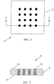
- FIGS. 1 and 2 depict a preferred feedthrough assembly 8 in accordance with the present disclosure comprising a thin ceramic sheet 10 of ceramic material having multiple electrical feedthroughs 12 extending therethrough terminating flush with the upper and lower surfaces 14 , 16 of sheet 10.
- the sheet 10 typically comprises a wall portion of a housing (not shown) for accommodating electronic circuitry.
- the feedthroughs 12 function to electrically connect devices external to the housing, e.g., adjacent to surface 14, to electronic circuitry contained within the housing, e.g., adjacent to surface 16.
- "Thin ceramic sheet” as used herein refers to a sheet having a finished thickness dimension of ⁇ 40 mils, i.e., 1 mm.
- the apparatus in accordance with the disclosure is particularly suited for use in corrosive environments such as in medical devices implanted in a patient's body.
- the present disclosure is directed to providing electrical feedthroughs that are compatible with thin ceramic sheets (or substrates) having a finished thickness of ⁇ 1 mm ( ⁇ 40 mils), and with feedthroughs that are hermetic, biocompatible, and electrochemically stable.
- the ceramic sheet 10 may be formed of 90% aluminum oxide (AlO 2 ) and the feedthroughs 12 may have a diameter of ⁇ 0.5 mm ( ⁇ 20 mils) and may be composed of paste containing, for example, platinum.
- FIGS. 3 and 4A -4M depict the possible process steps for fabricating the finished feedthrough assembly 8 illustrated in FIGS. 1 and 2 .
- a green ceramic sheet/tape/substrate 20 ( FIG. 4A ), formed, for example, of >90% aluminum oxide (AlO 2 ) is selected as represented by step 21 in FIG. 3 .
- the sheet 20 may have a thickness of 1 mm (40 mils) or less.
- Green ceramic sheet/tape/substrate refers to an unfired ceramic sheet, tape or substrate.
- Via holes 26 are formed into the sheet 20 as represented by FIGs. 4B-4C and step 28 in FIG. 3 .
- each via hole 26 may be punched in to the sheet 20 using, for example, programmable punch tool 27.
- a plurality of via holes 26 may be punched at the same time. It is to be understood that other methods may be used to form via holes 26.
- via holes 26 may be formed using solvent etching, laser ablation, and/or via holes 26 may be drilled.
- Step 37 of FIG. 3 calls for selecting a conductive thickfilm paste 17 to fill in via holes 26 depicted in FIG. 4C .
- Thiickfilm paste refers to a material containing inorganic particles dispersed in a vehicle comprising an organic resin and a solvent. Types of different pastes are disclosed in US Patent No. 5601638 .
- a stencil printing with vacuum pull down process may be used to fill via holes 26 with the conductive paste 17 as represented by FIGs. 4D-4E and step 39 in FIG. 3 .
- the sheet 20 may sandwiched between a stencil layer 19 and a vacuum base 80.
- a vacuum chuck 81 of the vacuum base 80 pulls the conductive paste 17 through holes 82 of the stencil layer 19 and into the via holes 26 as shown in FIGs. 4D-4E .
- Step 40 of FIG. 3 calls for determining if additional green ceramic sheet/tape/substrates with paste filled via holes are required. If additional green ceramic sheet/tape/substrates with paste filled via holes are required ("Yes” in step 40), steps 21 , 28 , 37 and 39 are repeated. If additional green ceramic sheet/tape/substrates with paste filled via holes are not required ("No” in step 40 ), step 41 of FIG. 3 is performed.
- the sheet 20 with via holes 26 filled with conductive paste 17 shown in figure FIG. 4F may go through a multilayer lamination process as represented by FIGs. 4G-4H and step 41 in FIG. 3 .
- the sheet 20 of FIG. 4F may be laminated with, for example, sheets 91 and 92 as shown in FIG. 4G .
- the sheets 91 and 92 may contain conductive paste filled vias 26 that are similar to the conductive paste filled vias 26 of the sheet 20 and the sheets 91 and 92 may be formed using steps 21, 28, 37 and 39 of FIG. 3 as described above.
- the sheets 20 , 91 and 92 are stacked on top of each other with conductive paste filled vias 26 of each sheet being aligned on top of each other; b) stacked sheets 20 , 91 and 92 are sandwiched between two unpunched green ceramic sheets/tapes/substrates 95 and 96 ; and c) the sheets 20 , 91 and 92 and the sheets 95 and 96 are laminated together using a heatpress 98 to create laminated substrate 100 shown in FIG. 4I .
- FIGs. 4G and 4H laminate three sheets 20, 91 and 92 with conductive paste filled vias 26, one skilled in the art can appreciate that this disclosure is not limited to three sheets and that a single sheet 20 with conductive paste filled vias may be laminated together with the sheets 95 and 96 without the additional sheets 91 and 92.
- FIGs. 4G and 4H laminate three sheets 20 , 91 and 92 with conductive paste filled vias 26 , one skilled in the art can appreciate that this disclosure is not limited to three sheets and that additional sheets with conductive paste filled vias may also be laminated together with sheets 20 , 91 and 92.
- Step 44 of FIG. 3 calls for the laminated substrate 100 to be fired. Firing of the laminated substrate 100 encompasses different aspects of forming bonds in ceramic (evaporation, binder burnout, sintering, etc.).
- the unpunched ceramic layers 95 and 96 of the laminated substrate 100 help to constrain the conductive paste within via holes 26 and allow for compression during the firing step 44.
- the unpunched ceramic layers 95 and 96 of the laminated substrate 100 also help to isolate the conductive paste filled vias 26 from the firing atmosphere during the step 44 which may be the key to hermetic and low resistance paste filled vias 26.
- An exemplary firing schedule includes ramping the laminated substrate 100 of FIG. 4I up to 600°C at a rate of 1°C/minute, then ramping up to 1600°C at a rate at 5°C/minute, followed by a one hour dwell and then a cool-to-room-temperature interval.
- the ceramic material of the laminated substrate 100 shrinks thereby shrinking via holes 26 around the paste 17 to form a seal.
- the fine aluminum oxide suspension permits uniform and continuous sealing around the surface of the paste 17.
- the paste 17 being squeezed by the ceramic exhibits sufficient flow to enable the paste 17 to flow and fill any crevices in the ceramic. This action produces a hermetic paste/ceramic interface.
- the firing step 44 may also cause hermeticity through bonding mechanisms like, for example, sintering, glass melt/wetting, alloying, compounding and/or diffusion solution formation. "Sintering" as used herein is a term used to describe the consolidation of the ceramic material during firing.
- Compounding refers to a chemical compound that is a substance consisting of two or more elements chemically-bonded together in a fixed proportion by mass.
- “Diffusion solution formation” as used herein refers is the net movement of particles from an area of high concentration to an area of low concentration.
- a solid solution is a solid-state solution of one or more solutes in a solvent. Such a mixture is considered a solution rather than a compound when the crystal structure of the solvent remains unchanged by addition of the solutes, and when the mixture remains in a single homogeneous phase.
- the firing step 44 may also cause solidification of the metalized vias 26 and the ceramic material of the laminated substrate 100 to prevent leaks.
- Step 48 of FIG. 3 calls for lapping or grinding the upper and lower surfaces of the fired laminated substrate 100 to remove materials 50 and 51 , depicted in FIG. 4J , in order to expose the upper and lower faces of the metalized vias 26.
- the upper and lower surfaces of the fired laminated substrate 100 may also go through the polishing step 49 so that the metalized vias 26 are flush with the surrounding ceramic material.
- the fired laminated substrate 100 may be subjected to a hermeticity test, e.g., frequently a helium (He) leak test as represented by step 56 in FIG. 3 .
- a hermeticity test e.g., frequently a helium (He) leak test as represented by step 56 in FIG. 3 .
- He helium
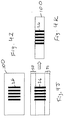
- sheet/substrate 20 may contain several patterns 24a-d of the via holes 26 as shown in Fig. 4L .
- the fired laminated substrate 100 would contain several patterns 24a-d of the metal filled via holes 26 and the fired laminated substrate 100 would be subjected to a singulation or dicing step 58 to provide multiple feedthrough assemblies 60A, 60B, 60C, 60D shown in FIG. 4M .
- the conductive paste 17 may comprise any of the noble metals and/or any of the refractory metals, for example, platinum, titanium, gold, palladum, tantalum, niobium.
Landscapes
- Engineering & Computer Science (AREA)
- Manufacturing & Machinery (AREA)
- Microelectronics & Electronic Packaging (AREA)
- Chemical & Material Sciences (AREA)
- Ceramic Engineering (AREA)
- Materials Engineering (AREA)
- Structural Engineering (AREA)
- Organic Chemistry (AREA)
- Inorganic Chemistry (AREA)
- Printing Elements For Providing Electric Connections Between Printed Circuits (AREA)
- Ceramic Products (AREA)
- Production Of Multi-Layered Print Wiring Board (AREA)
- Prostheses (AREA)
Claims (19)
- Procédé de fabrication d'une traversée électrique hermétique (12), le procédé comprenant :la fourniture d'une feuille de céramique (20) ayant une surface supérieure et une surface inférieure ;la formation d'au moins un trou d'interconnexion (26) dans ladite feuille de céramique (20) s'étendant de ladite surface supérieure à ladite surface inférieure ;l'insertion d'une pâte conductrice en couche épaisse (17) dans ledit trou d'interconnexion (26), la pâte en couche épaisse comprenant un métal choisi dans le groupe constitué de : platine, titane, or, palladium, tantale et niobium ;la stratification de la feuille de céramique (20) avec le trou d'interconnexion (26) rempli de pâte entre une feuille de céramique supérieure (95) et une feuille de céramique inférieure (96) pour former un substrat de céramique stratifié (100) ;la cuisson du substrat de céramique stratifié (100) à une température pour fritter le substrat de céramique stratifié et amener le trou d'interconnexion rempli de pâte (26) à former un trou métallisé et amener le substrat de céramique stratifié (100) à former un joint hermétique autour dudit trou métallisé (26) ; etcaractérisé en ce que :
le procédé inclut en outre l'étape de retrait du matériau de la feuille de céramique supérieure (95, 50) et de la feuille de céramique inférieure (96, 51) du substrat de céramique stratifié (100) cuit pour exposer une surface supérieure et une surface inférieure du trou métallisé (26). - Procédé selon la revendication 1, dans lequel ladite feuille de céramique (20) est formée de matériau composé d'au moins 90 % d'oxyde d'aluminium.
- Procédé selon la revendication 1 ou 2, dans lequel ladite feuille de céramique (20) est formée de matériau composé d'au moins 92 % d'oxyde d'aluminium.
- Procédé selon l'une quelconque des revendications précédentes, dans lequel ladite feuille de céramique (20) après lesdites étapes de cuisson et de retrait de matériau est inférieure ou égale à 1 mm (40 mils) d'épaisseur.
- Procédé selon l'une quelconque des revendications précédentes, dans lequel ladite feuille de céramique (20) après lesdites étapes de cuisson et de retrait de matériau est inférieure à 0,4 mm (15 mils) d'épaisseur.
- Procédé selon l'une quelconque des revendications précédentes, dans lequel ladite pâte (17) comprend du platine.
- Procédé selon l'une quelconque des revendications précédentes, dans lequel le trou métallisé (26) a un diamètre inférieur ou égal à 0,5 mm (20 mils).
- Procédé selon l'une quelconque des revendications précédentes, dans lequel le trou métallisé (26) a un diamètre inférieur ou égal à 0,25 mm (10 mils).
- Procédé selon l'une quelconque des revendications précédentes, dans lequel la feuille de céramique (20) est non cuite.
- Procédé selon l'une quelconque des revendications précédentes, dans lequel la formation d'au moins un trou d'interconnexion (26) dans ladite feuille de céramique (20) comprend la perforation du trou d'interconnexion (26) au moyen d'un outil de perforation (27), la gravure du trou d'interconnexion (26) au moyen d'une gravure par solvant, au moyen d'une ablation au laser ou d'un perçage du trou d'interconnexion (26).
- Procédé selon l'une quelconque des revendications précédentes, dans lequel l'insertion d'une pâte conductrice en couche épaisse (17) dans ledit trou d'interconnexion (26) comprend :la disposition de la feuille de céramique (20) avec le trou d'interconnexion (26) entre une couche pochoir (19) et une base de vide (80), dans lequel la couche pochoir (19) inclut au moins un trou traversant (82) qui est aligné au-dessus du trou d'interconnexion (26) ;l'enroulement de la pâte conductrice en couche épaisse (17) sur la couche pochoir (19); etla traction de la pâte conductrice en couche épaisse (17) dans le trou d'interconnexion (26) à travers le trou (82) dans la couche pochoir (19) avec un vide créé par la base de vide (80).
- Procédé selon l'une quelconque des revendications précédentes, dans lequel la stratification de la feuille de céramique (20) avec les trous d'interconnexion remplis de pâte (26) entre la feuille de céramique supérieure (95) et la feuille de céramique inférieure (96) pour former le substrat de céramique stratifié (100) comprend :la mise en place de la feuille de céramique (20) avec les trous d'interconnexion remplis de pâte (26) conjointement avec la feuille de céramique supérieure (95) et la feuille de céramique inférieure (96) dans une presse chauffante (98) ; etl'application de chaleur et de pression au moyen de la presse chauffante (98) jusqu'à ce que le substrat de céramique stratifié (100) soit formé.
- Procédé selon l'une quelconque des revendications précédentes, dans lequel la cuisson du substrat de céramique stratifié (100) comprend l'évaporation, le brûlage du liant et le frittage du substrat de céramique stratifié (100).
- Procédé selon l'une quelconque des revendications, dans lequel ledit matériau de céramique (20) comprend de l'oxyde d'aluminium, de l'oxyde de zirconium ou un mélange de ceux-ci.
- Procédé selon l'une quelconque des revendications précédentes, dans lequel ledit matériau de céramique (20) comprend moins de 99 % d'oxyde d'aluminium.
- Procédé selon l'une quelconque des revendications précédentes, dans lequel le substrat de céramique stratifié (100) cuit a une épaisseur de moins de 0,5 mm (20 mils) après retrait du matériau de la feuille de céramique supérieure (95, 50) et de la feuille de céramique inférieure (96, 51).
- Procédé selon l'une quelconque des revendications précédentes, dans lequel le substrat de céramique stratifié (100) cuit a une épaisseur de 0,4 à 0,5 mm (15 à 20 mils) après retrait du matériau de la couche de céramique supérieure (95, 50) et de la couche de céramique inférieure (96, 51).
- Procédé selon l'une quelconque des revendications précédentes, dans lequel ladite pâte conductrice en couche épaisse (17) comprend un métal noble, un métal réfractaire ou un mélange de ceux-ci.
- Procédé selon la revendication 1, dans lequel :l'étape de fourniture d'une feuille de céramique (20) comprend la fourniture d'une pluralité de feuilles de céramique (20, 91, 92) ayant une surface supérieure et une surface inférieure ;l'étape de formation d'au moins un trou d'interconnexion (26) comprend la formation d'une pluralité de trous d'interconnexion (26) dans chacune des feuilles de céramique s'étendant de ladite surface supérieure à ladite surface inférieure de chaque feuille de céramique (20, 91, 92) ;l'étape d'insertion d'une pâte conductrice (17) comprend l'insertion d'une pâte conductrice en couche épaisse (17) dans les trous d'interconnexion (26) de chaque feuille de céramique (20, 91, 92) ; etl'étape de stratification de la feuille de céramique (20, 91, 92) comprend l'empilement de la pluralité de feuilles de céramique (20, 91, 92) les unes au-dessus des autres, dans lequel les trous d'interconnexion (26) remplis avec de la pâte conductrice en couche épaisse (17) de chaque feuille de céramique (20, 91, 92) sont sensiblement alignés avec les trous d'interconnexion (26) remplis avec de la pâte conductrice en couche épaisse (17) des autres feuilles de céramique (20, 91, 92), prenant en sandwich les feuilles de céramique (20, 91, 92) empilées entre une feuille de céramique supérieure (95) et une feuille de céramique inférieure (96), et stratifiant la pluralité de feuilles de céramique (20, 91, 92) empilées avec la feuille de céramique inférieure (96) et la feuille de céramique supérieure (95) pour former le substrat de céramique stratifié (100).
Applications Claiming Priority (2)
| Application Number | Priority Date | Filing Date | Title |
|---|---|---|---|
| US94608607P | 2007-06-25 | 2007-06-25 | |
| PCT/US2007/081947 WO2009002355A1 (fr) | 2007-06-25 | 2007-10-19 | Procédé permettant de fournir une traversée électrique hermétique |
Publications (2)
| Publication Number | Publication Date |
|---|---|
| EP2174535A1 EP2174535A1 (fr) | 2010-04-14 |
| EP2174535B1 true EP2174535B1 (fr) | 2019-12-04 |
Family
ID=39577709
Family Applications (1)
| Application Number | Title | Priority Date | Filing Date |
|---|---|---|---|
| EP07871188.4A Active EP2174535B1 (fr) | 2007-06-25 | 2007-10-19 | Procédé permettant de fournir une traversée électrique hermétique |
Country Status (4)
| Country | Link |
|---|---|
| US (4) | US20080314502A1 (fr) |
| EP (1) | EP2174535B1 (fr) |
| AU (1) | AU2007355605B2 (fr) |
| WO (1) | WO2009002355A1 (fr) |
Families Citing this family (36)
| Publication number | Priority date | Publication date | Assignee | Title |
|---|---|---|---|---|
| DE102006041940A1 (de) * | 2006-09-07 | 2008-03-27 | Biotronik Crm Patent Ag | Elektrische Durchführung |
| EP2174535B1 (fr) * | 2007-06-25 | 2019-12-04 | Second Sight Medical Products, Inc. | Procédé permettant de fournir une traversée électrique hermétique |
| DE102008004308A1 (de) * | 2008-01-15 | 2009-07-16 | Biotronik Crm Patent Ag | Durchführung für eine Batterie, Verfahren zur Herstellung derselben und Batterie |
| US10390441B1 (en) | 2008-05-28 | 2019-08-20 | Second Sight Medical Products, Inc. | Method for providing hermetic electrical feedthrough |
| US8698006B2 (en) | 2009-06-04 | 2014-04-15 | Morgan Advanced Ceramics, Inc. | Co-fired metal and ceramic composite feedthrough assemblies for use at least in implantable medical devices and methods for making the same |
| US8563113B2 (en) * | 2010-04-20 | 2013-10-22 | Corning Incorporated | Multi-laminate hermetic barriers and related structures and methods of hermetic sealing |
| DE102011009858B8 (de) | 2011-01-31 | 2013-11-07 | Heraeus Precious Metals Gmbh & Co. Kg | Cermethaltige Durchführung für eine medizinisch inplantierbare Vorrichtung mit Verbindungsschicht |
| DE102011009855B8 (de) | 2011-01-31 | 2013-01-03 | Heraeus Precious Metals Gmbh & Co. Kg | Keramikdurchführung mit induktivem Filter |
| DE102011009867B4 (de) | 2011-01-31 | 2013-09-05 | Heraeus Precious Metals Gmbh & Co. Kg | Keramikdurchführung für eine medizinisch implantierbare Vorrichtung |
| US11198014B2 (en) | 2011-03-01 | 2021-12-14 | Greatbatch Ltd. | Hermetically sealed filtered feedthrough assembly having a capacitor with an oxide resistant electrical connection to an active implantable medical device housing |
| US10596369B2 (en) | 2011-03-01 | 2020-03-24 | Greatbatch Ltd. | Low equivalent series resistance RF filter for an active implantable medical device |
| WO2012158845A2 (fr) * | 2011-05-16 | 2012-11-22 | Lawrence Livermore National Security, Llc | Procédé de fabrication de connexions d'interface électriques hermétiques à haute densité au moyen de faisceaux de câbles isolés |
| US9627833B2 (en) | 2011-08-02 | 2017-04-18 | Medtronic, Inc. | Electrical leads for a feedthrough |
| US8841558B2 (en) | 2011-08-02 | 2014-09-23 | Medtronic Inc. | Hermetic feedthrough |
| US8588916B2 (en) | 2011-08-02 | 2013-11-19 | Medtronic, Inc. | Feedthrough configured for interconnect |
| US9724524B2 (en) | 2011-08-02 | 2017-08-08 | Medtronic, Inc. | Interconnection of conductor to feedthrough |
| US8872035B2 (en) | 2011-08-02 | 2014-10-28 | Medtronic, Inc. | Hermetic feedthrough |
| US8670829B2 (en) | 2011-08-02 | 2014-03-11 | Medtronic, Inc. | Insulator for a feedthrough |
| US9008779B2 (en) | 2011-08-02 | 2015-04-14 | Medtronic, Inc. | Insulator for a feedthrough |
| EP3366348B1 (fr) | 2012-01-16 | 2023-08-23 | Greatbatch Ltd. | Traversée hermétique co-connectée filtrée emi, condensateur de traversée et ensemble de dérivation pour dispositif médical implantable actif |
| US10881867B2 (en) | 2012-01-16 | 2021-01-05 | Greatbatch Ltd. | Method for providing a hermetically sealed feedthrough with co-fired filled via for an active implantable medical device |
| US10420949B2 (en) * | 2012-01-16 | 2019-09-24 | Greatbatch Ltd. | Method of manufacturing a feedthrough insulator for an active implantable medical device incorporating a post conductive paste filled pressing step |
| US10046166B2 (en) | 2012-01-16 | 2018-08-14 | Greatbatch Ltd. | EMI filtered co-connected hermetic feedthrough, feedthrough capacitor and leadwire assembly for an active implantable medical device |
| US9889306B2 (en) | 2012-01-16 | 2018-02-13 | Greatbatch Ltd. | Hermetically sealed feedthrough with co-fired filled via and conductive insert for an active implantable medical device |
| WO2014049089A1 (fr) * | 2012-09-28 | 2014-04-03 | Csem Centre Suisse D'electronique Et De Microtechnique Sa - Recherche Et Developpement | Dispositifs implantables |
| USRE46699E1 (en) | 2013-01-16 | 2018-02-06 | Greatbatch Ltd. | Low impedance oxide resistant grounded capacitor for an AIMD |
| US9591770B2 (en) | 2013-04-26 | 2017-03-07 | Kla-Tencor Corporation | Multi-layer ceramic vacuum to atmosphere electric feed through |
| US9892816B2 (en) * | 2013-06-27 | 2018-02-13 | Heraeus Precious Metals North America Conshohocken Llc | Platinum containing conductive paste |
| CN107207367A (zh) * | 2014-05-07 | 2017-09-26 | 摩根先进陶瓷公司 | 用于制造大型共烧物件的改进的方法 |
| WO2018058181A1 (fr) * | 2016-09-30 | 2018-04-05 | Dyesol Ltd | Module solaire et procédé de fabrication d'un module solaire |
| US10249415B2 (en) | 2017-01-06 | 2019-04-02 | Greatbatch Ltd. | Process for manufacturing a leadless feedthrough for an active implantable medical device |
| CN111373487B (zh) * | 2017-10-24 | 2024-09-24 | 沃特洛电气制造公司 | 设有陶瓷绝缘体和铝套的电连接器及其制造方法 |
| CN108276019B (zh) * | 2018-03-01 | 2020-10-27 | 清华大学 | 精密真空转子球腔装置及其陶瓷电极引针的封接方法 |
| KR20220035406A (ko) | 2019-07-12 | 2022-03-22 | 뉴럴링크 코포레이션 | 밀폐 밀봉된 전자 장치를 위한 단일체의 생체적합성 피드스루 및 그 제조 방법들 |
| CN110304935B (zh) * | 2019-08-08 | 2021-11-26 | 贵州大学 | 一种陶瓷微通道的封装方法 |
| EP4147746A1 (fr) | 2021-09-10 | 2023-03-15 | Greatbatch Ltd. | Composite métallique renforcé céramique pour corps hermétiques pour dispositifs implantables |
Citations (5)
| Publication number | Priority date | Publication date | Assignee | Title |
|---|---|---|---|---|
| US5604018A (en) * | 1993-06-25 | 1997-02-18 | Shinko Electric Industries, Co., Ltd. | Ceramic oxide circuit board |
| US5855711A (en) * | 1996-03-28 | 1999-01-05 | Sumitomo Metal (Smi) Electronics Devices Inc. | Method of producing a ceramic circuit substrate |
| US6284080B1 (en) * | 1997-02-21 | 2001-09-04 | Medtronic, Inc. | Barrier metallization in ceramic substrate for implantable medical devices |
| WO2002078781A2 (fr) * | 2001-03-30 | 2002-10-10 | Second Sight, Llc | Dispositif et procede permettant de former une traversee electrique hermetique |
| US6660116B2 (en) * | 2000-03-01 | 2003-12-09 | Medtronic, Inc. | Capacitive filtered feedthrough array for an implantable medical device |
Family Cites Families (36)
| Publication number | Priority date | Publication date | Assignee | Title |
|---|---|---|---|---|
| GB1319774A (en) * | 1969-06-26 | 1973-06-06 | Nat Res Dev | Visual prosthetic device |
| US4526535A (en) * | 1983-12-27 | 1985-07-02 | The Maytag Company | Gas burner for a combined laundry appliance |
| US4573481A (en) * | 1984-06-25 | 1986-03-04 | Huntington Institute Of Applied Research | Implantable electrode array |
| US4628933A (en) | 1985-07-23 | 1986-12-16 | Michelson Robin P | Method and apparatus for visual prosthesis |
| US5006286A (en) * | 1986-03-31 | 1991-04-09 | Amp Incorporated | Polymeric electrical interconnection apparatus and method of use |
| US4837049A (en) * | 1986-06-17 | 1989-06-06 | Alfred E. Mann Foundation For Scientific Research | Method of making an electrode array |
| WO1988005959A1 (fr) * | 1987-02-04 | 1988-08-11 | Coors Porcelain Company | Substrat ceramique presentant des passages remplis d'une substance conductrice et procede de production |
| JP2765885B2 (ja) * | 1988-11-14 | 1998-06-18 | 新光電気工業株式会社 | 窒化アルミニウム回路基板及びその製造方法 |
| US5215088A (en) * | 1989-11-07 | 1993-06-01 | The University Of Utah | Three-dimensional electrode device |
| US5611140A (en) * | 1989-12-18 | 1997-03-18 | Epoxy Technology, Inc. | Method of forming electrically conductive polymer interconnects on electrical substrates |
| US5085720A (en) * | 1990-01-18 | 1992-02-04 | E. I. Du Pont De Nemours And Company | Method for reducing shrinkage during firing of green ceramic bodies |
| US5109844A (en) * | 1990-10-11 | 1992-05-05 | Duke University | Retinal microstimulation |
| US5216207A (en) * | 1991-02-27 | 1993-06-01 | David Sarnoff Research Center, Inc. | Low temperature co-fired multilayer ceramic circuit boards with silver conductors |
| US5283104A (en) * | 1991-03-20 | 1994-02-01 | International Business Machines Corporation | Via paste compositions and use thereof to form conductive vias in circuitized ceramic substrates |
| US5302219A (en) * | 1991-04-03 | 1994-04-12 | Coors Electronic Package Company | Method for obtaining via patterns in ceramic sheets |
| JP3166251B2 (ja) * | 1991-12-18 | 2001-05-14 | 株式会社村田製作所 | セラミック多層電子部品の製造方法 |
| US5340947A (en) * | 1992-06-22 | 1994-08-23 | Cirqon Technologies Corporation | Ceramic substrates with highly conductive metal vias |
| US5470412A (en) * | 1992-07-30 | 1995-11-28 | Sumitomo Metal Ceramics Inc. | Process for producing a circuit substrate |
| CA2105448A1 (fr) * | 1992-09-05 | 1994-03-06 | Michio Horiuchi | Carte a circuits imprimees en nitrure d'aluminium et methode de fabrication |
| US5468936A (en) * | 1993-03-23 | 1995-11-21 | Philip Morris Incorporated | Heater having a multiple-layer ceramic substrate and method of fabrication |
| DE19707046A1 (de) * | 1997-02-21 | 1998-08-27 | Rolf Prof Dr Ing Eckmiller | Lernfähiger "Active Vision" Implant Encoder |
| US6458157B1 (en) * | 1997-08-04 | 2002-10-01 | Suaning Gregg Joergen | Retinal stimulator |
| US6194053B1 (en) * | 1998-02-26 | 2001-02-27 | International Business Machines Corporation | Apparatus and method fabricating buried and flat metal features |
| US5935155A (en) * | 1998-03-13 | 1999-08-10 | John Hopkins University, School Of Medicine | Visual prosthesis and method of using same |
| US6205032B1 (en) * | 1999-03-16 | 2001-03-20 | Cts Corporation | Low temperature co-fired ceramic with improved registration |
| JP2000290077A (ja) * | 1999-04-09 | 2000-10-17 | Matsushita Electric Ind Co Ltd | 積層セラミック電子部品の製造方法 |
| US6139666A (en) * | 1999-05-26 | 2000-10-31 | International Business Machines Corporation | Method for producing ceramic surfaces with easily removable contact sheets |
| US6361716B1 (en) * | 2000-07-20 | 2002-03-26 | Dow Corning Corporation | Silicone composition and electrically conductive silicone adhesive formed therefrom |
| US6743534B2 (en) * | 2001-10-01 | 2004-06-01 | Heraeus Incorporated | Self-constrained low temperature glass-ceramic unfired tape for microelectronics and methods for making and using the same |
| DE102004043273A1 (de) * | 2003-09-09 | 2005-05-04 | Ngk Spark Plug Co | Verfahren zur Herstellung eines Keramiksubstrats und Keramiksubstrat |
| JPWO2005039263A1 (ja) * | 2003-10-17 | 2007-02-15 | 日立金属株式会社 | 多層セラミック基板及びその製造方法並びにこれを用いた電子機器 |
| JP4297163B2 (ja) * | 2004-10-08 | 2009-07-15 | パナソニック株式会社 | 多層回路基板の製造方法 |
| US20060162844A1 (en) * | 2005-01-26 | 2006-07-27 | Needes Christopher R | Multi-component LTCC substrate with a core of high dielectric constant ceramic material and processes for the development thereof |
| EP1879649B1 (fr) * | 2005-04-28 | 2013-05-15 | Second Sight Medical Products, Inc. | Boitier conçu pour un dispositif de stimulation neuronale implantable |
| US7164572B1 (en) * | 2005-09-15 | 2007-01-16 | Medtronic, Inc. | Multi-path, mono-polar co-fired hermetic electrical feedthroughs and methods of fabrication therfor |
| EP2174535B1 (fr) * | 2007-06-25 | 2019-12-04 | Second Sight Medical Products, Inc. | Procédé permettant de fournir une traversée électrique hermétique |
-
2007
- 2007-10-19 EP EP07871188.4A patent/EP2174535B1/fr active Active
- 2007-10-19 AU AU2007355605A patent/AU2007355605B2/en not_active Ceased
- 2007-10-19 US US11/875,198 patent/US20080314502A1/en not_active Abandoned
- 2007-10-19 WO PCT/US2007/081947 patent/WO2009002355A1/fr not_active Ceased
- 2007-10-25 US US11/924,408 patent/US8551271B2/en active Active
-
2013
- 2013-11-14 US US14/080,549 patent/US9717150B2/en active Active
-
2017
- 2017-06-19 US US15/626,437 patent/US9936590B2/en active Active
Patent Citations (5)
| Publication number | Priority date | Publication date | Assignee | Title |
|---|---|---|---|---|
| US5604018A (en) * | 1993-06-25 | 1997-02-18 | Shinko Electric Industries, Co., Ltd. | Ceramic oxide circuit board |
| US5855711A (en) * | 1996-03-28 | 1999-01-05 | Sumitomo Metal (Smi) Electronics Devices Inc. | Method of producing a ceramic circuit substrate |
| US6284080B1 (en) * | 1997-02-21 | 2001-09-04 | Medtronic, Inc. | Barrier metallization in ceramic substrate for implantable medical devices |
| US6660116B2 (en) * | 2000-03-01 | 2003-12-09 | Medtronic, Inc. | Capacitive filtered feedthrough array for an implantable medical device |
| WO2002078781A2 (fr) * | 2001-03-30 | 2002-10-10 | Second Sight, Llc | Dispositif et procede permettant de former une traversee electrique hermetique |
Also Published As
| Publication number | Publication date |
|---|---|
| US20080314502A1 (en) | 2008-12-25 |
| US8551271B2 (en) | 2013-10-08 |
| US20170290171A1 (en) | 2017-10-05 |
| EP2174535A1 (fr) | 2010-04-14 |
| US20140076844A1 (en) | 2014-03-20 |
| US20080314865A1 (en) | 2008-12-25 |
| WO2009002355A1 (fr) | 2008-12-31 |
| AU2007355605B2 (en) | 2012-04-26 |
| AU2007355605A1 (en) | 2008-12-31 |
| US9936590B2 (en) | 2018-04-03 |
| US9717150B2 (en) | 2017-07-25 |
Similar Documents
| Publication | Publication Date | Title |
|---|---|---|
| EP2174535B1 (fr) | Procédé permettant de fournir une traversée électrique hermétique | |
| EP1934994B1 (fr) | Trous d'interconnexion electriques, cofrittes, implantables | |
| US7901761B1 (en) | Hermetic vias utilizing metal-metal oxides | |
| US7480988B2 (en) | Method and apparatus for providing hermetic electrical feedthrough | |
| US9782111B2 (en) | Hermetic feedthrough assembly for ceramic body | |
| US20070060970A1 (en) | Miniaturized co-fired electrical interconnects for implantable medical devices | |
| US20110000699A1 (en) | Co-fired metal and ceramic composite feedthrough assemblies for use at least in implantable medical devices and methods for making the same | |
| CN109574637B (zh) | 带馈通电极的陶瓷基板及其制造方法 | |
| JP2010087266A (ja) | 複合基板及びその製造方法 | |
| CN109315070A (zh) | 多层基板的制造方法 | |
| US10952332B2 (en) | Method for providing hermetic electrical feedthrough | |
| CN1006440B (zh) | 混合与多层电路 | |
| JP3112258B2 (ja) | 回路基板とその製造方法 | |
| WO2008075504A1 (fr) | Procédé de fabrication d'un condensateur à couche mince, condensateur à couche mince et procédé de fabrication d'une carte de câblage avec un condensateur incorporé | |
| JP4735018B2 (ja) | 多層セラミック基板およびその製造方法 | |
| JP2003347160A (ja) | 多連型コンデンサ | |
| JP2812605B2 (ja) | 多層セラミック基板の製造方法 | |
| JP4413223B2 (ja) | セラミックパッケージ | |
| JP4735016B2 (ja) | 多層セラミック基板およびその製造方法 | |
| JP4413224B2 (ja) | セラミックパッケージ | |
| JPH10135636A (ja) | セラミック多層基板およびその製造方法 |
Legal Events
| Date | Code | Title | Description |
|---|---|---|---|
| PUAI | Public reference made under article 153(3) epc to a published international application that has entered the european phase |
Free format text: ORIGINAL CODE: 0009012 |
|
| 17P | Request for examination filed |
Effective date: 20100122 |
|
| AK | Designated contracting states |
Kind code of ref document: A1 Designated state(s): AT BE BG CH CY CZ DE DK EE ES FI FR GB GR HU IE IS IT LI LT LU LV MC MT NL PL PT RO SE SI SK TR |
|
| AX | Request for extension of the european patent |
Extension state: AL BA HR MK RS |
|
| DAX | Request for extension of the european patent (deleted) | ||
| 17Q | First examination report despatched |
Effective date: 20120518 |
|
| TPAC | Observations filed by third parties |
Free format text: ORIGINAL CODE: EPIDOSNTIPA |
|
| STAA | Information on the status of an ep patent application or granted ep patent |
Free format text: STATUS: EXAMINATION IS IN PROGRESS |
|
| TPAC | Observations filed by third parties |
Free format text: ORIGINAL CODE: EPIDOSNTIPA |
|
| REG | Reference to a national code |
Ref country code: DE Ref legal event code: R079 Ref document number: 602007059587 Country of ref document: DE Free format text: PREVIOUS MAIN CLASS: H05K0003400000 Ipc: B32B0037140000 |
|
| GRAP | Despatch of communication of intention to grant a patent |
Free format text: ORIGINAL CODE: EPIDOSNIGR1 |
|
| STAA | Information on the status of an ep patent application or granted ep patent |
Free format text: STATUS: GRANT OF PATENT IS INTENDED |
|
| RIC1 | Information provided on ipc code assigned before grant |
Ipc: H05K 3/00 20060101ALI20180713BHEP Ipc: H05K 3/12 20060101ALI20180713BHEP Ipc: H05K 3/46 20060101ALI20180713BHEP Ipc: H05K 1/03 20060101ALI20180713BHEP Ipc: H05K 3/40 20060101ALI20180713BHEP Ipc: C04B 37/00 20060101ALI20180713BHEP Ipc: B32B 37/14 20060101AFI20180713BHEP Ipc: C04B 35/10 20060101ALI20180713BHEP |
|
| INTG | Intention to grant announced |
Effective date: 20180802 |
|
| RAP1 | Party data changed (applicant data changed or rights of an application transferred) |
Owner name: SECOND SIGHT MEDICAL PRODUCTS, INC. |
|
| GRAJ | Information related to disapproval of communication of intention to grant by the applicant or resumption of examination proceedings by the epo deleted |
Free format text: ORIGINAL CODE: EPIDOSDIGR1 |
|
| STAA | Information on the status of an ep patent application or granted ep patent |
Free format text: STATUS: EXAMINATION IS IN PROGRESS |
|
| INTC | Intention to grant announced (deleted) | ||
| GRAP | Despatch of communication of intention to grant a patent |
Free format text: ORIGINAL CODE: EPIDOSNIGR1 |
|
| STAA | Information on the status of an ep patent application or granted ep patent |
Free format text: STATUS: GRANT OF PATENT IS INTENDED |
|
| INTG | Intention to grant announced |
Effective date: 20190618 |
|
| GRAS | Grant fee paid |
Free format text: ORIGINAL CODE: EPIDOSNIGR3 |
|
| GRAA | (expected) grant |
Free format text: ORIGINAL CODE: 0009210 |
|
| STAA | Information on the status of an ep patent application or granted ep patent |
Free format text: STATUS: THE PATENT HAS BEEN GRANTED |
|
| AK | Designated contracting states |
Kind code of ref document: B1 Designated state(s): AT BE BG CH CY CZ DE DK EE ES FI FR GB GR HU IE IS IT LI LT LU LV MC MT NL PL PT RO SE SI SK TR |
|
| REG | Reference to a national code |
Ref country code: GB Ref legal event code: FG4D |
|
| REG | Reference to a national code |
Ref country code: CH Ref legal event code: EP |
|
| REG | Reference to a national code |
Ref country code: AT Ref legal event code: REF Ref document number: 1208880 Country of ref document: AT Kind code of ref document: T Effective date: 20191215 |
|
| REG | Reference to a national code |
Ref country code: DE Ref legal event code: R096 Ref document number: 602007059587 Country of ref document: DE |
|
| REG | Reference to a national code |
Ref country code: IE Ref legal event code: FG4D |
|
| REG | Reference to a national code |
Ref country code: NL Ref legal event code: MP Effective date: 20191204 |
|
| REG | Reference to a national code |
Ref country code: LT Ref legal event code: MG4D |
|
| PG25 | Lapsed in a contracting state [announced via postgrant information from national office to epo] |
Ref country code: ES Free format text: LAPSE BECAUSE OF FAILURE TO SUBMIT A TRANSLATION OF THE DESCRIPTION OR TO PAY THE FEE WITHIN THE PRESCRIBED TIME-LIMIT Effective date: 20191204 Ref country code: LT Free format text: LAPSE BECAUSE OF FAILURE TO SUBMIT A TRANSLATION OF THE DESCRIPTION OR TO PAY THE FEE WITHIN THE PRESCRIBED TIME-LIMIT Effective date: 20191204 Ref country code: GR Free format text: LAPSE BECAUSE OF FAILURE TO SUBMIT A TRANSLATION OF THE DESCRIPTION OR TO PAY THE FEE WITHIN THE PRESCRIBED TIME-LIMIT Effective date: 20200305 Ref country code: BG Free format text: LAPSE BECAUSE OF FAILURE TO SUBMIT A TRANSLATION OF THE DESCRIPTION OR TO PAY THE FEE WITHIN THE PRESCRIBED TIME-LIMIT Effective date: 20200304 Ref country code: FI Free format text: LAPSE BECAUSE OF FAILURE TO SUBMIT A TRANSLATION OF THE DESCRIPTION OR TO PAY THE FEE WITHIN THE PRESCRIBED TIME-LIMIT Effective date: 20191204 Ref country code: SE Free format text: LAPSE BECAUSE OF FAILURE TO SUBMIT A TRANSLATION OF THE DESCRIPTION OR TO PAY THE FEE WITHIN THE PRESCRIBED TIME-LIMIT Effective date: 20191204 Ref country code: LV Free format text: LAPSE BECAUSE OF FAILURE TO SUBMIT A TRANSLATION OF THE DESCRIPTION OR TO PAY THE FEE WITHIN THE PRESCRIBED TIME-LIMIT Effective date: 20191204 |
|
| PG25 | Lapsed in a contracting state [announced via postgrant information from national office to epo] |
Ref country code: NL Free format text: LAPSE BECAUSE OF FAILURE TO SUBMIT A TRANSLATION OF THE DESCRIPTION OR TO PAY THE FEE WITHIN THE PRESCRIBED TIME-LIMIT Effective date: 20191204 Ref country code: PT Free format text: LAPSE BECAUSE OF FAILURE TO SUBMIT A TRANSLATION OF THE DESCRIPTION OR TO PAY THE FEE WITHIN THE PRESCRIBED TIME-LIMIT Effective date: 20200429 Ref country code: RO Free format text: LAPSE BECAUSE OF FAILURE TO SUBMIT A TRANSLATION OF THE DESCRIPTION OR TO PAY THE FEE WITHIN THE PRESCRIBED TIME-LIMIT Effective date: 20191204 Ref country code: CZ Free format text: LAPSE BECAUSE OF FAILURE TO SUBMIT A TRANSLATION OF THE DESCRIPTION OR TO PAY THE FEE WITHIN THE PRESCRIBED TIME-LIMIT Effective date: 20191204 Ref country code: EE Free format text: LAPSE BECAUSE OF FAILURE TO SUBMIT A TRANSLATION OF THE DESCRIPTION OR TO PAY THE FEE WITHIN THE PRESCRIBED TIME-LIMIT Effective date: 20191204 |
|
| PG25 | Lapsed in a contracting state [announced via postgrant information from national office to epo] |
Ref country code: IS Free format text: LAPSE BECAUSE OF FAILURE TO SUBMIT A TRANSLATION OF THE DESCRIPTION OR TO PAY THE FEE WITHIN THE PRESCRIBED TIME-LIMIT Effective date: 20200404 Ref country code: SK Free format text: LAPSE BECAUSE OF FAILURE TO SUBMIT A TRANSLATION OF THE DESCRIPTION OR TO PAY THE FEE WITHIN THE PRESCRIBED TIME-LIMIT Effective date: 20191204 |
|
| REG | Reference to a national code |
Ref country code: DE Ref legal event code: R097 Ref document number: 602007059587 Country of ref document: DE |
|
| REG | Reference to a national code |
Ref country code: AT Ref legal event code: MK05 Ref document number: 1208880 Country of ref document: AT Kind code of ref document: T Effective date: 20191204 |
|
| PLBE | No opposition filed within time limit |
Free format text: ORIGINAL CODE: 0009261 |
|
| STAA | Information on the status of an ep patent application or granted ep patent |
Free format text: STATUS: NO OPPOSITION FILED WITHIN TIME LIMIT |
|
| PG25 | Lapsed in a contracting state [announced via postgrant information from national office to epo] |
Ref country code: DK Free format text: LAPSE BECAUSE OF FAILURE TO SUBMIT A TRANSLATION OF THE DESCRIPTION OR TO PAY THE FEE WITHIN THE PRESCRIBED TIME-LIMIT Effective date: 20191204 |
|
| 26N | No opposition filed |
Effective date: 20200907 |
|
| PG25 | Lapsed in a contracting state [announced via postgrant information from national office to epo] |
Ref country code: PL Free format text: LAPSE BECAUSE OF FAILURE TO SUBMIT A TRANSLATION OF THE DESCRIPTION OR TO PAY THE FEE WITHIN THE PRESCRIBED TIME-LIMIT Effective date: 20191204 Ref country code: SI Free format text: LAPSE BECAUSE OF FAILURE TO SUBMIT A TRANSLATION OF THE DESCRIPTION OR TO PAY THE FEE WITHIN THE PRESCRIBED TIME-LIMIT Effective date: 20191204 Ref country code: AT Free format text: LAPSE BECAUSE OF FAILURE TO SUBMIT A TRANSLATION OF THE DESCRIPTION OR TO PAY THE FEE WITHIN THE PRESCRIBED TIME-LIMIT Effective date: 20191204 |
|
| PG25 | Lapsed in a contracting state [announced via postgrant information from national office to epo] |
Ref country code: IT Free format text: LAPSE BECAUSE OF FAILURE TO SUBMIT A TRANSLATION OF THE DESCRIPTION OR TO PAY THE FEE WITHIN THE PRESCRIBED TIME-LIMIT Effective date: 20191204 |
|
| REG | Reference to a national code |
Ref country code: CH Ref legal event code: PL |
|
| PG25 | Lapsed in a contracting state [announced via postgrant information from national office to epo] |
Ref country code: LU Free format text: LAPSE BECAUSE OF NON-PAYMENT OF DUE FEES Effective date: 20201019 Ref country code: MC Free format text: LAPSE BECAUSE OF FAILURE TO SUBMIT A TRANSLATION OF THE DESCRIPTION OR TO PAY THE FEE WITHIN THE PRESCRIBED TIME-LIMIT Effective date: 20191204 |
|
| REG | Reference to a national code |
Ref country code: BE Ref legal event code: MM Effective date: 20201031 |
|
| PG25 | Lapsed in a contracting state [announced via postgrant information from national office to epo] |
Ref country code: LI Free format text: LAPSE BECAUSE OF NON-PAYMENT OF DUE FEES Effective date: 20201031 Ref country code: CH Free format text: LAPSE BECAUSE OF NON-PAYMENT OF DUE FEES Effective date: 20201031 Ref country code: BE Free format text: LAPSE BECAUSE OF NON-PAYMENT OF DUE FEES Effective date: 20201031 |
|
| PG25 | Lapsed in a contracting state [announced via postgrant information from national office to epo] |
Ref country code: IE Free format text: LAPSE BECAUSE OF NON-PAYMENT OF DUE FEES Effective date: 20201019 |
|
| PG25 | Lapsed in a contracting state [announced via postgrant information from national office to epo] |
Ref country code: TR Free format text: LAPSE BECAUSE OF FAILURE TO SUBMIT A TRANSLATION OF THE DESCRIPTION OR TO PAY THE FEE WITHIN THE PRESCRIBED TIME-LIMIT Effective date: 20191204 Ref country code: MT Free format text: LAPSE BECAUSE OF FAILURE TO SUBMIT A TRANSLATION OF THE DESCRIPTION OR TO PAY THE FEE WITHIN THE PRESCRIBED TIME-LIMIT Effective date: 20191204 Ref country code: CY Free format text: LAPSE BECAUSE OF FAILURE TO SUBMIT A TRANSLATION OF THE DESCRIPTION OR TO PAY THE FEE WITHIN THE PRESCRIBED TIME-LIMIT Effective date: 20191204 |
|
| REG | Reference to a national code |
Ref country code: GB Ref legal event code: 732E Free format text: REGISTERED BETWEEN 20230209 AND 20230215 |
|
| REG | Reference to a national code |
Ref country code: DE Ref legal event code: R081 Ref document number: 602007059587 Country of ref document: DE Owner name: CORTIGENT, INC. (N.D.GES.D. STAATES DELAWARE),, US Free format text: FORMER OWNER: SECOND SIGHT MEDICAL PRODUCTS, INC., SYLMAR, CALIF., US Ref country code: DE Ref legal event code: R082 Ref document number: 602007059587 Country of ref document: DE Representative=s name: MEWBURN ELLIS LLP, DE Ref country code: DE Ref legal event code: R081 Ref document number: 602007059587 Country of ref document: DE Owner name: CORTIGENT, INC., VALENCIA, US Free format text: FORMER OWNER: SECOND SIGHT MEDICAL PRODUCTS, INC., SYLMAR, CALIF., US |
|
| REG | Reference to a national code |
Ref country code: DE Ref legal event code: R081 Ref document number: 602007059587 Country of ref document: DE Owner name: CORTIGENT, INC., VALENCIA, US Free format text: FORMER OWNER: CORTIGENT, INC. (N.D.GES.D. STAATES DELAWARE), SYLMAR, CA, US |
|
| PGFP | Annual fee paid to national office [announced via postgrant information from national office to epo] |
Ref country code: DE Payment date: 20241023 Year of fee payment: 18 |
|
| PGFP | Annual fee paid to national office [announced via postgrant information from national office to epo] |
Ref country code: GB Payment date: 20241023 Year of fee payment: 18 |
|
| PGFP | Annual fee paid to national office [announced via postgrant information from national office to epo] |
Ref country code: FR Payment date: 20241023 Year of fee payment: 18 |