EP2175342B1 - Circuit pour générer un courant de contrôle - Google Patents
Circuit pour générer un courant de contrôle Download PDFInfo
- Publication number
- EP2175342B1 EP2175342B1 EP08166350.2A EP08166350A EP2175342B1 EP 2175342 B1 EP2175342 B1 EP 2175342B1 EP 08166350 A EP08166350 A EP 08166350A EP 2175342 B1 EP2175342 B1 EP 2175342B1
- Authority
- EP
- European Patent Office
- Prior art keywords
- transistor
- current
- circuit
- emitter
- collector
- Prior art date
- Legal status (The legal status is an assumption and is not a legal conclusion. Google has not performed a legal analysis and makes no representation as to the accuracy of the status listed.)
- Ceased
Links
Images
Classifications
-
- G—PHYSICS
- G05—CONTROLLING; REGULATING
- G05F—SYSTEMS FOR REGULATING ELECTRIC OR MAGNETIC VARIABLES
- G05F3/00—Non-retroactive systems for regulating electric variables by using an uncontrolled element, or an uncontrolled combination of elements, such element or such combination having self-regulating properties
- G05F3/02—Regulating voltage or current
- G05F3/08—Regulating voltage or current wherein the variable is DC
- G05F3/10—Regulating voltage or current wherein the variable is DC using uncontrolled devices with non-linear characteristics
- G05F3/16—Regulating voltage or current wherein the variable is DC using uncontrolled devices with non-linear characteristics being semiconductor devices
- G05F3/20—Regulating voltage or current wherein the variable is DC using uncontrolled devices with non-linear characteristics being semiconductor devices using diode- transistor combinations
- G05F3/22—Regulating voltage or current wherein the variable is DC using uncontrolled devices with non-linear characteristics being semiconductor devices using diode- transistor combinations wherein the transistors are of the bipolar type only
- G05F3/222—Regulating voltage or current wherein the variable is DC using uncontrolled devices with non-linear characteristics being semiconductor devices using diode- transistor combinations wherein the transistors are of the bipolar type only with compensation for device parameters, e.g. Early effect, gain, manufacturing process, or external variations, e.g. temperature, loading, supply voltage
- G05F3/227—Regulating voltage or current wherein the variable is DC using uncontrolled devices with non-linear characteristics being semiconductor devices using diode- transistor combinations wherein the transistors are of the bipolar type only with compensation for device parameters, e.g. Early effect, gain, manufacturing process, or external variations, e.g. temperature, loading, supply voltage producing a current or voltage as a predetermined function of the supply voltage
Definitions
- This invention is concerned with an electronic circuit for generating a control current that is independent of voltage variations.
- a stable voltage may be generated externally and supplied to the bias circuit, which is applied in an amplifier component, for example. Such an external voltage supply is common use in industrial applications.
- Existing concepts are discussed in the paper 2001 IEEE MTT-S, "Bias circuits for GaAs HBT power amplifiers", Esko, Jarvinen, pages 507-510 .
- US-A-5793194 describes bias networks for producing a predetermined bias current for another circuit.
- the bias networks include compensation sub-circuits which provide compensation for process variations in the transistors in the networks. Circuit implementations which allow for power supply voltage variations are also provided.
- JP-A-2008172538 describes a bias circuit comprising a stabilisation of the output current with respect to deviations of the supply voltage.
- the bias current is applied to the base terminal of a transistor provided as amplifier.
- a correction current is bled by means of a further transistor, which is arranged in series between resistances.
- JP-A-2008154043 describes a bias circuit comprising a stabilisation of the bias current with respect to deviations that are due to varying environmental temperatures.
- the supply voltage is controlled according to the temperature in order to keep the current in the saturation region of an applied transistor.
- the circuit generates a control current or reference current that is independent of voltage variations.
- the current can especially be provided to be fed into an amplifier bias circuit.
- the control current is generated by a drop of a supply voltage across a resistor, which is split in two parts to form a voltage divider. Between the parts, a sink current line branches off from the control current line, so that it is possible to sink away current via the sink current line. The remaining current on the control current line can be controlled so as to be maintained at a specified value.
- a reference circuit is provided to generate a correction current and uses base-emitter voltages of preferably two small reference transistors.
- the reference serves to control a transistor, which sinks current in relation to variations of the supply voltage in order to keep the actual control current that is output from the circuit unchanged.
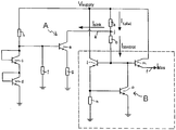
- FIG. 1 shows a circuit diagram of a preferred embodiment.
- the circuit shown in the diagram of the figure comprises a circuit A for the generation of the control current and, for the purpose of illustration only, an example of a standard bias circuit B.
- the control current I Ccontrol is fed into the bias circuit B from the supply voltage V supply via a control current line j.
- the control current line j comprises two resistors a and b, which are arranged in series and form a voltage divider.
- a sink current line k branches off from the control current line j between the resistors a, b.
- the sink current line k is provided for a correction current I sink , by which the total current I total through the resistor a is reduced to the control current I control through the resistor b.
- the correction current I sink is controlled in such a way that the control current I control is maintained on the preset value.
- the circuit A is provided, comprising a current sink transistor e and at least one reference transistor c, d.
- each reference transistor c, d is provided, both having their base and collector connected, so that each reference transistor c, d operates like a diode.
- the reference transistors c, d are arranged in series, and the collector of the first reference transistor c is connected between the resistors h and i, which form a further voltage divider.
- the emitter of the second reference transistor d is connected to ground.
- the collector of the first reference transistor c is connected to the base of a transistor e, the current sink transistor, which is provided to generate the correction current I sink .
- the collector of the current sink transistor e is therefore connected to the sink current line k, and the emitter of the current sink transistor e is connected to ground via the resistor g.
- the circuit A thus controls the value of the control current Icontrol, which is fed into the bias circuit B or into any other circuit using a stable current.
- the bias circuit B comprises three transistors. The bases of a first and a second one of these transistors 1, m are connected to one another, to the control current line j and to the collector of the third transistor o. The collectors of the first and second transistors 1, m are connected to the supply voltage. The emitter of the first transistor 1 is connected to ground via a further resistor n and to the base of the third transistor o. The emitter of the third transistor o is connected to ground, and the emitter of the second transistor m supplies a bias current f.
- the bias circuit B can be substituted with any other circuit that makes use of a control current or reference current. This is indicated in the figure by the rectangular frame of broken lines enclosing part B of the circuitry.
Landscapes
- Engineering & Computer Science (AREA)
- Microelectronics & Electronic Packaging (AREA)
- Physics & Mathematics (AREA)
- Nonlinear Science (AREA)
- Electromagnetism (AREA)
- General Physics & Mathematics (AREA)
- Radar, Positioning & Navigation (AREA)
- Automation & Control Theory (AREA)
- Control Of Electrical Variables (AREA)
- Amplifiers (AREA)
Claims (3)
- Circuit pour générer un courant de contrôle qui soit indépendant des variations de tension, comprenant :- une tension d'alimentation (Vsupply),- une ligne de contrôle de courant (j) comprenant deux résistances (a, b),- une ligne de courant de puits (k) dérivée à partir de la ligne de courant de contrôle entre les résistances, et- un transistor de puits de courant (e) possédant une base, un émetteur et un collecteur, le collecteur étant relié à la ligne de courant de puits et l'émetteur étant relié à la masse via une première autre résistance (g),caractérisé en ce que :- le circuit comprend en outre au moins un transistor de référence (c) possédant une base, un émetteur et un collecteur, le collecteur du transistor de référence étant relié à la base, à la tension d'alimentation via une deuxième autre résistance (h) et à la base du transistor de puits de courant, l'émetteur du transistor de référence étant relié à la masse ou à un autre transistor de référence (d) possédant une base, un émetteur et un collecteur, le collecteur de l'autre transistor de référence étant relié à l'émetteur du transistor de référence (c) et à la base de l'autre transistor de référence (d), et l'émetteur de l'autre transistor de référence étant relié à la masse, et- la base du transistor de puits de courant (e) et le collecteur de transistor de référence (c) sont reliés à la masse via une troisième autre résistance (i).
- Le circuit de la revendication 1, comprenant en outre :- un circuit de polarisation (B) basé sur un courant de référence (Icontrol), le circuit de polarisation étant relié à la tension d'alimentation (Vsupply) et à la ligne de courant de contrôle (j).
- Le circuit de la revendication 2, comprenant en outre :- trois transistors (1, m, o) du circuit de polarisation (B), chacun possédant une base, un émetteur et un collecteur,- les bases d'un premier et d'un deuxième de ces transistors (1, m) étant reliées les unes aux autres, à la ligne de courant de contrôle (j) et au collecteur du troisième transistor (o) du circuit de polarisation,- les collecteurs des premier et deuxième transistors (1, m) étant reliés à la tension d'alimentation (Vsupply),- l'émetteur du premier transistor (1) étant relié à la masse via une quatrième autre résistance (n) et à la base du troisième transistor (o),- l'émetteur du troisième transistor étant relié à la masse, et- l'émetteur du deuxième transistor (m) délivrant un courant de polarisation (f).
Priority Applications (4)
| Application Number | Priority Date | Filing Date | Title |
|---|---|---|---|
| EP08166350.2A EP2175342B1 (fr) | 2008-10-10 | 2008-10-10 | Circuit pour générer un courant de contrôle |
| PCT/EP2009/063212 WO2010040841A2 (fr) | 2008-10-10 | 2009-10-09 | Circuit de production d'un courant de commande |
| JP2011530503A JP5547202B2 (ja) | 2008-10-10 | 2009-10-09 | 制御電流生成回路 |
| US13/040,733 US8258858B2 (en) | 2008-10-10 | 2011-03-04 | Circuit for generating a control current |
Applications Claiming Priority (1)
| Application Number | Priority Date | Filing Date | Title |
|---|---|---|---|
| EP08166350.2A EP2175342B1 (fr) | 2008-10-10 | 2008-10-10 | Circuit pour générer un courant de contrôle |
Publications (2)
| Publication Number | Publication Date |
|---|---|
| EP2175342A1 EP2175342A1 (fr) | 2010-04-14 |
| EP2175342B1 true EP2175342B1 (fr) | 2017-05-03 |
Family
ID=40193825
Family Applications (1)
| Application Number | Title | Priority Date | Filing Date |
|---|---|---|---|
| EP08166350.2A Ceased EP2175342B1 (fr) | 2008-10-10 | 2008-10-10 | Circuit pour générer un courant de contrôle |
Country Status (4)
| Country | Link |
|---|---|
| US (1) | US8258858B2 (fr) |
| EP (1) | EP2175342B1 (fr) |
| JP (1) | JP5547202B2 (fr) |
| WO (1) | WO2010040841A2 (fr) |
Family Cites Families (5)
| Publication number | Priority date | Publication date | Assignee | Title |
|---|---|---|---|---|
| US4525663A (en) * | 1982-08-03 | 1985-06-25 | Burr-Brown Corporation | Precision band-gap voltage reference circuit |
| US5304918A (en) * | 1992-01-22 | 1994-04-19 | Samsung Semiconductor, Inc. | Reference circuit for high speed integrated circuits |
| US5793194A (en) * | 1996-11-06 | 1998-08-11 | Raytheon Company | Bias circuit having process variation compensation and power supply variation compensation |
| JP2008154043A (ja) * | 2006-12-19 | 2008-07-03 | Sharp Corp | バイアス回路、能動素子回路、および、電力増幅器 |
| JP2008172538A (ja) * | 2007-01-11 | 2008-07-24 | Sharp Corp | バイアス回路および電力増幅器 |
-
2008
- 2008-10-10 EP EP08166350.2A patent/EP2175342B1/fr not_active Ceased
-
2009
- 2009-10-09 WO PCT/EP2009/063212 patent/WO2010040841A2/fr not_active Ceased
- 2009-10-09 JP JP2011530503A patent/JP5547202B2/ja not_active Expired - Fee Related
-
2011
- 2011-03-04 US US13/040,733 patent/US8258858B2/en not_active Expired - Fee Related
Also Published As
| Publication number | Publication date |
|---|---|
| JP5547202B2 (ja) | 2014-07-09 |
| US8258858B2 (en) | 2012-09-04 |
| WO2010040841A3 (fr) | 2010-06-24 |
| EP2175342A1 (fr) | 2010-04-14 |
| JP2012505454A (ja) | 2012-03-01 |
| WO2010040841A2 (fr) | 2010-04-15 |
| US20110210714A1 (en) | 2011-09-01 |
Similar Documents
| Publication | Publication Date | Title |
|---|---|---|
| US8378657B2 (en) | Paralleling voltage regulators | |
| US7023181B2 (en) | Constant voltage generator and electronic equipment using the same | |
| US9395731B2 (en) | Circuit to reduce output capacitor of LDOs | |
| US7612613B2 (en) | Self regulating biasing circuit | |
| US9348347B2 (en) | Voltage generator with current source compensated for an error current operable over a wide voltage range | |
| US6201374B1 (en) | Voltage regulation and power switching system | |
| US6486724B2 (en) | FET bias circuit | |
| US20150084526A1 (en) | Systems and methods for current matching of led strings | |
| US20070159145A1 (en) | Compact voltage regulator | |
| EP2175342B1 (fr) | Circuit pour générer un courant de contrôle | |
| US7304541B2 (en) | Temperature compensated voltage regulator integrated with MMIC's | |
| US8624610B2 (en) | Synthesized current sense resistor for wide current sense range | |
| US20070200546A1 (en) | Reference voltage generating circuit for generating low reference voltages | |
| JP2009093446A (ja) | 電圧制御回路 | |
| US11095260B2 (en) | Amplifier with low drift biasing | |
| US20090039945A1 (en) | Bias Current Generator | |
| US7012410B2 (en) | Regulating system | |
| US20110175447A1 (en) | Current Control System and Method for Controlling a Current | |
| US7362166B2 (en) | Apparatus for polarity-inversion-protected supplying of an electronic component with an intermediate voltage from a supply voltage | |
| JP2003298349A (ja) | 電圧制御型発振回路 | |
| JP2000339046A (ja) | シャントレギュレータ | |
| US7091787B2 (en) | Transconductance amplifier with temperature sensitive current limiting | |
| US20190384344A1 (en) | Circuit for Generating a Negative Higher Order Temperature Coefficient Current | |
| JP2008021206A (ja) | ボルテージレギュレータ | |
| JP2003198269A (ja) | 増幅装置及びそれを用いた通信装置 |
Legal Events
| Date | Code | Title | Description |
|---|---|---|---|
| PUAI | Public reference made under article 153(3) epc to a published international application that has entered the european phase |
Free format text: ORIGINAL CODE: 0009012 |
|
| AK | Designated contracting states |
Kind code of ref document: A1 Designated state(s): AT BE BG CH CY CZ DE DK EE ES FI FR GB GR HR HU IE IS IT LI LT LU LV MC MT NL NO PL PT RO SE SI SK TR |
|
| AX | Request for extension of the european patent |
Extension state: AL BA MK RS |
|
| 17P | Request for examination filed |
Effective date: 20101004 |
|
| 17Q | First examination report despatched |
Effective date: 20101122 |
|
| AKX | Designation fees paid |
Designated state(s): DE |
|
| GRAP | Despatch of communication of intention to grant a patent |
Free format text: ORIGINAL CODE: EPIDOSNIGR1 |
|
| INTG | Intention to grant announced |
Effective date: 20161102 |
|
| GRAS | Grant fee paid |
Free format text: ORIGINAL CODE: EPIDOSNIGR3 |
|
| GRAA | (expected) grant |
Free format text: ORIGINAL CODE: 0009210 |
|
| RAP1 | Party data changed (applicant data changed or rights of an application transferred) |
Owner name: SNAPTRACK, INC. |
|
| AK | Designated contracting states |
Kind code of ref document: B1 Designated state(s): DE |
|
| REG | Reference to a national code |
Ref country code: DE Ref legal event code: R096 Ref document number: 602008050026 Country of ref document: DE |
|
| REG | Reference to a national code |
Ref country code: DE Ref legal event code: R097 Ref document number: 602008050026 Country of ref document: DE |
|
| PLBE | No opposition filed within time limit |
Free format text: ORIGINAL CODE: 0009261 |
|
| STAA | Information on the status of an ep patent application or granted ep patent |
Free format text: STATUS: NO OPPOSITION FILED WITHIN TIME LIMIT |
|
| 26N | No opposition filed |
Effective date: 20180206 |
|
| PGFP | Annual fee paid to national office [announced via postgrant information from national office to epo] |
Ref country code: DE Payment date: 20190917 Year of fee payment: 12 |
|
| REG | Reference to a national code |
Ref country code: DE Ref legal event code: R119 Ref document number: 602008050026 Country of ref document: DE |
|
| PG25 | Lapsed in a contracting state [announced via postgrant information from national office to epo] |
Ref country code: DE Free format text: LAPSE BECAUSE OF NON-PAYMENT OF DUE FEES Effective date: 20210501 |