EP2175489A1 - Halbleiterbauelement - Google Patents
Halbleiterbauelement Download PDFInfo
- Publication number
- EP2175489A1 EP2175489A1 EP08764759A EP08764759A EP2175489A1 EP 2175489 A1 EP2175489 A1 EP 2175489A1 EP 08764759 A EP08764759 A EP 08764759A EP 08764759 A EP08764759 A EP 08764759A EP 2175489 A1 EP2175489 A1 EP 2175489A1
- Authority
- EP
- European Patent Office
- Prior art keywords
- column
- diffusion layer
- semiconductor device
- island
- cmos
- Prior art date
- Legal status (The legal status is an assumption and is not a legal conclusion. Google has not performed a legal analysis and makes no representation as to the accuracy of the status listed.)
- Granted
Links
Images


Classifications
-
- H—ELECTRICITY
- H10—SEMICONDUCTOR DEVICES; ELECTRIC SOLID-STATE DEVICES NOT OTHERWISE PROVIDED FOR
- H10D—INORGANIC ELECTRIC SEMICONDUCTOR DEVICES
- H10D84/00—Integrated devices formed in or on semiconductor substrates that comprise only semiconducting layers, e.g. on Si wafers or on GaAs-on-Si wafers
- H10D84/80—Integrated devices formed in or on semiconductor substrates that comprise only semiconducting layers, e.g. on Si wafers or on GaAs-on-Si wafers characterised by the integration of at least one component covered by groups H10D12/00 or H10D30/00, e.g. integration of IGFETs
- H10D84/82—Integrated devices formed in or on semiconductor substrates that comprise only semiconducting layers, e.g. on Si wafers or on GaAs-on-Si wafers characterised by the integration of at least one component covered by groups H10D12/00 or H10D30/00, e.g. integration of IGFETs of only field-effect components
- H10D84/83—Integrated devices formed in or on semiconductor substrates that comprise only semiconducting layers, e.g. on Si wafers or on GaAs-on-Si wafers characterised by the integration of at least one component covered by groups H10D12/00 or H10D30/00, e.g. integration of IGFETs of only field-effect components of only insulated-gate FETs [IGFET]
- H10D84/85—Complementary IGFETs, e.g. CMOS
-
- H—ELECTRICITY
- H10—SEMICONDUCTOR DEVICES; ELECTRIC SOLID-STATE DEVICES NOT OTHERWISE PROVIDED FOR
- H10D—INORGANIC ELECTRIC SEMICONDUCTOR DEVICES
- H10D84/00—Integrated devices formed in or on semiconductor substrates that comprise only semiconducting layers, e.g. on Si wafers or on GaAs-on-Si wafers
- H10D84/01—Manufacture or treatment
- H10D84/0123—Integrating together multiple components covered by H10D12/00 or H10D30/00, e.g. integrating multiple IGBTs
- H10D84/0126—Integrating together multiple components covered by H10D12/00 or H10D30/00, e.g. integrating multiple IGBTs the components including insulated gates, e.g. IGFETs
- H10D84/0165—Integrating together multiple components covered by H10D12/00 or H10D30/00, e.g. integrating multiple IGBTs the components including insulated gates, e.g. IGFETs the components including complementary IGFETs, e.g. CMOS devices
- H10D84/0172—Manufacturing their gate conductors
- H10D84/0179—Manufacturing their gate conductors the gate conductors having different shapes or dimensions
-
- H—ELECTRICITY
- H10—SEMICONDUCTOR DEVICES; ELECTRIC SOLID-STATE DEVICES NOT OTHERWISE PROVIDED FOR
- H10D—INORGANIC ELECTRIC SEMICONDUCTOR DEVICES
- H10D84/00—Integrated devices formed in or on semiconductor substrates that comprise only semiconducting layers, e.g. on Si wafers or on GaAs-on-Si wafers
- H10D84/01—Manufacture or treatment
- H10D84/0123—Integrating together multiple components covered by H10D12/00 or H10D30/00, e.g. integrating multiple IGBTs
- H10D84/0126—Integrating together multiple components covered by H10D12/00 or H10D30/00, e.g. integrating multiple IGBTs the components including insulated gates, e.g. IGFETs
- H10D84/0165—Integrating together multiple components covered by H10D12/00 or H10D30/00, e.g. integrating multiple IGBTs the components including insulated gates, e.g. IGFETs the components including complementary IGFETs, e.g. CMOS devices
- H10D84/0188—Manufacturing their isolation regions
-
- H—ELECTRICITY
- H10—SEMICONDUCTOR DEVICES; ELECTRIC SOLID-STATE DEVICES NOT OTHERWISE PROVIDED FOR
- H10D—INORGANIC ELECTRIC SEMICONDUCTOR DEVICES
- H10D84/00—Integrated devices formed in or on semiconductor substrates that comprise only semiconducting layers, e.g. on Si wafers or on GaAs-on-Si wafers
- H10D84/01—Manufacture or treatment
- H10D84/0123—Integrating together multiple components covered by H10D12/00 or H10D30/00, e.g. integrating multiple IGBTs
- H10D84/0126—Integrating together multiple components covered by H10D12/00 or H10D30/00, e.g. integrating multiple IGBTs the components including insulated gates, e.g. IGFETs
- H10D84/0165—Integrating together multiple components covered by H10D12/00 or H10D30/00, e.g. integrating multiple IGBTs the components including insulated gates, e.g. IGFETs the components including complementary IGFETs, e.g. CMOS devices
- H10D84/0195—Integrating together multiple components covered by H10D12/00 or H10D30/00, e.g. integrating multiple IGBTs the components including insulated gates, e.g. IGFETs the components including complementary IGFETs, e.g. CMOS devices the components including vertical IGFETs
-
- H—ELECTRICITY
- H10—SEMICONDUCTOR DEVICES; ELECTRIC SOLID-STATE DEVICES NOT OTHERWISE PROVIDED FOR
- H10D—INORGANIC ELECTRIC SEMICONDUCTOR DEVICES
- H10D84/00—Integrated devices formed in or on semiconductor substrates that comprise only semiconducting layers, e.g. on Si wafers or on GaAs-on-Si wafers
- H10D84/01—Manufacture or treatment
- H10D84/02—Manufacture or treatment characterised by using material-based technologies
- H10D84/03—Manufacture or treatment characterised by using material-based technologies using Group IV technology, e.g. silicon technology or silicon-carbide [SiC] technology
- H10D84/038—Manufacture or treatment characterised by using material-based technologies using Group IV technology, e.g. silicon technology or silicon-carbide [SiC] technology using silicon technology, e.g. SiGe
-
- H—ELECTRICITY
- H10—SEMICONDUCTOR DEVICES; ELECTRIC SOLID-STATE DEVICES NOT OTHERWISE PROVIDED FOR
- H10D—INORGANIC ELECTRIC SEMICONDUCTOR DEVICES
- H10D86/00—Integrated devices formed in or on insulating or conducting substrates, e.g. formed in silicon-on-insulator [SOI] substrates or on stainless steel or glass substrates
- H10D86/01—Manufacture or treatment
-
- H—ELECTRICITY
- H10—SEMICONDUCTOR DEVICES; ELECTRIC SOLID-STATE DEVICES NOT OTHERWISE PROVIDED FOR
- H10D—INORGANIC ELECTRIC SEMICONDUCTOR DEVICES
- H10D30/00—Field-effect transistors [FET]
- H10D30/60—Insulated-gate field-effect transistors [IGFET]
- H10D30/67—Thin-film transistors [TFT]
- H10D30/6728—Vertical TFTs
Definitions
- the present invention relates to a semiconductor device.
- SGT surrounding gate transistor having a structure in which a source, a gate and a drain are arranged in a direction perpendicular to a substrate, wherein the gate is formed to surround an island-shaped semiconductor layer, and a CMOS inverter circuit using the SGT (see, for example, the following Patent Documents 1 to 3).
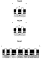
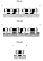
- FIGS. 1(a) and 1(b) show a conventional SGT-based two-stage CMOS inverter configured to input an output of a first inverter into a second inverter (see the following Non-Patent Document 1).
- a sectional view of the two-stage CMOS inverter is shown in FIGS. 2(b) and 2(c) .
- the first inverter is made up of two pMOS SGTs 01, 02 and one nMOS SGT 03.
- the second inverter is made up of two pMOS SGTs 04, 05 and two nMOS SGTs 06, 07.
- the conventional SGT-based two-stage CMOS inverter employs a structure where a first power supply potential Vss and a second power supply potential Vcc are supplied to SGTs from respective ones of a first power supply line (Vss line) Vssl and a second power supply line (Vcc line) Vccl via corresponding ones of drain and source diffusion layers in a silicon substrate and through a plurality of contacts.
- the power supply lines for the nMOS and pMOS SGTs are arranged on one side of a lower portion of a gate region which is different from an on-substrate region where the nMOS and pMOS SGTs are arranged.
- a resistance of a diffusion layer is extremely larger than that of a metal line for power supply. If a resistance of the first power supply line Vssl and the second power supply line Vccl increases, a source potential to be applied to each of the nMOS SGTs will increase relative to the first power supply potential Vss, and a source potential to be supplied to each of the pMOS SGTs will decrease relative to the second power supply potential Vcc. The increase in source potential of the nMOS SGT relative to the first power supply potential Vss leads to a decrease in drive current of the nMOS SGT.
- the decrease in source potential of the pMOS SGT relative to the second power supply potential Vcc leads to a decrease in drive current of the pMOS SGT.
- the decrease in drive current of each of the SGTs leads to a decrease in charge/discharge rate of a capacitance in an output terminal of the inverter.
- the decrease in charge/discharge rate of the capacitance in an output terminal of the inverter leads to an increase in delay time of the inverter. Therefore, a metal line is connected to the diffusion layer through a large number of contacts to apply the first power supply potential Vss to a source of each of the nMOS SGTs and apply the second power supply potential Vcc to a source of each of the pMOS SGTs.
- a contact is arranged on the drain diffusion layer and connected to a metal line to form an output section of the first inverter.
- the metal line in the output section of the first inverter is connected to a polysilicon gate as an input section of the second inverter through a contact.
- the pMOS SGT is required to have a gate width two times greater than that of the nMOS SGT, because a hole mobility is one-half of an electron mobility.
- a semiconductor device which comprises a CMOS inverter cascade circuit having a plurality of CMOS inverters cascade-connected in at least two stages, wherein the CMOS inverter cascade circuit includes a first CMOS inverter and a second CMOS inverter which are formed as a two-stage CMOS inverter made up of six MOS transistors arranged on a substrate in a two-row by three-column array, and wherein: each of two MOS transistors in a respective one of the 1st column and the 3rd column is a p-channel MOS transistor; and two MOS transistors in the 2nd column is an n-channel MOS transistor, and wherein each of the p-channel MOS transistors and the n-channel MOS transistors has a structure where a drain, a source and a gate thereof are arranged in a direction perpendicular to the substrate while allowing the gate to
- the CMOS inverter cascade circuit includes a (2 ⁇ N)-stage CMOS inverter having a number N of the two-stage CMOS inverters arranged on the substrate in a row direction (wherein N is an integer of 2 or more), and wherein: each of the first-CMOS-inverter output terminal and the second-CMOS-inverter output terminal is connected to a respective one of the second-CMOS-inverter input terminal and the first-CMOS-inverter input terminal adjacent thereto; and the second power supply lines arranged on the source diffusion layers of adjacent four of the p-channel MOS transistors are connected to each other on the source diffusion layers of the adjacent four p-channel MOS transistors.
- the CMOS inverter cascade circuit includes, on the substrate, a CMOS inverter array configured such that a number N of the two-stage CMOS inverters are arranged in a row direction, and a number M of the two-stage CMOS inverters are arranged in a column direction (wherein N is an integer of 2 or more, and M is an integer of 2 or more), and wherein the second power supply lines provided for respective ones of the M first CMOS inverters arranged in the column direction are connected to each other on the source diffusion layers of the p-channel MOS transistors in the M first CMOS inverters; the second power supply lines provided for respective ones of the M second CMOS inverters arranged in the column direction are connected to each other on the source diffusion layers of the p-channel MOS transistors in the M second CMOS inverters; and the first power supply lines provided for respective ones of the M first CMOS inverters arranged in the column direction, and the first power supply lines
- the CMOS inverter cascade circuit has, on the substrate, a CMOS inverter array configured such that a number N of the two-stage CMOS inverters are arranged in a row direction, and a number M of the two-stage CMOS inverters are arranged in a column direction (wherein N is an integer of 2 or more, and M is an integer of 2 or more, and wherein: the first power supply lines provided for respective ones of the first and second CMOS inverters successively arranged in the column direction are connected to each other on the source diffusion layers of the n-channel MOS transistors of the first and second CMOS inverters over the column direction; the second power supply lines provided for respective ones of the first and second CMOS inverters successively arranged in the column direction are connected to each other on the source diffusion layers of the p-channel MOS transistors of the first CMOS inverters over the column direction; the second power supply lines provided for respective ones of a part of the first and
- the present invention provides a semiconductor device which comprises a CMOS inverter cascade circuit having a plurality of CMOS inverters cascade-connected in at least two stages, wherein the CMOS inverter cascade circuit includes a first CMOS inverter and a second CMOS inverter.
- the first CMOS inverter comprises: an n-channel semiconductor device formed in a structure where a drain, a source and a gate thereof are arranged in a direction perpendicular to a substrate while allowing the gate to surround an island-shaped semiconductor layer, and arranged at an intersection of the 1st row and the 2nd column; a p-channel semiconductor device formed in a structure where a drain, a source and a gate thereof are arranged in a direction perpendicular to the substrate while allowing the gate to surround an island-shaped semiconductor layer, and arranged at an intersection of the 1st row and the 1st column; a p-channel semiconductor device formed in a structure where a drain, a source and a gate thereof are arranged in a direction perpendicular to the substrate while allowing the gate to surround an island-shaped semiconductor layer, and arranged at an intersection of the 2nd row and the 1st column; a first-CMOS-inverter input terminal arranged to interconnect the gate of the n-channel semiconductor device
- the second CMOS inverter comprises: an n-channel semiconductor device formed in a structure where a drain, a source and a gate thereof are arranged in a direction perpendicular to the substrate while allowing the gate to surround an island-shaped semiconductor layer, and arranged at an intersection of the 2nd row and the 2nd column; a p-channel semiconductor device formed in a structure where a drain, a source and a gate thereof are arranged in a direction perpendicular to the substrate while allowing the gate to surround an island-shaped semiconductor layer, and arranged at an intersection of the 1st row and the 3rd column; a p-channel semiconductor device formed in a structure where a drain, a source and a gate thereof are arranged in a direction perpendicular to the substrate while allowing the gate to surround an island-shaped semiconductor layer, and arranged at an intersection of the 2nd row and the 3rd column; a second-CMOS-inverter input terminal arranged to interconnect the gate of the n-channel semiconductor device at the
- the first-CMOS-inverter output terminal is connected to the second-CMOS-inverter input terminal.
- a first power supply line Vssl is connected to a source diffusion layer of the n-channel semiconductor device of the first CMOS inverter; a first power supply line Vssl is connected to a source diffusion layer of the n-channel semiconductor device of the second CMOS inverter; a second power supply line Vccl is connected to a source diffusion layer of each of the two p-channel semiconductor devices of the first CMOS inverter; and a second power supply line Vccl is connected to a source diffusion layer of each of the two p-channel semiconductor devices of the second CMOS inverter.
- the present invention also provides a semiconductor device which comprises a CMOS inverter cascade circuit having a plurality of CMOS inverters cascade-connected in at least two stages, wherein the CMOS inverter cascade circuit includes a first CMOS inverter, a second CMOS inverter, a third CMOS inverter and a fourth CMOS inverter.
- the first CMOS inverter comprises: an n-channel semiconductor device formed in a structure where a drain, a source and a gate thereof are arranged in a direction perpendicular to a substrate while allowing the gate to surround an island-shaped semiconductor layer, and arranged at an intersection of the 1st row and the 2nd column; a p-channel semiconductor device formed in a structure where a drain, a source and a gate thereof are arranged in a direction perpendicular to the substrate while allowing the gate to surround an island-shaped semiconductor layer, and arranged at an intersection of the 1st row and the 1st column; a p-channel semiconductor device formed in a structure where a drain, a source and a gate thereof are arranged in a direction perpendicular to the substrate while allowing the gate to surround an island-shaped semiconductor layer, and arranged at an intersection of the 2nd row and the 1st column; a first-CMOS-inverter input terminal arranged to interconnect the gate of the n-channel semiconductor device
- the second CMOS inverter comprises: an n-channel semiconductor device formed in a structure where a drain, a source and a gate thereof are arranged in a direction perpendicular to the substrate while allowing the gate to surround an island-shaped semiconductor layer, and arranged at an intersection of the 2nd row and the 2nd column; a p-channel semiconductor device formed in a structure where a drain, a source and a gate thereof are arranged in a direction perpendicular to the substrate while allowing the gate to surround an island-shaped semiconductor layer, and arranged at an intersection of the 1st row and the 3rd column; a p-channel semiconductor device formed in a structure where a drain, a source and a gate thereof are arranged in a direction perpendicular to the substrate while allowing the gate to surround an island-shaped semiconductor layer, and arranged at an intersection of the 2nd row and the 3rd column; a second-CMOS-inverter input terminal arranged to interconnect the gate of the n-channel semiconductor device at the
- the third CMOS inverter comprises: an n-channel semiconductor device formed in a structure where a drain, a source and a gate thereof are arranged in a direction perpendicular to a substrate while allowing the gate to surround an island-shaped semiconductor layer, and arranged at an intersection of the 1st row and the 5th column; a p-channel semiconductor device formed in a structure where a drain, a source and a gate thereof are arranged in a direction perpendicular to the substrate while allowing the gate to surround an island-shaped semiconductor layer, and arranged at an intersection of the 1st row and the 4th column; a p-channel semiconductor device formed in a structure where a drain, a source and a gate thereof are arranged in a direction perpendicular to the substrate while allowing the gate to surround an island-shaped semiconductor layer, and arranged at an intersection of the 2nd row and the 4th column; a third-CMOS-inverter input terminal arranged to interconnect the gate of the n-channel semiconductor device at the
- the fourth CMOS inverter comprises: an n-channel semiconductor device formed in a structure where a drain, a source and a gate thereof are arranged in a direction perpendicular to the substrate while allowing the gate to surround an island-shaped semiconductor layer, and arranged at an intersection of the 2nd row and the 5th column; a p-channel semiconductor device formed in a structure where a drain, a source and a gate thereof are arranged in a direction perpendicular to the substrate while allowing the gate to surround an island-shaped semiconductor layer, and arranged at an intersection of the 1st row and the 6th column; a p-channel semiconductor device formed in a structure where a drain, a source and a gate thereof are arranged in a direction perpendicular to the substrate while allowing the gate to surround an island-shaped semiconductor layer, and arranged at an intersection of the 2nd row and the 6th column; a fourth-CMOS-inverter input terminal arranged to interconnect the gate of the n-channel semiconductor device at the intersection of
- the first-CMOS-inverter output terminal is connected to the second-CMOS-inverter input terminal. Further, the second-CMOS-inverter output terminal is connected to the third-CMOS-inverter input terminal, and the third-CMOS-inverter output terminal is connected to the fourth-CMOS-inverter input terminal.
- a first power supply line Vssl is connected to a source diffusion layer of the n-channel semiconductor device of the first CMOS inverter; a first power supply line Vssl is connected to a source diffusion layer of the n-channel semiconductor device of the second CMOS inverter; a first power supply line Vssl is connected to a source diffusion layer of the n-channel semiconductor device of the third CMOS inverter; a first power supply line Vssl is connected to a source diffusion layer of the n-channel semiconductor device of the fourth CMOS inverter; a second power supply line Vccl is connected to a source diffusion layer of each of the two p-channel semiconductor devices of the first CMOS inverter; a second power supply line Vccl is connected to a source diffusion layer of each of the two p-channel semiconductor devices of the second CMOS inverter; a second power supply line Vccl is connected to a source diffusion layer of each of the two p-channel semiconductor devices of the third
- an n-channel MOS transistor for use in the above semiconductor device.
- the n-channel MOS transistor comprises: a drain, a gate and a source which are arranged in a direction perpendicular to a substrate while allowing the gate to surround an island-shaped semiconductor layer; a dielectric layer formed above and below the gate; a polysilicon line formed as an island-shaped semiconductor lower layer to surround a part of a drain diffusion layer; and a metal line formed on a source diffusion layer, wherein each of the drain diffusion layer, the polysilicon line, the gate and the source diffusion layer has a salicided structure.
- a p-channel MOS transistor for use in the above semiconductor device.
- the p-channel MOS transistor comprises: a drain, a gate and a source which are arranged in a direction perpendicular to a substrate while allowing the gate to surround an island-shaped semiconductor layer; a dielectric layer formed above and below the gate; a polysilicon line formed as an island-shaped semiconductor lower layer to surround a part of a drain diffusion layer; and a metal line formed on a source diffusion layer, wherein each of the drain diffusion layer, the polysilicon line, the gate and the source diffusion layer has a salicided structure.
- the conventional SGT-based two-stage CMOS inverter employs a structure where a first power supply potential Vss and a second power supply potential Vcc are supplied to respective diffusion layers in a silicon substrate SGTs through a plurality of contacts.
- two power supply lines for the nMOS and pMOS SGTs are arranged on one side of a lower portion of a gate region which is different from an on-substrate region where nMOS and pMOS layers are arranged.
- the semiconductor device of the present invention comprises a first power supply line Vssl and a second power supply line Vccl each arranged to supply a respective one of a first power supply potential Vss and a second power supply potential Vcc to a corresponding one of an nMOS SGT and a pMOS SGT from thereabove, wherein: the first power supply line Vssl includes a first power supply line Vssl connected to a source diffusion layer of an n-channel semiconductor device in a first inverter, and a first power supply line Vssl connected to a source diffusion layer of an n-channel semiconductor device in a second inverter; and the second power supply line Vccl includes a second power supply line Vccl connected to respective source diffusion layers of two p-channel semiconductor devices in the first inverter, and a second power supply line Vccl connected to respective source diffusion layers of two p-channel semiconductor device in the second inverter.
- the first power supply line Vssl includes a
- each of the first power supply line Vssl and the second power supply line Vccl is arranged to supply a respective one of a first power supply potential Vss and a second power supply potential Vcc to a corresponding one of an nMOS SGT and a pMOS SGT from thereabove, wherein: the first power supply line Vssl includes a first power supply line Vssl connected to a source diffusion layer of an n-channel semiconductor device in a first inverter, and a first power supply line Vssl connected to a source diffusion layer of an n-channel semiconductor device in a second inverter; and the second power supply line Vccl includes a second power supply line Vccl connected to respective source diffusion layers of two p-channel semiconductor devices in the first inverter, and a second power supply line Vccl connected to respective source diffusion layers of two p-channel semiconductor device in the second inverter, makes it possible reduce a resistance of the first power supply line Vs
- the semiconductor device of the present invention comprises an output terminal arranged to interconnect the drain diffusion layer of the n-channel semiconductor device and the drain diffusion layers of the p-channel semiconductor devices, through an island-shaped semiconductor lower layer.
- the two p-MOS SGTs of the first inverter are arranged at respective ones of the intersection of the 1st row and the 1st column and the intersection of the 2nd row and the 1st column, and the n-MOS SGT of the first inverter is arranged at the intersection of the 1st row and the 2nd column.
- the two p-MOS SGTs of the second inverter are arranged at respective ones of the intersection of the 1st row and the 3rd column and the intersection of the 2nd row and the 3rd column, and the n-MOS SGT of the second inverter is arranged at the intersection of the 2nd row and the 2nd column.
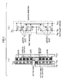
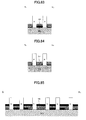
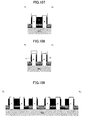
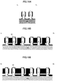
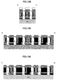
- FIGS. 3 to 7 show a layout and a cross-sectional structure of a semiconductor device according to a first embodiment of the present invention.
- one n-channel semiconductor device (n-channel MOS transistor) is arranged at an intersection of the 1st row and the 2nd column, wherein the n-channel semiconductor device comprises: an output terminal line 19 based on an island-shaped semiconductor lower layer (island-shaped semiconductor lower layer-based line 19), and a drain diffusion layer 9, each formed on a silicon oxide film 8 of a substrate; an island-shaped semiconductor layer 10 formed on the drain diffusion layer 9; a source diffusion layer 11 formed on top of the island-shaped semiconductor layer 10; and a gate 12 formed on a channel region of a sidewall of the island-shaped semiconductor layer 10 sandwiched between the drain diffusion layer 9 and the source diffusion layer 11, through a gate dielectric film.
- the n-channel semiconductor device comprises: an output terminal line 19 based on an island-shaped semiconductor lower layer (island-shaped semiconductor lower layer-based line 19), and a drain diffusion layer 9, each formed on a silicon oxide film 8 of a substrate; an island-shaped semiconductor layer 10 formed on the drain diffusion layer 9; a source diffusion
- One of two p-channel semiconductor devices is arranged at an intersection of the 1st row and the 1st column, wherein the p-channel semiconductor device comprises: the island-shaped semiconductor lower layer-based line 19 and a drain diffusion layer 13 each formed on the silicon oxide film 8; an island-shaped semiconductor layer 14 formed on the drain diffusion layer 13; a source diffusion layer 15 formed on top of the island-shaped semiconductor layer 14; and the gate 12 formed on a channel region of a sidewall of the island-shaped semiconductor layer 14 sandwiched between the drain diffusion layer 13 and the source diffusion layer 15, through a gate dielectric film.
- the p-channel semiconductor device comprises: the island-shaped semiconductor lower layer-based line 19 and a drain diffusion layer 13 each formed on the silicon oxide film 8; an island-shaped semiconductor layer 14 formed on the drain diffusion layer 13; a source diffusion layer 15 formed on top of the island-shaped semiconductor layer 14; and the gate 12 formed on a channel region of a sidewall of the island-shaped semiconductor layer 14 sandwiched between the drain diffusion layer 13 and the source diffusion layer 15,
- the other p-channel semiconductor device is arranged at an intersection of the 2nd row and the 1st column, wherein the p-channel the semiconductor device comprises: the island-shaped semiconductor lower layer-based line 19 and a drain diffusion layer 16 each formed on the silicon oxide film 8; an island-shaped semiconductor layer 17 formed on the drain diffusion layer 16; a source diffusion layer 18 formed on top of the island-shaped semiconductor layer 17; and the gate 12 formed on a channel region of a sidewall of the island-shaped semiconductor layer 17 sandwiched between the drain diffusion layer 16 and the source diffusion layer 18, through a gate dielectric film.
- the two p-channel semiconductor devices and the one n-channel semiconductor device make up a first inverter.
- one n-channel semiconductor device is arranged at an intersection of the 2nd row and the 2nd column, wherein the n-channel semiconductor device comprises: an output terminal line 30 based on an island-shaped semiconductor lower layer (island-shaped semiconductor lower layer-based line 30), and a drain diffusion layer 20, each formed on the silicon oxide film 8; an island-shaped semiconductor layer 21 formed on the drain diffusion layer 20; a source diffusion layer 22 formed on top of the island-shaped semiconductor layer 21; and a gate 23 formed on a channel region of a sidewall of the island-shaped semiconductor layer 21 sandwiched between the drain diffusion layer 20 and the source diffusion layer 22, through a gate dielectric film.
- the n-channel semiconductor device comprises: an output terminal line 30 based on an island-shaped semiconductor lower layer (island-shaped semiconductor lower layer-based line 30), and a drain diffusion layer 20, each formed on the silicon oxide film 8; an island-shaped semiconductor layer 21 formed on the drain diffusion layer 20; a source diffusion layer 22 formed on top of the island-shaped semiconductor layer 21; and a gate 23
- One of two p-channel semiconductor devices is arranged at an intersection of the 1st row and the 3rd column, wherein the p-channel semiconductor device comprises: the island-shaped semiconductor lower layer-based line 30 and a drain diffusion layer 27 each formed on the silicon oxide film 8; an island-shaped semiconductor layer 28 formed on the drain diffusion layer 27; a source diffusion layer 29 formed on top of the island-shaped semiconductor layer 28; and the gate 23 formed on a channel region of a sidewall of the island-shaped semiconductor layer 28 sandwiched between the drain diffusion layer 27 and the source diffusion layer 29, through a gate dielectric film.
- the other p-channel semiconductor device is arranged at an intersection of the 2nd row and the 3rd column, wherein the p-channel semiconductor device comprises: the island-shaped semiconductor lower layer-based line 30 and a drain diffusion layer 24 each formed on the silicon oxide film 8; an island-shaped semiconductor layer 25 formed on the drain diffusion layer 24; a source diffusion layer 26 formed on top of the island-shaped semiconductor layer 25; and the gate 23 formed on a channel region of a sidewall of the island-shaped semiconductor layer 25 sandwiched between the drain diffusion layer 24 and the source diffusion layer 25, through a gate dielectric film.
- the two p-channel semiconductor devices and the one n-channel semiconductor device make up a second inverter.
- one n-channel semiconductor device is arranged at an intersection of the 1st row and the 5th column, wherein the n-channel semiconductor device comprises: an output terminal line 41 based on an island-shaped semiconductor lower layer (island-shaped semiconductor lower layer-based line 41), and a drain diffusion layer 31, each formed on the silicon oxide film 8; an island-shaped semiconductor layer 32 formed on the drain diffusion layer 31; a source diffusion layer 33 formed on top of the island-shaped semiconductor layer 32; and a gate 34 formed on a channel region of a sidewall of the island-shaped semiconductor layer 32 sandwiched between the drain diffusion layer 31 and the source diffusion layer 33, through a gate dielectric film.
- the n-channel semiconductor device comprises: an output terminal line 41 based on an island-shaped semiconductor lower layer (island-shaped semiconductor lower layer-based line 41), and a drain diffusion layer 31, each formed on the silicon oxide film 8; an island-shaped semiconductor layer 32 formed on the drain diffusion layer 31; a source diffusion layer 33 formed on top of the island-shaped semiconductor layer 32; and a
- One of two p-channel semiconductor devices is arranged at an intersection of the 1st row and the 4th column, wherein the p-channel semiconductor device comprises: the island-shaped semiconductor lower layer-based line 41 and a drain diffusion layer 38 each formed on the silicon oxide film 8; an island-shaped semiconductor layer 39 formed on the drain diffusion layer 38; a source diffusion layer 40 formed on top of the island-shaped semiconductor layer 39; and the gate 34 formed on a channel region of a sidewall of the island-shaped semiconductor layer 39 sandwiched between the drain diffusion layer 38 and the source diffusion layer 40, through a gate dielectric film.
- the other p-channel semiconductor device is arranged at an intersection of the 2nd row and the 4th column, wherein the p-channel semiconductor device comprises: the island-shaped semiconductor lower layer-based line 41 and a drain diffusion layer 35 each formed on the silicon oxide film 8; an island-shaped semiconductor layer 36 formed on the drain diffusion layer 35; a source diffusion layer 37 formed on top of the island-shaped semiconductor layer 36; and the gate 34 formed on a channel region of a sidewall of the island-shaped semiconductor layer 36 sandwiched between the drain diffusion layer 35 and the source diffusion layer 37, through a gate dielectric film.
- the two p-channel semiconductor devices and the one n-channel semiconductor device make up a third inverter.
- one n-channel semiconductor device is arranged at an intersection of the 2nd row and the 5th column, wherein the n-channel semiconductor device comprises: an output terminal line 52 based on an island-shaped semiconductor lower layer (island-shaped semiconductor lower layer-based line 52), and a drain diffusion layer 42, each formed on the silicon oxide film 8; an island-shaped semiconductor layer 43 formed on the drain diffusion layer 42; a source diffusion layer 44 formed on top of the island-shaped semiconductor layer 43; and a gate 45 formed on a channel region of a sidewall of the island-shaped semiconductor layer 43 sandwiched between the drain diffusion layer 42 and the source diffusion layer 44, through a gate dielectric film.
- the n-channel semiconductor device comprises: an output terminal line 52 based on an island-shaped semiconductor lower layer (island-shaped semiconductor lower layer-based line 52), and a drain diffusion layer 42, each formed on the silicon oxide film 8; an island-shaped semiconductor layer 43 formed on the drain diffusion layer 42; a source diffusion layer 44 formed on top of the island-shaped semiconductor layer 43; and
- One of two p-channel semiconductor devices is arranged at an intersection of the 1st row and the 6th column, wherein the p-channel semiconductor device comprises: the island-shaped semiconductor lower layer-based line 52 and a drain diffusion layer 49 each formed on the silicon oxide film 8; an island-shaped semiconductor layer 50 formed on the drain diffusion layer 49; a source diffusion layer 51 formed on top of the island-shaped semiconductor layer 50; and the gate 45 formed on a channel region of a sidewall of the island-shaped semiconductor layer 50 sandwiched between the drain diffusion layer 49 and the source diffusion layer 51, through a gate dielectric film.
- the other p-channel semiconductor device is arranged at an intersection of the 2nd row and the 6th column, wherein the p-channel semiconductor device comprises: the island-shaped semiconductor lower layer-based line 52 and a drain diffusion layer 46 each formed on the silicon oxide film 8; an island-shaped semiconductor layer 47 formed on the drain diffusion layer 46; a source diffusion layer 48 formed on top of the island-shaped semiconductor layer 47; and the gate 45 formed on a channel region of a sidewall of the island-shaped semiconductor layer 47 sandwiched between the drain diffusion layer 46 and the source diffusion layer 48, through a gate dielectric film.
- the two p-channel semiconductor devices and the one n-channel semiconductor device make up a fourth inverter.
- a first power supply line Vssl 57 as a Vss line is formed on the source diffusion layers 11, 22 of the two n-channel semiconductor devices of the first and second inverters, and a first power supply line Vssl 59 as a Vss line is formed on the source diffusion layers 33, 44 of the two n-channel semiconductor devices of the third and fourth inverters. Further, a second power supply line Vccl 56 as a Vcc line is formed on the source diffusion layers 15, 18 of the two p-channel semiconductor devices of the first inverter.
- a second power supply line Vccl 58 as a Vcc line is formed on the source diffusion layers 29, 26, 40, 37 of the four p-channel semiconductor devices of the second and third inverters, and a second power supply line Vccl 60 as a Vcc line is formed on the source diffusion layers 48, 51 of the two p-channel semiconductor devices of the fourth inverter.
- the gate 12 serves as an input terminal line of the first inverter.
- the gate 23 serves as an input terminal line of the second inverter.
- the gate 34 serves as an input terminal line of the third inverter.
- the gate 45 serves as an input terminal line of the fourth inverter.
- a contact 53 is formed to connect the gate 23 and the island-shaped semiconductor lower layer-based output terminal line 19 of the first inverter.
- a contact 54 is formed to connect the gate 34 and the island-shaped semiconductor lower layer-based output terminal line 30 of the second inverter.
- a contact 55 is formed to connect the gate 45 and the island-shaped semiconductor lower layer-based output terminal line 41 of the third inverter.
- the p-channel MOS transistors and the n-channel MOS transistors are arranged on the substrate in such a manner that two of them having the same channel type are located in the same column over a row direction.
- each of the power supply lines is configured such that two or more of the MOS transistors having the same channel type are connected to each other on the source diffusion layers thereof. This makes it possible to reduce a layout distance for the power supply line so as to reduce a resistance of the power supply line to achieve a high-speed circuit. This also makes it possible to eliminate a need for arranging the power supply line in a region different from a layout region of the MOS transistors to achieve a CMOS inverter cascade circuit at a higher degree of integration than ever before.
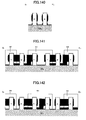
- the first embodiment shows a one-row-by-four-column CMOS inverter cascade circuit, wherein: a first inverter at an intersection of the 1st row and the 1st column in a one-row by four-column array is formed by arranging two p-channel MOS SGTs at respective ones of an intersection of the 1st row and the 1st column and an intersection of the 2nd row and the 1st column, and arranging one n-channel MOS SGT at an intersection of the 1st row and the 2nd column; a second inverter at an intersection of the 1 st row and the 2nd column in the one-row by four-column array is formed by arranging two p-channel MOS SGTs at respective ones of an intersection of the 1st row and the 3rd column and the intersection of the 2nd row and the 3rd column, and arranging one n-channel MOS SGT at an intersection of the 2nd row and the 2nd column; a third inverter at an
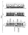
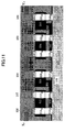
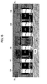
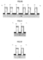
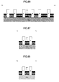
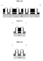
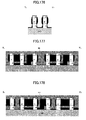
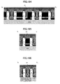
- FIG. 8 shows a CMOS inverter cascade circuit according to a second embodiment of the present invention, wherein the CMOS inverters are arranged in a three-row by four-column array.
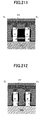
- FIG. 9 is a sectional view taken along the line X 1 -X' 1 in FIG. 8
- FIG. 10 is a sectional view taken along the line X 2 -X' 2 in FIG. 8
- FIG. 11 is a sectional view taken along the line X 3 -X' 3 in FIG. 11
- FIG. 12 is a sectional view taken along the line X 4 -X' 4 in FIG. 8
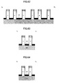
- FIG. 13 is a sectional view taken along the line X 5 -X' 5 in FIG. 8
- FIG. 14 is a sectional view taken along the line X 6 -X' 6 in FIG. 8
- FIG. 15 is a sectional view taken along the line Y 1 -Y' 1 in FIG. 8
- FIG. 16 is a sectional view taken along the line Y 2 -Y' 2 in FIG. 8 .
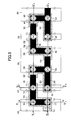
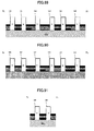
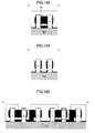
- one n-channel semiconductor device is arranged at an intersection of the 1st row and the 2nd column, wherein the n-channel semiconductor device comprises: an output terminal line 119 based on an island-shaped semiconductor lower layer (island-shaped semiconductor lower layer-based line 119), and a drain diffusion layer 109, each formed on a silicon oxide film 108 of a substrate; an island-shaped semiconductor layer 110 formed on the drain diffusion layer 109; a source diffusion layer 111 formed on top of the island-shaped semiconductor layer 110; and a gate 112 formed on a channel region of a sidewall of the island-shaped semiconductor layer 110 sandwiched between the drain diffusion layer 109 and the source diffusion layer 111, through a gate dielectric film.
- One of two p-channel semiconductor devices is arranged at an intersection of the 1st row and the 1st column, wherein the p-channel semiconductor device comprises: the island-shaped semiconductor lower layer-based line 119 and a drain diffusion layer 113 each formed on the silicon oxide film 108; an island-shaped semiconductor layer 114 formed on the drain diffusion layer 113; a source diffusion layer 115 formed on top of the island-shaped semiconductor layer 114; and the gate 112 formed on a channel region of a sidewall of the island-shaped semiconductor layer 114 sandwiched between the drain diffusion layer 113 and the source diffusion layer 115, through a gate dielectric film.
- the other p-channel semiconductor device is arranged at an intersection of the 2nd row and the 1st column, wherein the p-channel semiconductor device comprises: the island-shaped semiconductor lower layer-based line 119 and a drain diffusion layer 116 each formed on the silicon oxide film 108; an island-shaped semiconductor layer 117 formed on the drain diffusion layer 116; a source diffusion layer 118 formed on top of the island-shaped semiconductor layer 117; and the gate 112 formed on a channel region of a sidewall of the island-shaped semiconductor layer 117 sandwiched between the drain diffusion layer 116 and the source diffusion layer 118, through a gate dielectric film.
- the two p-channel semiconductor devices and the one n-channel semiconductor device make up an inverter at an intersection of the 1st row and the 1st column in the three-row by four-column array (1st-row/1st column inverter).
- one n-channel semiconductor device is arranged at an intersection of the 2nd row and the 2nd column, wherein the n-channel semiconductor device comprises: an output terminal line 130 based on an island-shaped semiconductor lower layer (island-shaped semiconductor lower layer-based line 130), and a drain diffusion layer 120, each formed on the silicon oxide film 108; an island-shaped semiconductor layer 121 formed on the drain diffusion layer 120; a source diffusion layer 122 formed on top of the island-shaped semiconductor layer 121; and a gate 123 formed on a channel region of a sidewall of the island-shaped semiconductor layer 121 sandwiched between the drain diffusion layer 120 and the source diffusion layer 122, through a gate dielectric film.
- One of two p-channel semiconductor devices is arranged at an intersection of the 1st row and the 3rd column, wherein the p-channel semiconductor device comprises: the island-shaped semiconductor lower layer-based line 130 and a drain diffusion layer 127 each formed on the silicon oxide film 108; an island-shaped semiconductor layer 128 formed on the drain diffusion layer 127; a source diffusion layer 129 formed on top of the island-shaped semiconductor layer 128; and the gate 123 formed on to a channel region of a sidewall of the island-shaped semiconductor layer 128 sandwiched between the drain diffusion layer 127 and the source diffusion layer 129, through a gate dielectric film.
- the other p-channel semiconductor device is arranged at an intersection of the 2nd row and the 3rd column, wherein the p-channel semiconductor device comprises: the island-shaped semiconductor lower layer-based line 130 and a drain diffusion layer 124 each formed on the silicon oxide film 108; an island-shaped semiconductor layer 125 formed on the drain diffusion layer 124; a source diffusion layer 126 formed on top of the island-shaped semiconductor layer 125; and the gate 123 formed on a channel region of a sidewall of the island-shaped semiconductor layer 125 sandwiched between the drain diffusion layer 124 and the source diffusion layer 125, through a gate dielectric film.
- the two p-channel semiconductor devices and the one n-channel semiconductor device make up an inverter at an intersection of the 1st row and the 2nd column in the three-row by four-column array (1st-row/2nd-column inverter).
- one n-channel semiconductor device is arranged at an intersection of the 1st row and the 5th column, wherein the n-channel semiconductor device comprises: an output terminal line 141 based on an island-shaped semiconductor lower layer (island-shaped semiconductor lower layer-based line 141), and a drain diffusion layer 131, each formed on the silicon oxide film 108; an island-shaped semiconductor layer 132 formed on the drain diffusion layer 131; a source diffusion layer 133 formed on top of the island-shaped semiconductor layer 132; and a gate 134 formed on a channel region of a sidewall of the island-shaped semiconductor layer 132 sandwiched between the drain diffusion layer 131 and the source diffusion layer 133, through a gate dielectric film.
- the p-channel semiconductor device comprises: the island-shaped semiconductor lower layer-based line 141 and a drain diffusion layer 138, each formed on the silicon oxide film 108; an island-shaped semiconductor layer 139 formed on the drain diffusion layer 138; a source diffusion layer 140 formed on top of the island-shaped semiconductor layer 139; and the gate 134 formed on a channel region of a sidewall of the island-shaped semiconductor layer 139 sandwiched between the drain diffusion layer 138 and the source diffusion layer 140, through a gate dielectric film.
- the other p-channel semiconductor device is arranged at an intersection of the 2nd row and the 4th column, wherein p-channel semiconductor device comprises: the island-shaped semiconductor lower layer-based line 141 and a drain diffusion layer 135 each formed on the silicon oxide film 108; an island-shaped semiconductor layer 136 formed on the drain diffusion layer 135; a source diffusion layer 137 formed on top of the island-shaped semiconductor layer 136; and the gate 134 formed on a channel region of a sidewall of the island-shaped semiconductor layer 136 sandwiched between the drain diffusion layer 135 and the source diffusion layer 137, through a gate dielectric film.
- the two p-channel semiconductor devices and the one n-channel semiconductor device make up an inverter at an intersection of the 1st row and the 3rd column in the three-row by four-column array (1st-row/3rd-column inverter).
- one n-channel semiconductor device is arranged at an intersection of the 2nd row and the 5th column, wherein the n-channel semiconductor device comprises: an output terminal line 152 based on an island-shaped semiconductor lower layer (island-shaped semiconductor lower layer-based line 152), and a drain diffusion layer 142, each formed on the silicon oxide film 108; an island-shaped semiconductor layer 143 formed on the drain diffusion layer 142; a source diffusion layer 144 formed on top of the island-shaped semiconductor layer 143; and a gate 145 formed on a channel region of a sidewall of the island-shaped semiconductor layer 143 sandwiched between the drain diffusion layer 142 and the source diffusion layer 144, through a gate dielectric film.
- One of two p-channel semiconductor device is arranged at an intersection of the 1st row and the 6th column, wherein the p-channel semiconductor device comprises: the island-shaped semiconductor lower layer-based line 152 and a drain diffusion layer 149 each formed on the silicon oxide film 108; an island-shaped semiconductor layer 150 formed on the drain diffusion layer 149; a source diffusion layer 151 formed on top of the island-shaped semiconductor layer 150; and the gate 145 formed on a channel region of a sidewall of the island-shaped semiconductor layer 150 sandwiched between the drain diffusion layer 149 and the source diffusion layer 151, through a gate dielectric film.
- the other p-channel semiconductor device is arranged at an intersection of the 2nd row and the 6th column, wherein the p-channel semiconductor device comprises: the island-shaped semiconductor lower layer-based line 152 and a drain diffusion layer 146 each formed on the silicon oxide film 108; an island-shaped semiconductor layer 147 formed on the drain diffusion layer 146; a source diffusion layer 148 formed on top of the island-shaped semiconductor layer 147; and the gate 145 formed on a channel region of a sidewall of the island-shaped semiconductor layer 147 sandwiched between the drain diffusion layer 146 and the source diffusion layer 148, through a gate dielectric film.
- the two p-channel semiconductor devices and the one n-channel semiconductor device make up an inverter at an intersection of the 1st row and the 4th column in the three-row by four-column array (1st-row/4th-column inverter).
- a first power supply line Vssl 157 as a Vss line is formed on the source diffusion layers 111, 122 of the two n-channel semiconductor devices of the 1st-row/1st-column and 1st-row/2nd-column inverters, and a first power supply line Vssl 159 as a Vss line is formed on the source diffusion layers 133, 144 of the two n-channel semiconductor devices of the 1st-row/3rd-column and 1st-row/4th-column inverters.
- a second power supply line Vccl 156 as a Vcc line is formed on the source diffusion layers 115, 118 of the two p-channel semiconductor devices of the 1st-row/1st-column inverter.
- a second power supply line Vccl 158 as a Vcc line is formed on the source diffusion layers 129, 126, 140, 137 of the four p-channel semiconductor devices of the 1st-row/2nd-column and 1st-row/3rd-column inverters, and a second power supply line Vccl 160 as a Vcc line is formed on the source diffusion layers 148, 151 of the two p-channel semiconductor devices of the 1st-row/4th-column inverter.
- the gate 112 serves as an input terminal line of the 1st-row/1st-column inverter.
- the gate 123 serves as an input terminal line of the 1st-row/2nd-column inverter.
- the gate 134 serves as an input terminal line of the 1st-row/3rd-column inverter.
- the gate 145 serves as an input terminal line of the 1st-row/4th-column inverter.
- a contact 153 is formed to connect the gate 123 and the island-shaped semiconductor lower layer-based output terminal line 119 of the 1st-row/1st-column inverter.
- a contact 154 is formed to connect the gate 134 and the island-shaped semiconductor lower layer-based output terminal line 130 of the 1st-row/2nd-column inverter.
- a contact 155 is formed to connect the gate 145 and the island-shaped semiconductor lower layer-based output terminal line 141 of the 1st-row/3rd-column inverter.
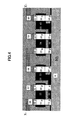
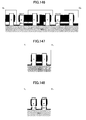
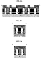
- one n-channel semiconductor device is arranged at an intersection of the 3rd row and the 2nd column, wherein the n-channel semiconductor device comprises: an output terminal line 219 based on an island-shaped semiconductor lower layer (island-shaped semiconductor lower layer-based line 219), and a drain diffusion layer 209, each formed on the silicon oxide film 108; an island-shaped semiconductor layer 210 formed on the drain diffusion layer 209; a source diffusion layer 211 formed on top of the island-shaped semiconductor layer 210; and a gate 212 formed on a channel region of a sidewall of the island-shaped semiconductor layer 210 sandwiched between the drain diffusion layer 209 and the source diffusion layer 211, through a gate dielectric film.
- the p-channel semiconductor device comprises: the island-shaped semiconductor lower layer-based line 219 and a drain diffusion layer 213 each formed on the silicon oxide film 108; an island-shaped semiconductor layer 214 formed on the drain diffusion layer 213; a source diffusion layer 215 formed on top of the island-shaped semiconductor layer 214; and the gate 212 formed on a channel region of a sidewall of the island-shaped semiconductor layer 214 sandwiched between the drain diffusion layer 213 and the source diffusion layer 215, through a gate dielectric film.
- the other p-channel semiconductor device is arranged at an intersection of the fourth row and the 1st column, wherein the p-channel semiconductor device comprises: the island-shaped semiconductor lower layer-based line 219 and a drain diffusion layer 216 each formed on the silicon oxide film 108; an island-shaped semiconductor layer 217 formed on the drain diffusion layer 216; a source diffusion layer 218 formed on top of the island-shaped semiconductor layer 217; and the gate 212 formed on a channel region of a sidewall of the island-shaped semiconductor layer 217 sandwiched between the drain diffusion layer 216 and the source diffusion layer 218, through a gate dielectric film.
- the two p-channel semiconductor devices and the one n-channel semiconductor device make up an inverter at an intersection of the 2nd row and the 1st column in the three-row by four-column array (2nd-row/1st-column inverter).
- one n-channel semiconductor device is arranged at an intersection of the 4th row and the 2nd column, wherein the n-channel semiconductor device comprises: an output terminal line 230 based on an island-shaped semiconductor lower layer (island-shaped semiconductor lower layer-based line 230), and a drain diffusion layer 220, each formed on the silicon oxide film 108; an island-shaped semiconductor layer 221 formed on the drain diffusion layer 220; a source diffusion layer 222 formed on top of the island-shaped semiconductor layer 221; and a gate 223 formed on a channel region of a sidewall of the island-shaped semiconductor layer 221 sandwiched between the drain diffusion layer 220 and the source diffusion layer 222, through a gate dielectric film.
- One of two p-channel semiconductor devices is at an intersection of the 3rd row and the 3rd column, wherein the p-channel semiconductor device comprises: the island-shaped semiconductor lower layer-based line 230 and a drain diffusion layer 227 each formed on the silicon oxide film 108; an island-shaped semiconductor layer 228 formed on the drain diffusion layer 227; a source diffusion layer 229 formed on top of the island-shaped semiconductor layer 228; and the gate 223 formed on to a channel region of a sidewall of the island-shaped semiconductor layer 228 sandwiched between the drain diffusion layer 227 and the source diffusion layer 229, through a gate dielectric film.
- the other p-channel semiconductor device is arranged at an intersection of the 4th row and the 3rd column, wherein the p-channel semiconductor device comprises: the island-shaped semiconductor lower layer-based line 230 and a drain diffusion layer 224 each formed on the silicon oxide film 108; an island-shaped semiconductor layer 225 formed on the drain diffusion layer 224; a source diffusion layer 226 formed on top of the island-shaped semiconductor layer 225; and the gate 223 formed on a channel region of a sidewall of the island-shaped semiconductor layer 225 sandwiched between the drain diffusion layer 224 and the source diffusion layer 225, through a gate dielectric film.
- the two p-channel semiconductor devices and the one n-channel semiconductor device make up an inverter at an intersection of the 2nd row and the 2nd column in the three-row by four-column array (2nd-row/2nd-column inverter).
- one n-channel semiconductor device is arranged at an intersection of the 3rd row and the 5th column, wherein the n-channel semiconductor device comprises: an output terminal line 241 based on an island-shaped semiconductor lower layer (island-shaped semiconductor lower layer-based line 241), and a drain diffusion layer 231, each formed on the silicon oxide film 108; an island-shaped semiconductor layer 232 formed on the drain diffusion layer 231; a source diffusion layer 233 formed on top of the island-shaped semiconductor layer 232; and a gate 234 formed on a channel region of a sidewall of the island-shaped semiconductor layer 232 sandwiched between the drain diffusion layer 231 and the source diffusion layer 233, through a gate dielectric film.
- the p-channel semiconductor device comprises: the island-shaped semiconductor lower layer-based line 241 and a drain diffusion layer 238 each formed on the silicon oxide film 108; an island-shaped semiconductor layer 239 formed on the drain diffusion layer 238; a source diffusion layer 240 formed on top of the island-shaped semiconductor layer 239; and the gate 234 formed on a channel region of a sidewall of the island-shaped semiconductor layer 239 sandwiched between the drain diffusion layer 238 and the source diffusion layer 240, through a gate dielectric film.
- the other p-channel semiconductor device is arranged at an intersection of the 4th row and the 4th column, wherein the p-channel semiconductor device comprises: the island-shaped semiconductor lower layer-based line 241 and a drain diffusion layer 235 each formed on the silicon oxide film 108; an island-shaped semiconductor layer 236 formed on the drain diffusion layer 235; a source diffusion layer 237 formed on top of the island-shaped semiconductor layer 236; and the gate 234 formed on a channel region of a sidewall of the island-shaped semiconductor layer 236 sandwiched between the drain diffusion layer 235 and the source diffusion layer 237, through a gate dielectric film.
- the two p-channel semiconductor devices and the one n-channel semiconductor device make up an inverter at an intersection of the 2nd row and the 3rd column in the three-row by four-column array (2nd-row/3rd-column inverter).
- one n-channel semiconductor device is arranged at an intersection of the 4th row and the 5th column, wherein the n-channel semiconductor device comprises: an output terminal line 252 based on an island-shaped semiconductor lower layer (island-shaped semiconductor lower layer-based line 252), and a drain diffusion layer 242, each formed on the silicon oxide film 108; an island-shaped semiconductor layer 243 formed on the drain diffusion layer 242; a source diffusion layer 244 formed on top of the island-shaped semiconductor layer 243; and a gate 245 formed on a channel region of a sidewall of the island-shaped semiconductor layer 243 sandwiched between the drain diffusion layer 242 and the source diffusion layer 244, through a gate dielectric film.
- the n-channel semiconductor device comprises: an output terminal line 252 based on an island-shaped semiconductor lower layer (island-shaped semiconductor lower layer-based line 252), and a drain diffusion layer 242, each formed on the silicon oxide film 108; an island-shaped semiconductor layer 243 formed on the drain diffusion layer 242; a source diffusion layer
- the p-channel semiconductor device comprises: the island-shaped semiconductor lower layer-based line 252 and a drain diffusion layer 249 each formed on the silicon oxide film 108; an island-shaped semiconductor layer 250 formed on the drain diffusion layer 249; a source diffusion layer 251 formed on top of the island-shaped semiconductor layer 250; and the gate 245 formed on a channel region of a sidewall of the island-shaped semiconductor layer 250 sandwiched between the drain diffusion layer 249 and the source diffusion layer 251, through a gate dielectric film.
- the other p-channel semiconductor device is arranged at an intersection of the 4th row and the 6th column, wherein the p-channel semiconductor device comprises: the island-shaped semiconductor lower layer-based line 252 and a drain diffusion layer 246 each formed on the silicon oxide film 108; an island-shaped semiconductor layer 247 formed on the drain diffusion layer 246; a source diffusion layer 248 formed on top of the island-shaped semiconductor layer 247; and the gate 245 formed on a channel region of a sidewall of the island-shaped semiconductor layer 247 sandwiched between the drain diffusion layer 246 and the source diffusion layer 248, through a gate dielectric film.
- the two p-channel semiconductor devices and the one n-channel semiconductor device make up an inverter at an intersection of the 2nd row and the 4th column in the three-row by four-column array (2nd-row/4th-column inverter).
- the first power supply line Vssl 157 is formed on the source diffusion layers 211, 222 of the two n-channel semiconductor devices of the 2nd-row/1st-column and 2nd-row/2nd-column inverters, and the first power supply line Vssl 159 is formed on the source diffusion layers 233, 244 of the two n-channel semiconductor devices of the 2nd-row/3rd-column and 2nd-row/4th-column inverters. Further, the second power supply line Vccl 156 is formed on the source diffusion layers 215, 218 of the two p-channel semiconductor devices of the 2nd-row/1st-column inverter.
- the second power supply line Vccl 158 is formed on the source diffusion layers 229, 226, 240, 237 of the four p-channel semiconductor devices of the 2nd-row/2nd-column and 2nd-row/3rd-column inverters, and the second power supply line Vccl 160 is formed on the source diffusion layers 248, 251 of the two p-channel semiconductor devices of the 2nd-row/4th-column inverter.
- the gate 212 serves as an input terminal line of the 2nd-row/1st-column inverter.
- the gate 223 serves as an input terminal line of the 2nd-row/2nd-column inverter.
- the gate 234 serves as an input terminal line of the 2nd-row/3rd-column inverter.
- the gate 245 serves as an input terminal line of the 2nd-row/4th-column inverter.
- a contact 253 is formed to connect the gate 223 and the island-shaped semiconductor lower layer-based output terminal line 219 of the 2nd-row/1st-column inverter.
- a contact 254 is formed to connect the gate 234 and the island-shaped semiconductor lower layer-based output terminal line 230 of the 2nd-row/2nd-column inverter.
- a contact 255 is formed to connect the gate 245 and the island-shaped semiconductor lower layer-based output terminal line 241 of the 2nd-row/3rd-column inverter.
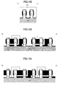
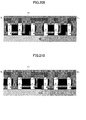
- one n-channel semiconductor device is arranged at an intersection of the 5th row and the 2nd column, wherein the n-channel semiconductor device comprises: an output terminal line 319 based on an island-shaped semiconductor lower layer (island-shaped semiconductor lower layer-based line 319), and a drain diffusion layer 309, each formed on the silicon oxide film 108; an island-shaped semiconductor layer 310 formed on the drain diffusion layer 309; a source diffusion layer 311 formed on top of the island-shaped semiconductor layer 310; and a gate 312 formed on a channel region of a sidewall of the island-shaped semiconductor layer 310 sandwiched between the drain diffusion layer 309 and the source diffusion layer 311, through a gate dielectric film.
- One of two p-channel semiconductor devices is arranged at an intersection of the 5th row and the 1st column, wherein the p-channel semiconductor device comprises: the island-shaped semiconductor lower layer-based line 319 and a drain diffusion layer 313 each formed on the silicon oxide film 108; an island-shaped semiconductor layer 314 formed on the drain diffusion layer 313; a source diffusion layer 31 formed on top of the island-shaped semiconductor layer 314; and the gate 312 formed on a channel region of a sidewall of the island-shaped semiconductor layer 314 sandwiched between the drain diffusion layer 313 and the source diffusion layer 315, through a gate dielectric film.
- the other p-channel semiconductor device is arranged at an intersection of the 6th row and the 1st column, wherein the p-channel semiconductor device comprises: the island-shaped semiconductor lower layer-based line 319 and a drain diffusion layer 316 each formed on the silicon oxide film 108; an island-shaped semiconductor layer 317 formed on the drain diffusion layer 316; a source diffusion layer 318 formed on top of the island-shaped semiconductor layer 317; and the gate 312 formed on a channel region of a sidewall of the island-shaped semiconductor layer 317 sandwiched between the drain diffusion layer 316 and the source diffusion layer 318, through a gate dielectric film.
- the two p-channel semiconductor devices and the one n-channel semiconductor device make up an inverter at an intersection of the 3rd row and the 1st column in the three-row by four-column array (3rd-row/1st-column inverter).
- one n-channel semiconductor device is arranged at an intersection of the 6th row and the 2nd column, wherein the n-channel semiconductor device comprises: an output terminal line 330 based on an island-shaped semiconductor lower layer (island-shaped semiconductor lower layer-based line 330), and a drain diffusion layer 320, each formed on the silicon oxide film 108; an island-shaped semiconductor layer 321 formed on the drain diffusion layer 320; a source diffusion layer 322 formed on top of the island-shaped semiconductor layer 321; and a gate 323 formed on a channel region of a sidewall of the island-shaped semiconductor layer 321 sandwiched between the drain diffusion layer 320 and the source diffusion layer 322, through a gate dielectric film.
- One of two p-channel semiconductor devices is arranged at an intersection of the 5th row and the 3rd column, wherein the p-channel semiconductor device comprises: the island-shaped semiconductor lower layer-based line 330 and a drain diffusion layer 327 each formed on the silicon oxide film 108; an island-shaped semiconductor layer 328 formed on the drain diffusion layer 327; a source diffusion layer 329 formed on top of the island-shaped semiconductor layer 328; and the gate 323 formed on to a channel region of a sidewall of the island-shaped semiconductor layer 328 sandwiched between the drain diffusion layer 327 and the source diffusion layer 329, through a gate dielectric film.
- the other p-channel semiconductor device is arranged at an intersection of the 6th row and the 3rd column, wherein the p-channel semiconductor device comprises: the island-shaped semiconductor lower layer-based line 330 and a drain diffusion layer 324 each formed on the silicon oxide film 108; an island-shaped semiconductor layer 325 formed on the drain diffusion layer 324; a source diffusion layer 326 formed on top of the island-shaped semiconductor layer 325; and the gate 323 formed on a channel region of a sidewall of the island-shaped semiconductor layer 325 sandwiched between the drain diffusion layer 324 and the source diffusion layer 325, through a gate dielectric film.
- the two p-channel semiconductor devices and the one n-channel semiconductor device make up an inverter at an intersection of the 3rd row and the 2nd column in the three-row by four-column array (3rd-row/2nd-column inverter).
- one n-channel semiconductor device is arranged at an intersection of the 5th row and the 5th column, wherein the n-channel semiconductor device comprises: an output terminal line 341 based on an island-shaped semiconductor lower layer (island-shaped semiconductor lower layer-based line 341), and a drain diffusion layer 331, each formed on the silicon oxide film 108; an island-shaped semiconductor layer 332 formed on the drain diffusion layer 331; a source diffusion layer 333 formed on top of the island-shaped semiconductor layer 332; and a gate 334 formed on a channel region of a sidewall of the island-shaped semiconductor layer 332 sandwiched between the drain diffusion layer 331 and the source diffusion layer 333, through a gate dielectric film.
- the n-channel semiconductor device comprises: an output terminal line 341 based on an island-shaped semiconductor lower layer (island-shaped semiconductor lower layer-based line 341), and a drain diffusion layer 331, each formed on the silicon oxide film 108; an island-shaped semiconductor layer 332 formed on the drain diffusion layer 331; a source diffusion
- One of two p-channel semiconductor devices is arranged at an intersection of the 5th row and the 4th column, wherein the p-channel semiconductor device comprises: the island-shaped semiconductor lower layer-based line 341 and a drain diffusion layer 338 each formed on the silicon oxide film 108; an island-shaped semiconductor layer 339 formed on the drain diffusion layer 338; a source diffusion layer 340 formed on top of the island-shaped semiconductor layer 339; and the gate 334 formed on to a channel region of a sidewall of the island-shaped semiconductor layer 339 sandwiched between the drain diffusion layer 338 and the source diffusion layer 340, through a gate dielectric film.
- the other p-channel semiconductor device is arranged at an intersection of the 6th row and the 4th column, wherein the p-channel semiconductor device comprises: the island-shaped semiconductor lower layer-based line 341 and a drain diffusion layer 335 each formed on the silicon oxide film 108; an island-shaped semiconductor layer 336 formed on the drain diffusion layer 335; a source diffusion layer 337 formed on top of the island-shaped semiconductor layer 336; and the gate 334 formed on a channel region of a sidewall of the island-shaped semiconductor layer 336 sandwiched between the drain diffusion layer 335 and the source diffusion layer 337, through a gate dielectric film.
- the two p-channel semiconductor devices and the one n-channel semiconductor device make up an inverter at an intersection of the 3rd row and the 3rd column in the three-row by four-column array (3rd-row/3rd-column inverter).
- one n-channel semiconductor device is arranged at an intersection of the 6th row and the 5th column, wherein the n-channel semiconductor device comprises: an output terminal line 352 based on an island-shaped semiconductor lower layer (island-shaped semiconductor lower layer-based line 352), and a drain diffusion layer 342, each formed on the silicon oxide film 108; an island-shaped semiconductor layer 343 formed on the drain diffusion layer 342; a source diffusion layer 344 formed on top of the island-shaped semiconductor layer 343; and a gate 345 formed on a channel region of a sidewall of the island-shaped semiconductor layer 343 sandwiched between the drain diffusion layer 342 and the source diffusion layer 344, through a gate dielectric film.
- One of two p-channel semiconductor devices is arranged at an intersection of the 5th row and the 6th column, wherein the p-channel semiconductor device comprises: the island-shaped semiconductor lower layer-based line 352 and a drain diffusion layer 349 each formed on the silicon oxide film 108; an island-shaped semiconductor layer 350 formed on the drain diffusion layer 349; a source diffusion layer 351 formed on top of the island-shaped semiconductor layer 350; and the gate 345 formed on a channel region of a sidewall of the island-shaped semiconductor layer 350 sandwiched between the drain diffusion layer 349 and the source diffusion layer 351, through a gate dielectric film.
- the other p-channel semiconductor device is arranged at an intersection of the 6th row and the 6th column, wherein the p-channel semiconductor device comprises: the island-shaped semiconductor lower layer-based line 352 and a drain diffusion layer 346 each formed on the silicon oxide film 108; an island-shaped semiconductor layer 347 formed on the drain diffusion layer 346; a source diffusion layer 348 formed on top of the island-shaped semiconductor layer 347; and the gate 345 formed on a channel region of a sidewall of the island-shaped semiconductor layer 347 sandwiched between the drain diffusion layer 346 and the source diffusion layer 348, through a gate dielectric film.
- the two p-channel semiconductor devices and the one n-channel semiconductor device make up an inverter at an intersection of the 3rd row and the 4th column in the three-row by four-column array (3rd-row/4th-column inverter).
- the first power supply line Vssl 157 is formed on the source diffusion layers 311, 322 of the two n-channel semiconductor devices of the 3rd-row/1st-column and 3rd-row/2nd-column inverters, and the first power supply line Vssl 159 is formed on the source diffusion layers 333, 344 of the two n-channel semiconductor devices of the 3rd-row/3rd-column and 3rd-row/4th-column inverters. Further, the second power supply line Vccl 156 is formed on the source diffusion layers 315, 318 of the two p-channel semiconductor devices of the 3rd-row/1st-column inverter.
- the second power supply line Vccl 158 is formed on the source diffusion layers 329, 326, 340, 337 of the four p-channel semiconductor devices of the 3rd-row/2nd-column and 3rd-row/3rd-column inverters, and the second power supply line Vccl 160 is formed on the source diffusion layers 348, 351 of the two p-channel semiconductor devices of the 3rd-row/4th-column inverter.
- the gate 312 serves as an input terminal line of the 3rd-row/1st-column inverter.
- the gate 323 serves as an input terminal line of the 3rd-row/2nd-column inverter.
- the gate 334 serves as an input terminal line of the 3rd-row/3rd-column inverter.
- the gate 345 serves as an input terminal line of the 3rd-row/4th-column inverter.
- a contact 353 is formed to connect the gate 323 and the island-shaped semiconductor lower layer-based output terminal line 319 of the 3rd-row/1st-column inverter.
- a contact 354 is formed to connect the gate 334 and the island-shaped semiconductor lower layer-based output terminal line 330 of the 3rd-row/2nd-column inverter.
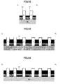
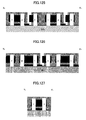
- FIG. 17 is a diagram showing a silicon-on-insulator (SOI) substrate, in X 1 -X' 1 section, wherein a silicon layer 500 is formed on a silicon oxide film, and a silicon oxide film 501 is formed by oxidizing a surface of the silicon layer 500.
- SOI silicon-on-insulator
- FIGS. 17 to 20 illustrate the SOI substrate in X 2 -X' 2 section, Y 1 -Y' 1 section and Y 2 -Y' 2 , respectively.
- the X 1 -X' 1 section, the X 2 -X' 2 section, the Y 1 -Y' 1 section, and the Y 2 -Y' 2 section correspond to FIG. 4 , FIG. 5 , FIG. 6, and FIG. 7 , respectively.
- the silicon layer 500 is etched by reactive ion etching using a resist as a mask to form a required number of silicon pillars. Subsequently, surfaces of the silicon pillars are oxidized, and then resists 502, 503, 504 are formed to allow a part of the silicon pillars to be formed as p-type silicon pillars ( FIG. 21 (X 1 -X' 1 ), FIG. 22 (X 2 -X' 2 ), FIG. 23 (Y 1 -Y' 1 ) and FIG. 24 (Y 2 -Y' 2 )).
- Boron (B) is implanted into the unmasked silicon pillars by an ion-implantation process or the like, to form p-type silicon pillars 505, 506, 507, 508 ( FIG. 25 (X 1 -X' 1 ), FIG. 26 (X 2 -X' 2 ), FIG. 27 (Y 1 -Y' 1 ) and FIG. 28 (Y 2 -Y' 2 )).
- resists 509, 510 are formed to allow the remaining silicon pillars to be formed as n-type silicon pillars ( FIG. 29 (X 1 -X' 1 ), FIG. 30 (X 2 -X' 2 ), FIG. 31 (Y 1 -Y' 1 ) and FIG. 32 (Y 2 -Y' 2 )).
- Phosphorus (P) is implanted into the unmasked silicon pillars by an ion-implantation process or the like, to form n-type silicon pillars 511, 512, 513, 514, 515, 516, 517, 518 ( FIG. 33 (X 1 -X' 1 ), FIG. 34 (X 2 -X' 2 ), FIG. 35 (Y 1 -Y' 1 ) and FIG. 36 (Y 2 -Y' 2 )).
- the silicon pillars are subjected to a thermal process to ionize the impurity ( FIG. 37 (X 1 -X' 1 ), FIG. 38 (X 2 -X' 2 ), FIG. 39 (Y 1 -Y' 1 ) and FIG 40 (Y 2 -Y' 2 )).
- a nitride film 519 is deposited, and flattened by chemical mechanical polishing (CMP). Then, the nitride film 519 is etched back ( FIG. 41 (X 1 -X' 1 ), FIG. 42 (X 2 -X' 2 ), FIG. 43 (Y 1 -Y' 1 ) and FIG. 44 (Y 2 -Y' 2 )).
- a polysilicon film 520 is deposited, and flattened by CMP. Then, the polysilicon film 520 is etched back ( FIG. 45 (X 1 -X' 1 ), FIG. 46 (X 2 -X' 2 ), FIG. 47 (Y 1 -Y' 1 ) and FIG. 48 (Y 2 -Y' 2 )).
- a nitride film is deposited in such a manner that it remains on a sidewall of each of the island-shaped semiconductor sections, in the form of a sidewall spacer ( FIG. 49 (X 1 -X' 1 ), FIG. 50 (X 2 -X' 2 ), FIG. 51 (Y 1 -Y' 1 ) and FIG. 52 (Y 2 -Y' 2 )).
- the polysilicon film is etched away ( FIG. 53 (X 1 -X' 1 ), FIG. 54 (X 2 -X' 2 ), FIG. 55 (Y 1 -Y' 1 ) and FIG. 56 (Y 2 -Y' 2 )).
- the exposed oxide film on each of the island-shaped semiconductor sections is etched away ( FIG. 57 (X 1 -X' 1 ), FIG. 58 (X 2 -X' 2 ), FIG. 59 (Y 1 -Y' 1 ) and FIG. 60 (Y 2 -Y' 2 )).
- a polysilicon film 533 is deposited, and flattened by CMP. Then, the polysilicon film 533 is etched back ( FIG. 61 (X 1 -X' 1 ), FIG. 62 (X 2 -X' 2 ), FIG. 63 (Y 1 -Y' 1 ) and FIG. 64 (Y 2 -Y' 2 )).
- the nitride film is etched away ( FIG. 65 (X 1 -X' 1 ), FIG. 66 (X 2 -X' 2 ), FIG. 67 (Y 1 -Y' 1 ) and FIG. 68 (Y 2 -Y' 2 )).
- Resists 534, 535, 536, 537 are formed to allow an island-shaped semiconductor lower layer-based output terminal line to be formed ( FIG. 69 (X 1 -X' 1 ), FIG. 70 (X 2 -X' 2 ), FIG. 71 (Y 1 -Y' 1 ) and FIG. 72 (Y 2 -Y' 2 )).
- the polysilicon film is etched to form island-shaped semiconductor lower layer-based output terminal lines 19, 30, 41, 52 ( FIG. 73 (X 1 -X' 1 ), FIG. 74 (X 2 -X' 2 ), FIG. 75 (Y 1 -Y' 1 ) and FIG. 76 (Y 2 -Y' 2 )).
- FIG. 77 (X 1 -X' 1 ), FIG. 78 (X 2 -X' 2 ), FIG. 79 (Y 1 -Y' 1 ) and FIG. 80 (Y 2 -Y' 2 )).
- An oxide film 538 is deposited, and flattened by CMP. Then, the oxide film 538 is etched back ( FIG. 81 (X 1 -X' 1 ), FIG. 82 (X 2 -X' 2 ), FIG. 83 (Y 1 -Y' 1 ) and FIG. 84 (Y 2 -Y' 2 )).
- a nitride film 539 is deposited, and flattened by CMP. Then, the nitride film 539 is etched back ( FIG. 85 (X 1 -X' 1 ), FIG. 86 (X 2 -X' 2 ), FIG. 87 (Y 1 -Y' 1 ) and FIG. 88 (Y 2 -Y' 2 )).
- the island-shaped semiconductor layers are surface-oxidized to form gate dielectric films 540, 541, 542, 543, 544, 545, 546, 547, 548, 549, 550, 551 thereon ( FIG. 89 (X 1 -X' 1 ), FIG. 90 (X 2 -X' 2 ), FIG. 91 (Y 1 -Y' 1 ) and FIG. 92 (Y 2 -Y' 2 )).
- a polysilicon film 552 is deposited, and flattened by CMP. Then, the polysilicon film 552 is etched back ( FIG. 93 (X 1 -X' 1 ), FIG. 94 (X 2 -X' 2 ), FIG. 95 (Y 1 -Y' 1 ) and FIG. 96 (Y 2 -Y' 2 )).
- a nitride film 553 is deposited, and flattened by CMP. Then, the nitride film 553 is etched back ( FIG. 97 (X 1 -X' 1 ), FIG. 98 (X 2 -X' 2 ), FIG. 99 (Y 1 -Y' 1 ) and FIG. 100 (Y 2 -Y' 2 )).
- Resists 554, 555, 556, 557 are formed to allow an input terminal line to be formed ( FIG. 101 (X 1 -X' 1 ), FIG. 102 (X 2 -X' 2 ), FIG. 103 (Y 1 -Y' 1 ) and FIG. 104 (Y 2 -Y' 2 )).
- the nitride film 553, the polysilicon film 552 and nitride film 539 are etched to form input terminal lines or gates 12, 23, 34, 45 ( FIG. 105 (X 1 -X' 1 ), FIG. 106 (X 2 -X' 2 ), FIG. 107 (Y 1 -Y' 1 ) and FIG. 108 (Y 2 -Y' 2 )).
- FIG. 109 (X 1 -X' 1 ), FIG. 110 (X 2 -X' 2 ), FIG. 111 (Y 1 -Y' 1 ) and FIG. 112 (Y 2 -Y' 2 )).
- An oxide film 558 is deposited, and flattened by CMP. Then, the oxide film 558 is etched back ( FIG. 113 (X 1 -X' 1 ), FIG 114 (X 2 -X' 2 ), FIG. 115 (Y 1 -Y' 1 ) and FIG. 116 (Y 2 -Y' 2 )).
- a resist 559 is formed to allow contacts between respective ones of the gates and the island-shaped semiconductor lower layers ( FIG. 117 (X 1 -X' 1 ), FIG. 118 (X 2 -X' 2 ), FIG. 119 (Y 1 -Y' 1 ) and FIG. 120 (Y 2 -Y' 2 )).
- the oxide film is etched to form contact holes 560, 561, 562 between respective ones of the gates and the island-shaped semiconductor lower layers ( FIG. 121 (X 1 -X' 1 ), FIG. 122 (X 2 -X' 2 ), FIG. 123 (Y 1 -Y' 1 ) and FIG. 124 (Y 2 -Y' 2 )).
- the resist is removed ( FIG. 125 (X 1 -X' 1 ), FIG. 126 (X 2 -X' 2 ), FIG. 127 (Y 1 -Y' 1 ) and FIG. 128 (Y 2 -Y' 2 )).
- a polysilicon film is deposited, and flattened by CMP. Then, the polysilicon film is etched back to form contacts 53, 54, 55 between the respective ones of the gates and the island-shaped semiconductor lower layers ( FIG. 129 (X 1 -X' 1 ), FIG. 130 (X 2 -X' 2 ), FIG. 131 (Y 1 -Y' 1 ) and FIG. 132 (Y 2 -Y' 2 )).
- the oxide film is removed ( FIG. 133 (X 1 -X' 1 ), FIG. 134 (X 2 -X' 2 ), FIG. 135 (Y 1 -Y' 1 ) and FIG. 136 (Y 2 -Y' 2 )).
- a surface of each of the island-shaped semiconductor layers are oxidized ( FIG. 137 (X 1 -X' 1 ), FIG. 138 (X 2 -X' 2 ), FIG. 139 (Y 1 -Y' 1 ) and FIG. 140 (Y 2 -Y' 2 )).
- Resists 563, 564, 565 are formed to allow a drain diffusion layer and a source diffusion layer for an n-channel semiconductor device to be formed ( FIG. 141 (X 1 -X' 1 ), FIG. 142 (X 2 -X' 2 ), FIG. 143 (Y 1 -Y' 1 ) and FIG. 144 (Y 2 -Y' 2 )).
- Arsenic (As) is implanted into the p-type silicon pillars by an ion-implantation process or the like, to form drain diffusion layers 9, 20, 31, 42 and source diffusion layers 11, 22, 33, 44 therein ( FIG. 145 (X 1 -X' 1 ), FIG. 146 (X 2 -X' 2 ), FIG. 147 (Y 1 -Y' 1 ) and FIG. 148 (Y 2 -Y' 2 )).
- Resists 566, 567, 568 are formed to allow a drain diffusion layer and a source diffusion layer for a p-channel semiconductor device to be formed ( FIG. 149 (X 1 -X' 1 ), FIG. 150 (X 2 -X' 2 ), FIG. 151 (Y 1 -Y' 1 ) and FIG. 152 (Y 2 -Y' 2 )).
- Boron (B) is implanted into the n-type silicon pillars by an ion-implantation process or the like, to form drain diffusion layers 13, 16, 24, 27, 35, 38, 46, 49 and source diffusion layers 15, 18, 26, 29, 37, 40, 48, 51 therein ( FIG. 153 (X 1 -X' 1 ), FIG. 154 (X 2 -X' 2 ), FIG. 155 (Y 1 -Y' 1 ) and FIG. 156 (Y 2 -Y' 2 )).
- the silicon pillars are subjected to a thermal process to ionize the impurity ( FIG. 157 (X 1 -X' 1 ), FIG. 158 (X 2 -X' 2 ), FIG. 159 (Y 1 -Y' 1 ) and FIG. 160 (Y 2 -Y' 2 )).
- the oxide films are removed ( FIG. 161 (X 1 -X' 1 ), FIG. 162 (X 2 -X' 2 ), FIG. 163 (Y 1 -Y' 1 ) and FIG. 164 (Y 2 -Y' 2 )).
- a metal 568 such as cobalt (Co) or nickel (Ni), is deposited by sputtering or CVD ( FIG. 165 (X 1 -X' 1 ), FIG. 166 (X 2 -X' 2 ), FIG. 167 (Y 1 -Y' 1 ) and FIG. 168 (Y 2 -Y' 2 )).
- the resulting product is subjected to a thermal process so as to produce a reaction between the metal and silicon to form salicide ( FIG. 169 (X 1 -X' 1 ), FIG. 170 (X 2 -X' 2 ), FIG. 171 (Y 1 -Y' 1 ) and FIG. 172 (Y 2 -Y' 2 )).
- FIG. 173 (X 1 -X' 1 ), FIG. 174 (X 2 -X' 2 ), FIG. 175 (Y 1 -Y' 1 ) and FIG. 176 (Y 2 -Y' 2 )).
- An oxide film 569 is deposited, and flattened by CMP. Then, the oxide film 569 is etched back ( FIG. 177 (X 1 -X' 1 ), FIG. 178 (X 2 -X' 2 ), FIG. 179 (Y 1 -Y' 1 ) and FIG. 180 (Y 2 -Y' 2 )).
- a resist 570 is formed to allow a contact to be formed ( FIG. 181 (X 1 -X' 1 ), FIG. 182 (X 2 -X' 2 ), FIG. 183 (Y 1 -Y' 1 ) and FIG. 184 (Y 2 -Y' 2 )).
- the oxide film is etched ( FIG. 185 (X 1 -X' 1 ), FIG. 186 (X 2 -X' 2 ), FIG. 187 (Y 1 -Y' 1 ) and FIG. 188 (Y 2 -Y' 2 )).
- the resist is removed ( FIG. 189 (X 1 -X' 1 ), FIG. 190 (X 2 -X' 2 ), FIG. 191 (Y 1 -Y' 1 ) and FIG. 192 (Y 2 -Y' 2 )).
- a metal 571 is deposited, and flattened by CMP ( FIG. 193 (X 1 -X' 1 ), FIG. 194 (X 2 -X' 2 ), FIG. 195 (Y 1 -Y' 1 ) and FIG. 196 (Y 2 -Y' 2 )).
- Resists 572, 573, 574, 575, 576 are formed to allow a first power supply line and a second power supply line to be formed ( FIG. 197 (X 1 -X' 1 ), FIG. 198 (X 2 -X' 2 ), FIG. 199 (Y 1 -Y' 1 ) and FIG. 200 (Y 2 -Y' 2 )).
- the metal is etched to form first power supply lines Vssl 57, 59 as a Vss lines and form second power supply lines Vccl 56, 58, 60 as Vcc lines ( FIG. 201 (X 1 -X' 1 ), FIG. 202 (X 2 -X' 2 ), FIG. 203 (Y 1 -Y' 1 ) and FIG. 204 (Y 2 -Y' 2 )).
- FIG. 205 (X 1 -X' 1 ), FIG. 206 (X 2 -X' 2 ), FIG. 207 (Y 1 -Y' 1 ) and FIG. 208 (Y 2 -Y' 2 )).
- An oxide film 577 is deposited, and flattened by CMP ( FIG. 209 (X 1 -X' 1 ), FIG. 210 (X 2 -X' 2 ), FIG. 211 (Y 1 -Y' 1 ) and FIG. 212 (Y 2 -Y' 2 )).
- the conventional SGT-based two-stage CMOS inverter employs a structure where a first power supply potential Vss and a second power supply potential Vcc are supplied to respective diffusion layers in a silicon substrate SGTs through a plurality of contacts.
- two power supply lines for the nMOS and pMOS SGTs are arranged on one side of a lower portion of a gate region which is different from an on-substrate region where nMOS and pMOS layers are arranged.
- the semiconductor device comprises a first power supply line Vssl and a second power supply line Vccl each arranged to supply a respective one of a first power supply potential Vss and a second power supply potential Vcc to a corresponding one of an nMOS SGT and a pMOS SGT from thereabove, wherein: the first power supply line Vssl includes a first power supply line Vssl connected to a source diffusion layer of an n-channel semiconductor device in a first inverter, and a first power supply line Vssl connected to a source diffusion layer of an n-channel semiconductor device in a second inverter; and the second power supply line Vccl includes a second power supply line Vccl connected to respective source diffusion layers of two p-channel semiconductor devices in the first inverter, and a second power supply line Vccl connected to respective source diffusion layers of two p-channel semiconductor device in the second inverter.
- each of the first power supply line Vssl and the second power supply line Vccl is arranged to supply a respective one of a first power supply potential Vss and a second power supply potential Vcc to a corresponding one of an nMOS SGT and a pMOS SGT from thereabove, wherein: the first power supply line Vssl includes a first power supply line Vssl connected to a source diffusion layer of an n-channel semiconductor device in a first inverter, and a first power supply line Vssl connected to a source diffusion layer of an n-channel semiconductor device in a second inverter; and the second power supply line Vccl includes a second power supply line Vccl connected to respective source diffusion layers of two p-channel semiconductor devices in the first inverter, and a second power supply line Vccl connected to respective source diffusion layers of two p-channel semiconductor device in the second inverter, makes it possible reduce a resistance of the first power supply line Vs
- the semiconductor device comprises an output terminal arranged to interconnect the drain diffusion layer of the n-channel semiconductor device and the drain diffusion layers of the p-channel semiconductor devices, through an island-shaped semiconductor lower layer.
- the two p-MOS SGTs of the first inverter are arranged at respective ones of the intersection of the 1st row and the 1st column and the intersection of the 2nd row and the 1st column, and the n-MOS SGT of the first inverter is arranged at the intersection of the 1st row and the 2nd column.
- the two p-MOS SGTs of the second inverter are arranged at respective ones of the intersection of the 1st row and the 3rd column and the intersection of the 2nd row and the 3rd column, and the n-MOS SGT of the second inverter is arranged at the intersection of the 2nd row and the 2nd column.
Landscapes
- Metal-Oxide And Bipolar Metal-Oxide Semiconductor Integrated Circuits (AREA)
- Thin Film Transistor (AREA)
- Semiconductor Integrated Circuits (AREA)
Applications Claiming Priority (2)
| Application Number | Priority Date | Filing Date | Title |
|---|---|---|---|
| JP2007201687A JP5122212B2 (ja) | 2007-08-02 | 2007-08-02 | 半導体装置 |
| PCT/JP2008/059731 WO2009016880A1 (ja) | 2007-08-02 | 2008-05-27 | 半導体装置 |
Publications (3)
| Publication Number | Publication Date |
|---|---|
| EP2175489A1 true EP2175489A1 (de) | 2010-04-14 |
| EP2175489A4 EP2175489A4 (de) | 2012-08-22 |
| EP2175489B1 EP2175489B1 (de) | 2013-07-24 |
Family
ID=40304119
Family Applications (1)
| Application Number | Title | Priority Date | Filing Date |
|---|---|---|---|
| EP08764759.0A Not-in-force EP2175489B1 (de) | 2007-08-02 | 2008-05-27 | Halbleiterbauelement |
Country Status (7)
| Country | Link |
|---|---|
| US (1) | US7919990B2 (de) |
| EP (1) | EP2175489B1 (de) |
| JP (1) | JP5122212B2 (de) |
| KR (1) | KR101128117B1 (de) |
| CN (1) | CN101803023B (de) |
| TW (1) | TWI443806B (de) |
| WO (1) | WO2009016880A1 (de) |
Families Citing this family (13)
| Publication number | Priority date | Publication date | Assignee | Title |
|---|---|---|---|---|
| JP5444694B2 (ja) * | 2008-11-12 | 2014-03-19 | ソニー株式会社 | 固体撮像装置、その製造方法および撮像装置 |
| SG165252A1 (en) | 2009-03-25 | 2010-10-28 | Unisantis Electronics Jp Ltd | Semiconductor device and production method therefor |
| JP4487221B1 (ja) | 2009-04-17 | 2010-06-23 | 日本ユニサンティスエレクトロニクス株式会社 | 半導体装置 |
| JP5032532B2 (ja) | 2009-06-05 | 2012-09-26 | ユニサンティス エレクトロニクス シンガポール プライベート リミテッド | 半導体装置及びその製造方法 |
| JP5006378B2 (ja) | 2009-08-11 | 2012-08-22 | ユニサンティス エレクトロニクス シンガポール プライベート リミテッド | 半導体装置及びその製造方法 |
| JP5006379B2 (ja) | 2009-09-16 | 2012-08-22 | ユニサンティス エレクトロニクス シンガポール プライベート リミテッド | 半導体装置 |
| JP5006375B2 (ja) * | 2009-12-10 | 2012-08-22 | ユニサンティス エレクトロニクス シンガポール プライベート リミテッド | 半導体装置及びその製造方法 |
| JP5128630B2 (ja) | 2010-04-21 | 2013-01-23 | ユニサンティス エレクトロニクス シンガポール プライベート リミテッド | 半導体装置 |
| US9318607B2 (en) * | 2013-07-12 | 2016-04-19 | Samsung Electronics Co., Ltd. | Semiconductor device and method of fabricating the same |
| JP5677643B1 (ja) * | 2013-08-08 | 2015-02-25 | ユニサンティス エレクトロニクス シンガポール プライベート リミテッドUnisantis Electronics Singapore Pte Ltd. | 半導体装置 |
| WO2015019469A1 (ja) * | 2013-08-08 | 2015-02-12 | ユニサンティス エレクトロニクス シンガポール プライベート リミテッド | 半導体装置 |
| US9373623B2 (en) | 2013-12-20 | 2016-06-21 | Taiwan Semiconductor Manufacturing Company Limited | Multi-layer semiconductor structures for fabricating inverter chains |
| US9653457B2 (en) | 2015-01-16 | 2017-05-16 | Taiwan Semiconductor Manufacturing Company, Ltd. | Stacked device and associated layout structure |
Family Cites Families (17)
| Publication number | Priority date | Publication date | Assignee | Title |
|---|---|---|---|---|
| JPS6113661A (ja) * | 1984-06-29 | 1986-01-21 | Nippon Telegr & Teleph Corp <Ntt> | 半導体装置およびその製造方法 |
| JPS6337633A (ja) * | 1986-07-31 | 1988-02-18 | Nec Corp | 半導体集積回路装置 |
| JPH0770613B2 (ja) * | 1988-02-29 | 1995-07-31 | 日本電気株式会社 | 半導体集積回路の製造方法 |
| US5258635A (en) * | 1988-09-06 | 1993-11-02 | Kabushiki Kaisha Toshiba | MOS-type semiconductor integrated circuit device |
| JP2703970B2 (ja) * | 1989-01-17 | 1998-01-26 | 株式会社東芝 | Mos型半導体装置 |
| JP3057661B2 (ja) | 1988-09-06 | 2000-07-04 | 株式会社東芝 | 半導体装置 |
| JP2950558B2 (ja) | 1989-11-01 | 1999-09-20 | 株式会社東芝 | 半導体装置 |
| US5308782A (en) * | 1992-03-02 | 1994-05-03 | Motorola | Semiconductor memory device and method of formation |
| JP3325072B2 (ja) * | 1992-03-02 | 2002-09-17 | モトローラ・インコーポレイテッド | 半導体メモリ装置 |
| JP3403231B2 (ja) * | 1993-05-12 | 2003-05-06 | 三菱電機株式会社 | 半導体装置およびその製造方法 |
| TW377493B (en) * | 1996-12-27 | 1999-12-21 | Matsushita Electric Industrial Co Ltd | Semiconductor integrated circuit device |
| JP4014708B2 (ja) * | 1997-08-21 | 2007-11-28 | 株式会社ルネサステクノロジ | 半導体集積回路装置の設計方法 |
| US6461900B1 (en) * | 2001-10-18 | 2002-10-08 | Chartered Semiconductor Manufacturing Ltd. | Method to form a self-aligned CMOS inverter using vertical device integration |
| JP2004079694A (ja) * | 2002-08-14 | 2004-03-11 | Fujitsu Ltd | スタンダードセル |
| JP5130596B2 (ja) * | 2007-05-30 | 2013-01-30 | 国立大学法人東北大学 | 半導体装置 |
| JP2009037115A (ja) * | 2007-08-03 | 2009-02-19 | Sony Corp | 半導体装置およびその製造方法、並びに表示装置 |
| US8188537B2 (en) * | 2008-01-29 | 2012-05-29 | Unisantis Electronics Singapore Pte Ltd. | Semiconductor device and production method therefor |
-
2007
- 2007-08-02 JP JP2007201687A patent/JP5122212B2/ja active Active
-
2008
- 2008-05-27 KR KR1020107004627A patent/KR101128117B1/ko not_active Expired - Fee Related
- 2008-05-27 CN CN200880106479XA patent/CN101803023B/zh not_active Expired - Fee Related
- 2008-05-27 EP EP08764759.0A patent/EP2175489B1/de not_active Not-in-force
- 2008-05-27 WO PCT/JP2008/059731 patent/WO2009016880A1/ja not_active Ceased
- 2008-05-30 TW TW097120153A patent/TWI443806B/zh active
-
2010
- 2010-02-01 US US12/697,683 patent/US7919990B2/en active Active
Also Published As
| Publication number | Publication date |
|---|---|
| EP2175489A4 (de) | 2012-08-22 |
| JP2009038226A (ja) | 2009-02-19 |
| KR20100059829A (ko) | 2010-06-04 |
| TWI443806B (zh) | 2014-07-01 |
| TW200908292A (en) | 2009-02-16 |
| US7919990B2 (en) | 2011-04-05 |
| KR101128117B1 (ko) | 2012-07-12 |
| WO2009016880A1 (ja) | 2009-02-05 |
| CN101803023A (zh) | 2010-08-11 |
| EP2175489B1 (de) | 2013-07-24 |
| JP5122212B2 (ja) | 2013-01-16 |
| US20100194438A1 (en) | 2010-08-05 |
| CN101803023B (zh) | 2012-05-23 |
Similar Documents
| Publication | Publication Date | Title |
|---|---|---|
| EP2175489B1 (de) | Halbleiterbauelement | |
| US8039893B2 (en) | CMOS inverter coupling circuit comprising vertical transistors | |
| US8212311B2 (en) | Semiconductor device having increased gate length implemented by surround gate transistor arrangements | |
| US11271011B2 (en) | Method for high performance standard cell design techniques in FinFET based library using local layout effects (LLE) | |
| US8319288B2 (en) | Semiconductor device | |
| CN102024817A (zh) | 半导体器件 | |
| US8772881B2 (en) | Semiconductor device | |
| US8441066B2 (en) | Semiconductor device | |
| EP2234150A2 (de) | Halbleiterbauelement und Herstellungsverfahren dafür | |
| JP2011216657A (ja) | 半導体装置 | |
| US8697513B2 (en) | Manufacturing method of semiconductor device having N-channel MOS transistor, P-channel MOS transistor and expanding or contracting film | |
| WO2025163946A1 (ja) | 半導体装置、及び、半導体装置の製造方法 | |
| JP5491602B2 (ja) | 半導体装置 |
Legal Events
| Date | Code | Title | Description |
|---|---|---|---|
| PUAI | Public reference made under article 153(3) epc to a published international application that has entered the european phase |
Free format text: ORIGINAL CODE: 0009012 |
|
| 17P | Request for examination filed |
Effective date: 20100201 |
|
| AK | Designated contracting states |
Kind code of ref document: A1 Designated state(s): AT BE BG CH CY CZ DE DK EE ES FI FR GB GR HR HU IE IS IT LI LT LU LV MC MT NL NO PL PT RO SE SI SK TR |
|
| AX | Request for extension of the european patent |
Extension state: AL BA MK RS |
|
| DAX | Request for extension of the european patent (deleted) | ||
| RAP1 | Party data changed (applicant data changed or rights of an application transferred) |
Owner name: UNISANTIS ELECTRONICS SINGAPORE PTE. LTD. |
|
| A4 | Supplementary search report drawn up and despatched |
Effective date: 20120720 |
|
| RIC1 | Information provided on ipc code assigned before grant |
Ipc: H01L 21/8238 20060101ALI20120716BHEP Ipc: H01L 27/092 20060101AFI20120716BHEP Ipc: H01L 21/84 20060101ALI20120716BHEP |
|
| GRAP | Despatch of communication of intention to grant a patent |
Free format text: ORIGINAL CODE: EPIDOSNIGR1 |
|
| RAP1 | Party data changed (applicant data changed or rights of an application transferred) |
Owner name: UNISANTIS ELECTRONICS SINGAPORE PTE. LTD. |
|
| GRAS | Grant fee paid |
Free format text: ORIGINAL CODE: EPIDOSNIGR3 |
|
| GRAA | (expected) grant |
Free format text: ORIGINAL CODE: 0009210 |
|
| AK | Designated contracting states |
Kind code of ref document: B1 Designated state(s): AT BE BG CH CY CZ DE DK EE ES FI FR GB GR HR HU IE IS IT LI LT LU LV MC MT NL NO PL PT RO SE SI SK TR |
|
| REG | Reference to a national code |
Ref country code: GB Ref legal event code: FG4D |
|
| REG | Reference to a national code |
Ref country code: CH Ref legal event code: EP |
|
| REG | Reference to a national code |
Ref country code: AT Ref legal event code: REF Ref document number: 623864 Country of ref document: AT Kind code of ref document: T Effective date: 20130815 |
|
| REG | Reference to a national code |
Ref country code: IE Ref legal event code: FG4D |
|
| REG | Reference to a national code |
Ref country code: DE Ref legal event code: R096 Ref document number: 602008026255 Country of ref document: DE Effective date: 20130919 |
|
| REG | Reference to a national code |
Ref country code: AT Ref legal event code: MK05 Ref document number: 623864 Country of ref document: AT Kind code of ref document: T Effective date: 20130724 |
|
| REG | Reference to a national code |
Ref country code: NL Ref legal event code: VDEP Effective date: 20130724 |
|
| REG | Reference to a national code |
Ref country code: LT Ref legal event code: MG4D |
|
| PG25 | Lapsed in a contracting state [announced via postgrant information from national office to epo] |
Ref country code: PT Free format text: LAPSE BECAUSE OF FAILURE TO SUBMIT A TRANSLATION OF THE DESCRIPTION OR TO PAY THE FEE WITHIN THE PRESCRIBED TIME-LIMIT Effective date: 20131125 Ref country code: NO Free format text: LAPSE BECAUSE OF FAILURE TO SUBMIT A TRANSLATION OF THE DESCRIPTION OR TO PAY THE FEE WITHIN THE PRESCRIBED TIME-LIMIT Effective date: 20131024 Ref country code: HR Free format text: LAPSE BECAUSE OF FAILURE TO SUBMIT A TRANSLATION OF THE DESCRIPTION OR TO PAY THE FEE WITHIN THE PRESCRIBED TIME-LIMIT Effective date: 20130724 Ref country code: LT Free format text: LAPSE BECAUSE OF FAILURE TO SUBMIT A TRANSLATION OF THE DESCRIPTION OR TO PAY THE FEE WITHIN THE PRESCRIBED TIME-LIMIT Effective date: 20130724 Ref country code: CY Free format text: LAPSE BECAUSE OF FAILURE TO SUBMIT A TRANSLATION OF THE DESCRIPTION OR TO PAY THE FEE WITHIN THE PRESCRIBED TIME-LIMIT Effective date: 20130821 Ref country code: IS Free format text: LAPSE BECAUSE OF FAILURE TO SUBMIT A TRANSLATION OF THE DESCRIPTION OR TO PAY THE FEE WITHIN THE PRESCRIBED TIME-LIMIT Effective date: 20131124 Ref country code: SE Free format text: LAPSE BECAUSE OF FAILURE TO SUBMIT A TRANSLATION OF THE DESCRIPTION OR TO PAY THE FEE WITHIN THE PRESCRIBED TIME-LIMIT Effective date: 20130724 Ref country code: BE Free format text: LAPSE BECAUSE OF FAILURE TO SUBMIT A TRANSLATION OF THE DESCRIPTION OR TO PAY THE FEE WITHIN THE PRESCRIBED TIME-LIMIT Effective date: 20130724 Ref country code: AT Free format text: LAPSE BECAUSE OF FAILURE TO SUBMIT A TRANSLATION OF THE DESCRIPTION OR TO PAY THE FEE WITHIN THE PRESCRIBED TIME-LIMIT Effective date: 20130724 |
|
| PG25 | Lapsed in a contracting state [announced via postgrant information from national office to epo] |
Ref country code: GR Free format text: LAPSE BECAUSE OF FAILURE TO SUBMIT A TRANSLATION OF THE DESCRIPTION OR TO PAY THE FEE WITHIN THE PRESCRIBED TIME-LIMIT Effective date: 20131025 Ref country code: LV Free format text: LAPSE BECAUSE OF FAILURE TO SUBMIT A TRANSLATION OF THE DESCRIPTION OR TO PAY THE FEE WITHIN THE PRESCRIBED TIME-LIMIT Effective date: 20130724 Ref country code: NL Free format text: LAPSE BECAUSE OF FAILURE TO SUBMIT A TRANSLATION OF THE DESCRIPTION OR TO PAY THE FEE WITHIN THE PRESCRIBED TIME-LIMIT Effective date: 20130724 Ref country code: SI Free format text: LAPSE BECAUSE OF FAILURE TO SUBMIT A TRANSLATION OF THE DESCRIPTION OR TO PAY THE FEE WITHIN THE PRESCRIBED TIME-LIMIT Effective date: 20130724 Ref country code: PL Free format text: LAPSE BECAUSE OF FAILURE TO SUBMIT A TRANSLATION OF THE DESCRIPTION OR TO PAY THE FEE WITHIN THE PRESCRIBED TIME-LIMIT Effective date: 20130724 Ref country code: FI Free format text: LAPSE BECAUSE OF FAILURE TO SUBMIT A TRANSLATION OF THE DESCRIPTION OR TO PAY THE FEE WITHIN THE PRESCRIBED TIME-LIMIT Effective date: 20130724 |
|
| PG25 | Lapsed in a contracting state [announced via postgrant information from national office to epo] |
Ref country code: CY Free format text: LAPSE BECAUSE OF FAILURE TO SUBMIT A TRANSLATION OF THE DESCRIPTION OR TO PAY THE FEE WITHIN THE PRESCRIBED TIME-LIMIT Effective date: 20130724 |
|
| PG25 | Lapsed in a contracting state [announced via postgrant information from national office to epo] |
Ref country code: RO Free format text: LAPSE BECAUSE OF FAILURE TO SUBMIT A TRANSLATION OF THE DESCRIPTION OR TO PAY THE FEE WITHIN THE PRESCRIBED TIME-LIMIT Effective date: 20130724 Ref country code: SK Free format text: LAPSE BECAUSE OF FAILURE TO SUBMIT A TRANSLATION OF THE DESCRIPTION OR TO PAY THE FEE WITHIN THE PRESCRIBED TIME-LIMIT Effective date: 20130724 Ref country code: CZ Free format text: LAPSE BECAUSE OF FAILURE TO SUBMIT A TRANSLATION OF THE DESCRIPTION OR TO PAY THE FEE WITHIN THE PRESCRIBED TIME-LIMIT Effective date: 20130724 Ref country code: EE Free format text: LAPSE BECAUSE OF FAILURE TO SUBMIT A TRANSLATION OF THE DESCRIPTION OR TO PAY THE FEE WITHIN THE PRESCRIBED TIME-LIMIT Effective date: 20130724 Ref country code: DK Free format text: LAPSE BECAUSE OF FAILURE TO SUBMIT A TRANSLATION OF THE DESCRIPTION OR TO PAY THE FEE WITHIN THE PRESCRIBED TIME-LIMIT Effective date: 20130724 |
|
| PG25 | Lapsed in a contracting state [announced via postgrant information from national office to epo] |
Ref country code: IT Free format text: LAPSE BECAUSE OF FAILURE TO SUBMIT A TRANSLATION OF THE DESCRIPTION OR TO PAY THE FEE WITHIN THE PRESCRIBED TIME-LIMIT Effective date: 20130724 Ref country code: ES Free format text: LAPSE BECAUSE OF FAILURE TO SUBMIT A TRANSLATION OF THE DESCRIPTION OR TO PAY THE FEE WITHIN THE PRESCRIBED TIME-LIMIT Effective date: 20130724 |
|
| PLBE | No opposition filed within time limit |
Free format text: ORIGINAL CODE: 0009261 |
|
| STAA | Information on the status of an ep patent application or granted ep patent |
Free format text: STATUS: NO OPPOSITION FILED WITHIN TIME LIMIT |
|
| 26N | No opposition filed |
Effective date: 20140425 |
|
| REG | Reference to a national code |
Ref country code: DE Ref legal event code: R097 Ref document number: 602008026255 Country of ref document: DE Effective date: 20140425 |
|
| PG25 | Lapsed in a contracting state [announced via postgrant information from national office to epo] |
Ref country code: LU Free format text: LAPSE BECAUSE OF FAILURE TO SUBMIT A TRANSLATION OF THE DESCRIPTION OR TO PAY THE FEE WITHIN THE PRESCRIBED TIME-LIMIT Effective date: 20140527 |
|
| REG | Reference to a national code |
Ref country code: CH Ref legal event code: PL |
|
| PG25 | Lapsed in a contracting state [announced via postgrant information from national office to epo] |
Ref country code: MC Free format text: LAPSE BECAUSE OF FAILURE TO SUBMIT A TRANSLATION OF THE DESCRIPTION OR TO PAY THE FEE WITHIN THE PRESCRIBED TIME-LIMIT Effective date: 20130724 Ref country code: LI Free format text: LAPSE BECAUSE OF NON-PAYMENT OF DUE FEES Effective date: 20140531 Ref country code: CH Free format text: LAPSE BECAUSE OF NON-PAYMENT OF DUE FEES Effective date: 20140531 |
|
| REG | Reference to a national code |
Ref country code: IE Ref legal event code: MM4A |
|
| PG25 | Lapsed in a contracting state [announced via postgrant information from national office to epo] |
Ref country code: IE Free format text: LAPSE BECAUSE OF NON-PAYMENT OF DUE FEES Effective date: 20140527 |
|
| REG | Reference to a national code |
Ref country code: FR Ref legal event code: PLFP Year of fee payment: 8 |
|
| REG | Reference to a national code |
Ref country code: DE Ref legal event code: R082 Ref document number: 602008026255 Country of ref document: DE Representative=s name: KINDERMANN, PETER, DIPL.-ING.UNIV., DE |
|
| PG25 | Lapsed in a contracting state [announced via postgrant information from national office to epo] |
Ref country code: MT Free format text: LAPSE BECAUSE OF FAILURE TO SUBMIT A TRANSLATION OF THE DESCRIPTION OR TO PAY THE FEE WITHIN THE PRESCRIBED TIME-LIMIT Effective date: 20130724 |
|
| REG | Reference to a national code |
Ref country code: FR Ref legal event code: PLFP Year of fee payment: 9 |
|
| PG25 | Lapsed in a contracting state [announced via postgrant information from national office to epo] |
Ref country code: BG Free format text: LAPSE BECAUSE OF FAILURE TO SUBMIT A TRANSLATION OF THE DESCRIPTION OR TO PAY THE FEE WITHIN THE PRESCRIBED TIME-LIMIT Effective date: 20130724 |
|
| PG25 | Lapsed in a contracting state [announced via postgrant information from national office to epo] |
Ref country code: TR Free format text: LAPSE BECAUSE OF FAILURE TO SUBMIT A TRANSLATION OF THE DESCRIPTION OR TO PAY THE FEE WITHIN THE PRESCRIBED TIME-LIMIT Effective date: 20130724 Ref country code: HU Free format text: LAPSE BECAUSE OF FAILURE TO SUBMIT A TRANSLATION OF THE DESCRIPTION OR TO PAY THE FEE WITHIN THE PRESCRIBED TIME-LIMIT; INVALID AB INITIO Effective date: 20080527 |
|
| REG | Reference to a national code |
Ref country code: FR Ref legal event code: PLFP Year of fee payment: 10 |
|
| REG | Reference to a national code |
Ref country code: FR Ref legal event code: PLFP Year of fee payment: 11 |
|
| PGFP | Annual fee paid to national office [announced via postgrant information from national office to epo] |
Ref country code: GB Payment date: 20220520 Year of fee payment: 15 Ref country code: FR Payment date: 20220523 Year of fee payment: 15 Ref country code: DE Payment date: 20220519 Year of fee payment: 15 |
|
| REG | Reference to a national code |
Ref country code: DE Ref legal event code: R119 Ref document number: 602008026255 Country of ref document: DE |
|
| GBPC | Gb: european patent ceased through non-payment of renewal fee |
Effective date: 20230527 |
|
| PG25 | Lapsed in a contracting state [announced via postgrant information from national office to epo] |
Ref country code: DE Free format text: LAPSE BECAUSE OF NON-PAYMENT OF DUE FEES Effective date: 20231201 Ref country code: GB Free format text: LAPSE BECAUSE OF NON-PAYMENT OF DUE FEES Effective date: 20230527 |
|
| PG25 | Lapsed in a contracting state [announced via postgrant information from national office to epo] |
Ref country code: FR Free format text: LAPSE BECAUSE OF NON-PAYMENT OF DUE FEES Effective date: 20230531 |