EP2175503A2 - Weiße organische elektrolumineszente Anzeigevorrichtung - Google Patents
Weiße organische elektrolumineszente Anzeigevorrichtung Download PDFInfo
- Publication number
- EP2175503A2 EP2175503A2 EP09172514A EP09172514A EP2175503A2 EP 2175503 A2 EP2175503 A2 EP 2175503A2 EP 09172514 A EP09172514 A EP 09172514A EP 09172514 A EP09172514 A EP 09172514A EP 2175503 A2 EP2175503 A2 EP 2175503A2
- Authority
- EP
- European Patent Office
- Prior art keywords
- emission layer
- emission
- sub
- layer
- homo
- Prior art date
- Legal status (The legal status is an assumption and is not a legal conclusion. Google has not performed a legal analysis and makes no representation as to the accuracy of the status listed.)
- Withdrawn
Links
- 239000000463 material Substances 0.000 claims abstract description 133
- 230000003111 delayed effect Effects 0.000 claims abstract description 62
- 230000005525 hole transport Effects 0.000 claims abstract description 37
- 238000004770 highest occupied molecular orbital Methods 0.000 claims description 40
- 239000000758 substrate Substances 0.000 claims description 20
- 238000000605 extraction Methods 0.000 claims description 6
- 238000010030 laminating Methods 0.000 abstract description 6
- 239000010410 layer Substances 0.000 description 197
- 239000002019 doping agent Substances 0.000 description 14
- 230000004888 barrier function Effects 0.000 description 13
- 238000004768 lowest unoccupied molecular orbital Methods 0.000 description 13
- 150000001875 compounds Chemical class 0.000 description 11
- 238000002347 injection Methods 0.000 description 10
- 239000007924 injection Substances 0.000 description 10
- 238000000034 method Methods 0.000 description 8
- 239000012044 organic layer Substances 0.000 description 7
- 239000003086 colorant Substances 0.000 description 6
- 238000001194 electroluminescence spectrum Methods 0.000 description 6
- 239000011521 glass Substances 0.000 description 6
- 239000000203 mixture Substances 0.000 description 6
- LTUJKAYZIMMJEP-UHFFFAOYSA-N 9-[4-(4-carbazol-9-yl-2-methylphenyl)-3-methylphenyl]carbazole Chemical compound C12=CC=CC=C2C2=CC=CC=C2N1C1=CC=C(C=2C(=CC(=CC=2)N2C3=CC=CC=C3C3=CC=CC=C32)C)C(C)=C1 LTUJKAYZIMMJEP-UHFFFAOYSA-N 0.000 description 5
- CECAIMUJVYQLKA-UHFFFAOYSA-N iridium 1-phenylisoquinoline Chemical compound [Ir].C1=CC=CC=C1C1=NC=CC2=CC=CC=C12.C1=CC=CC=C1C1=NC=CC2=CC=CC=C12.C1=CC=CC=C1C1=NC=CC2=CC=CC=C12 CECAIMUJVYQLKA-UHFFFAOYSA-N 0.000 description 5
- 238000001771 vacuum deposition Methods 0.000 description 5
- 230000007246 mechanism Effects 0.000 description 4
- IBHBKWKFFTZAHE-UHFFFAOYSA-N n-[4-[4-(n-naphthalen-1-ylanilino)phenyl]phenyl]-n-phenylnaphthalen-1-amine Chemical compound C1=CC=CC=C1N(C=1C2=CC=CC=C2C=CC=1)C1=CC=C(C=2C=CC(=CC=2)N(C=2C=CC=CC=2)C=2C3=CC=CC=C3C=CC=2)C=C1 IBHBKWKFFTZAHE-UHFFFAOYSA-N 0.000 description 4
- 238000004544 sputter deposition Methods 0.000 description 4
- KFZMGEQAYNKOFK-UHFFFAOYSA-N Isopropanol Chemical compound CC(C)O KFZMGEQAYNKOFK-UHFFFAOYSA-N 0.000 description 3
- PQXKHYXIUOZZFA-UHFFFAOYSA-M lithium fluoride Chemical compound [Li+].[F-] PQXKHYXIUOZZFA-UHFFFAOYSA-M 0.000 description 3
- 229910052727 yttrium Inorganic materials 0.000 description 3
- 239000004925 Acrylic resin Substances 0.000 description 2
- 229920000178 Acrylic resin Polymers 0.000 description 2
- FYYHWMGAXLPEAU-UHFFFAOYSA-N Magnesium Chemical compound [Mg] FYYHWMGAXLPEAU-UHFFFAOYSA-N 0.000 description 2
- KDLHZDBZIXYQEI-UHFFFAOYSA-N Palladium Chemical compound [Pd] KDLHZDBZIXYQEI-UHFFFAOYSA-N 0.000 description 2
- XLOMVQKBTHCTTD-UHFFFAOYSA-N Zinc monoxide Chemical compound [Zn]=O XLOMVQKBTHCTTD-UHFFFAOYSA-N 0.000 description 2
- 230000015572 biosynthetic process Effects 0.000 description 2
- 230000000903 blocking effect Effects 0.000 description 2
- FJDQFPXHSGXQBY-UHFFFAOYSA-L caesium carbonate Chemical compound [Cs+].[Cs+].[O-]C([O-])=O FJDQFPXHSGXQBY-UHFFFAOYSA-L 0.000 description 2
- 238000004140 cleaning Methods 0.000 description 2
- 229940126214 compound 3 Drugs 0.000 description 2
- 229940125898 compound 5 Drugs 0.000 description 2
- 239000010949 copper Substances 0.000 description 2
- 230000009849 deactivation Effects 0.000 description 2
- 238000010586 diagram Methods 0.000 description 2
- 238000001704 evaporation Methods 0.000 description 2
- 230000008020 evaporation Effects 0.000 description 2
- 239000011777 magnesium Substances 0.000 description 2
- 229910052751 metal Inorganic materials 0.000 description 2
- 239000002184 metal Substances 0.000 description 2
- BASFCYQUMIYNBI-UHFFFAOYSA-N platinum Chemical compound [Pt] BASFCYQUMIYNBI-UHFFFAOYSA-N 0.000 description 2
- -1 poly(3,4-ethylenedioxythiophene) Polymers 0.000 description 2
- 230000005855 radiation Effects 0.000 description 2
- 239000007787 solid Substances 0.000 description 2
- 239000000243 solution Substances 0.000 description 2
- 238000001228 spectrum Methods 0.000 description 2
- 238000004506 ultrasonic cleaning Methods 0.000 description 2
- 238000005406 washing Methods 0.000 description 2
- DHDHJYNTEFLIHY-UHFFFAOYSA-N 4,7-diphenyl-1,10-phenanthroline Chemical compound C1=CC=CC=C1C1=CC=NC2=C1C=CC1=C(C=3C=CC=CC=3)C=CN=C21 DHDHJYNTEFLIHY-UHFFFAOYSA-N 0.000 description 1
- 229910001316 Ag alloy Inorganic materials 0.000 description 1
- 229910000838 Al alloy Inorganic materials 0.000 description 1
- WHXSMMKQMYFTQS-UHFFFAOYSA-N Lithium Chemical compound [Li] WHXSMMKQMYFTQS-UHFFFAOYSA-N 0.000 description 1
- 229910000861 Mg alloy Inorganic materials 0.000 description 1
- 229920001609 Poly(3,4-ethylenedioxythiophene) Polymers 0.000 description 1
- BQCADISMDOOEFD-UHFFFAOYSA-N Silver Chemical compound [Ag] BQCADISMDOOEFD-UHFFFAOYSA-N 0.000 description 1
- 229910045601 alloy Inorganic materials 0.000 description 1
- 239000000956 alloy Substances 0.000 description 1
- 229910052782 aluminium Inorganic materials 0.000 description 1
- XAGFODPZIPBFFR-UHFFFAOYSA-N aluminium Chemical compound [Al] XAGFODPZIPBFFR-UHFFFAOYSA-N 0.000 description 1
- 150000004982 aromatic amines Chemical class 0.000 description 1
- 229910000024 caesium carbonate Inorganic materials 0.000 description 1
- 150000001716 carbazoles Chemical class 0.000 description 1
- 229940125904 compound 1 Drugs 0.000 description 1
- 229920001940 conductive polymer Polymers 0.000 description 1
- 239000004020 conductor Substances 0.000 description 1
- 150000004696 coordination complex Chemical class 0.000 description 1
- 150000004699 copper complex Chemical class 0.000 description 1
- 230000005284 excitation Effects 0.000 description 1
- 230000005281 excited state Effects 0.000 description 1
- 229910003437 indium oxide Inorganic materials 0.000 description 1
- PJXISJQVUVHSOJ-UHFFFAOYSA-N indium(iii) oxide Chemical compound [O-2].[O-2].[O-2].[In+3].[In+3] PJXISJQVUVHSOJ-UHFFFAOYSA-N 0.000 description 1
- AMGQUBHHOARCQH-UHFFFAOYSA-N indium;oxotin Chemical compound [In].[Sn]=O AMGQUBHHOARCQH-UHFFFAOYSA-N 0.000 description 1
- 238000007733 ion plating Methods 0.000 description 1
- 238000002955 isolation Methods 0.000 description 1
- 229910052744 lithium Inorganic materials 0.000 description 1
- 229910052749 magnesium Inorganic materials 0.000 description 1
- 230000004048 modification Effects 0.000 description 1
- 238000012986 modification Methods 0.000 description 1
- 230000003287 optical effect Effects 0.000 description 1
- 229910052763 palladium Inorganic materials 0.000 description 1
- 229910052697 platinum Inorganic materials 0.000 description 1
- 229910021420 polycrystalline silicon Inorganic materials 0.000 description 1
- 229920005591 polysilicon Polymers 0.000 description 1
- 230000008569 process Effects 0.000 description 1
- 150000004322 quinolinols Chemical class 0.000 description 1
- 238000005215 recombination Methods 0.000 description 1
- 230000006798 recombination Effects 0.000 description 1
- 230000009467 reduction Effects 0.000 description 1
- 229910052709 silver Inorganic materials 0.000 description 1
- 239000004332 silver Substances 0.000 description 1
- 238000004528 spin coating Methods 0.000 description 1
- 230000007704 transition Effects 0.000 description 1
- 239000012780 transparent material Substances 0.000 description 1
- 238000007738 vacuum evaporation Methods 0.000 description 1
- YVTHLONGBIQYBO-UHFFFAOYSA-N zinc indium(3+) oxygen(2-) Chemical compound [O--].[Zn++].[In+3] YVTHLONGBIQYBO-UHFFFAOYSA-N 0.000 description 1
- 239000011787 zinc oxide Substances 0.000 description 1
Images


Classifications
-
- H—ELECTRICITY
- H10—SEMICONDUCTOR DEVICES; ELECTRIC SOLID-STATE DEVICES NOT OTHERWISE PROVIDED FOR
- H10K—ORGANIC ELECTRIC SOLID-STATE DEVICES
- H10K50/00—Organic light-emitting devices
-
- H—ELECTRICITY
- H10—SEMICONDUCTOR DEVICES; ELECTRIC SOLID-STATE DEVICES NOT OTHERWISE PROVIDED FOR
- H10K—ORGANIC ELECTRIC SOLID-STATE DEVICES
- H10K50/00—Organic light-emitting devices
- H10K50/10—OLEDs or polymer light-emitting diodes [PLED]
- H10K50/11—OLEDs or polymer light-emitting diodes [PLED] characterised by the electroluminescent [EL] layers
- H10K50/125—OLEDs or polymer light-emitting diodes [PLED] characterised by the electroluminescent [EL] layers specially adapted for multicolour light emission, e.g. for emitting white light
- H10K50/13—OLEDs or polymer light-emitting diodes [PLED] characterised by the electroluminescent [EL] layers specially adapted for multicolour light emission, e.g. for emitting white light comprising stacked EL layers within one EL unit
-
- H—ELECTRICITY
- H10—SEMICONDUCTOR DEVICES; ELECTRIC SOLID-STATE DEVICES NOT OTHERWISE PROVIDED FOR
- H10K—ORGANIC ELECTRIC SOLID-STATE DEVICES
- H10K2101/00—Properties of the organic materials covered by group H10K85/00
- H10K2101/10—Triplet emission
-
- H—ELECTRICITY
- H10—SEMICONDUCTOR DEVICES; ELECTRIC SOLID-STATE DEVICES NOT OTHERWISE PROVIDED FOR
- H10K—ORGANIC ELECTRIC SOLID-STATE DEVICES
- H10K2101/00—Properties of the organic materials covered by group H10K85/00
- H10K2101/30—Highest occupied molecular orbital [HOMO], lowest unoccupied molecular orbital [LUMO] or Fermi energy values
-
- H—ELECTRICITY
- H10—SEMICONDUCTOR DEVICES; ELECTRIC SOLID-STATE DEVICES NOT OTHERWISE PROVIDED FOR
- H10K—ORGANIC ELECTRIC SOLID-STATE DEVICES
- H10K85/00—Organic materials used in the body or electrodes of devices covered by this subclass
- H10K85/30—Coordination compounds
- H10K85/341—Transition metal complexes, e.g. Ru(II)polypyridine complexes
- H10K85/342—Transition metal complexes, e.g. Ru(II)polypyridine complexes comprising iridium
-
- H—ELECTRICITY
- H10—SEMICONDUCTOR DEVICES; ELECTRIC SOLID-STATE DEVICES NOT OTHERWISE PROVIDED FOR
- H10K—ORGANIC ELECTRIC SOLID-STATE DEVICES
- H10K85/00—Organic materials used in the body or electrodes of devices covered by this subclass
- H10K85/30—Coordination compounds
- H10K85/371—Metal complexes comprising a group IB metal element, e.g. comprising copper, gold or silver
-
- H—ELECTRICITY
- H10—SEMICONDUCTOR DEVICES; ELECTRIC SOLID-STATE DEVICES NOT OTHERWISE PROVIDED FOR
- H10K—ORGANIC ELECTRIC SOLID-STATE DEVICES
- H10K85/00—Organic materials used in the body or electrodes of devices covered by this subclass
- H10K85/60—Organic compounds having low molecular weight
- H10K85/631—Amine compounds having at least two aryl rest on at least one amine-nitrogen atom, e.g. triphenylamine
- H10K85/633—Amine compounds having at least two aryl rest on at least one amine-nitrogen atom, e.g. triphenylamine comprising polycyclic condensed aromatic hydrocarbons as substituents on the nitrogen atom
-
- H—ELECTRICITY
- H10—SEMICONDUCTOR DEVICES; ELECTRIC SOLID-STATE DEVICES NOT OTHERWISE PROVIDED FOR
- H10K—ORGANIC ELECTRIC SOLID-STATE DEVICES
- H10K85/00—Organic materials used in the body or electrodes of devices covered by this subclass
- H10K85/60—Organic compounds having low molecular weight
- H10K85/649—Aromatic compounds comprising a hetero atom
- H10K85/654—Aromatic compounds comprising a hetero atom comprising only nitrogen as heteroatom
-
- H—ELECTRICITY
- H10—SEMICONDUCTOR DEVICES; ELECTRIC SOLID-STATE DEVICES NOT OTHERWISE PROVIDED FOR
- H10K—ORGANIC ELECTRIC SOLID-STATE DEVICES
- H10K85/00—Organic materials used in the body or electrodes of devices covered by this subclass
- H10K85/60—Organic compounds having low molecular weight
- H10K85/649—Aromatic compounds comprising a hetero atom
- H10K85/657—Polycyclic condensed heteroaromatic hydrocarbons
- H10K85/6572—Polycyclic condensed heteroaromatic hydrocarbons comprising only nitrogen in the heteroaromatic polycondensed ring system, e.g. phenanthroline or carbazole
Definitions
- the present invention relates to a white organic electroluminescent (EL) device having a green sub-emission layer, a red sub-emission layer, and a blue sub-emission layer, the layers being laminated.
- EL white organic electroluminescent
- White organic EL devices having the following characteristics have been developed: the devices each have a green sub-emission layer, a red sub-emission layer, and a blue sub-emission layer, the layers being laminated, and lights emitted from the respective layers undergo color mixture so that white light may be emitted.
- Japanese Patent Application Laid-Open No. H06-207170 describes a white organic EL device in which light emission from each of sub-emission layers is caused by a fluorescent light emitting material in the sub-emission layer.
- Japanese Patent Application Laid-Open No. 2004-241374 describes an organic EL device having a delayed fluorescent material.
- the device has a green sub-emission layer, a red sub-emission layer, and a blue sub-emission layer, the layers being laminated, and lights emitted from the respective layers undergo color mixture so that white light may be emitted.
- Japanese Patent Application Laid-Open No. 2004- 241374 describes the organic EL device having the delayed fluorescent material, but does not describe a white organic EL device having the following characteristics: the device has a green sub-emission layer, a red sub-emission layer, and a blue sub-emission layer, the layers being laminated, and lights emitted from the respective layers undergo color mixture so that white light may be emitted.
- 2004-241374 shows each of a strong delayed fluorescent spectrum and a strong phosphorescent spectrum in the range of 520 nm to 750 nm, and an emission wavelength actually illustrated in the figure is formed of a peak having a maximum emission wavelength in excess of 550 nm and a peak having a maximum emission wavelength in excess of 600 nm. That is, the delayed fluorescent material is not a light emitting material that emits light of a primary color such as a green or blue color in view of its color purity.
- the present invention provides a white organic EL device having the following characteristics: the device has a green sub-emission layer, a red sub-emission layer, and a blue sub-emission layer, the layers being laminated, lights emitted from the respective layers undergo color mixture so that white light may be emitted, and the device has a low driving voltage.
- the present invention provides a white organic EL device for emitting white light, including: a substrate; an anode; a hole transport layer; an emission layer a red sub-emission layer, a green sub-emission layer, and a blue sub-emission layer; and a cathode, the anode, the hole transport layer, the emission layer and the cathode being placed on the substrate in which: the green sub-emission layer is placed to be in contact with the hole transport layer, the red sub-emission layer is placed to be in contact with the green sub-emission layer; the blue sub-emission layer is placed to be in contact with the red sub-emission layer; the green sub-emission layer has a delayed fluorescent material, the red sub-emission layer has a phosphorescent light emitting material; a highest occupied molecular orbital (HOMO) of the delayed fluorescent material is deeper than an HOMO of a material of the hole transport layer; and the HOMO of the delayed fluorescent material is shallower than an HOMO of the phospho
- the green sub-emission layer having the delayed fluorescent material showing high efficiency is placed so as to be adjacent to the hole transport layer, so there is no need to widen a barrier between the HOMO's of the hole transport layer and the green sub-emission layer.
- the red sub-emission layer can emit light with high efficiency because the layer has the phosphorescent light emitting material.
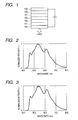
- FIG. 1 illustrates a constitution of a section of a white organic EL device corresponding to Example 1.
- FIG. 2 illustrates an EL spectrum of the white organic EL device produced in Example 1.
- FIG. 3 illustrates the EL spectrum of a white organic EL device produced in Example 2.
- FIG. 4 illustrates an emission mechanism for delayed fluorescence.
- FIGS. 5A and 5B are views for comparison between the emission mechanism for the delayed fluorescence and that for phosphorescence.
- FIG. 6 is a schematic view of an energy level where attention is paid to a sub-emission layer portion of a white organic EL device.
- FIG. 7 illustrates an organic EL device including a white organic EL device and a color filter.
- a white organic EL device for emitting white light includes: a substrate; an anode; a hole transport layer; an emission layer having a red sub-emission layer, a green sub-emission layer, and a blue sub-emission layer; and a cathode, the anode, the hole transport layer, the emission layer and the cathode being placed on the substrate in which: the green sub-emission layer is placed to be in contact with the hole transport layer; the red sub-emission layer is placed to be in contact with the green sub-emission layer, the blue sub-emission layer is placed to be in contact with the red sub-emission layer, the green sub-emission layer has a delayed fluorescent material; the red sub-emission layer has a phosphorescent light emitting material; an HOMO of the delayed fluorescent material is deeper than an HOMO of a material of the hole transport layer; and the HOMO of the delayed fluorescent material is shallower than an HOMO of the phosphorescent light emitting material.
- the green sub-emission layer having the delayed fluorescent material showing high efficiency is placed so as to be adjacent to the hole transport layer, so there is no need to widen a barrier between the HOMO's of the hole transport layer and the green sub-emission layer.
- the red sub-emission layer can emit light with high efficiency because the layer has the phosphorescent light emitting material.
- the HOMO of a host material for the green sub-emission layer is deeper than the HOMO of the material of the hole transport layer, and the HOMO of the host material for the green sub-emission layer is shallower than the HOMO of a host material for the red sub-emission layer.
- the HOMO and lowest unoccupied molecular orbital (LUMO) of the delayed fluorescent material are positioned between the HOMO and LUMO of the host material for the green sub-emission layer in terms of an energy diagram.
- the HOMO and LUMO of the phosphorescent light emitting material are also positioned between the HOMO and LUMO of the host material for the red sub-emission layer.
- the blue sub-emission layer be placed on a light extraction side; and the green sub-emission layer be placed so as to be more distant from the side than the blue sub-emission layer is.
- the blue sub-emission layer is placed on a side closer to the cathode than any other sub-emission layer is. Defining the cathode as an electrode on the light extraction side, that is, an electrode through which light transmits obviates the need for placing the blue sub-emission layer so that the layer may be most distant from the electrode on the light extraction side. The reason why such placement should be avoided is as follows: blue light has high energy, so the light must be prevented from passing through the green and red sub-emission layers to be emitted from the organic EL device to the outside to the extent possible.
- a fluorescent light emitting material cannot theoretically achieve an internal quantum efficiency of 100%, a phosphorescent light emitting material can theoretically achieve an internal quantum efficiency of 100%. While the fluorescent light emitting material emits light from its excited singlet state S1, the phosphorescent light emitting material emits light from its excited triplet state T1.
- the material requiring a lower energy for its light emission out of the two forestalls an increase in driving voltage.
- the energy depends on the S1 of a material. That is, when which one of the two materials requires higher energy for its light emission is determined, the S1's of the respective materials are compared, and the material having the higher S1 is regarded as requiring higher energy.
- the phosphorescent light emitting material requires higher energy for its light emission than the fluorescent light emitting material does. This is because of the following reason.
- the S1 of the fluorescent light emitting material and the T1 of the phosphorescent light emitting material are identical in energy when the materials emit lights of the same color. Since the S1 of a material is higher than the T1 of the material, the S1 of the phosphorescent light emitting material is higher than the S1 of the fluorescent light emitting material.
- the phosphorescent light emitting material increases the driving voltage.
- the fluorescent light emitting material has a low driving voltage and has low internal quantum efficiency.
- the phosphorescent light emitting material has a high driving voltage and has high internal quantum efficiency.
- the height of the S1 of a material is related to the width of the band gap of the material. That is, the higher the S1, the wider the band gap.
- organic EL device refers to a device having at least an emission layer and another layer between an anode and a cathode.
- the emission layer is obtained by laminating a green sub-emission layer, a red sub-emission layer, and a blue sub-emission layer, attention should be paid also to a barrier between sub-emission layers from the viewpoint of the injection of a carrier.
- the HOMO of the material is deep (distant) from a vacuum level
- the LUMO of the material is close to (shallow from) the vacuum level as compared to a material generally used in a layer where the above material should be used.
- the HOMO's or LUMO's of the materials show values substantially close to each other.
- the HOMO's of materials that can be used in a hole transport layer show values substantially close to each other irrespective of the kinds of the materials.
- a sub-emission layer adjacent to the hole transport layer is the green sub-emission layer having the delayed fluorescent material.
- the delayed fluorescent material has higher internal quantum efficiency than that of a fluorescent material; and the delayed fluorescent material has a lower S1 than that of a phosphorescent light emitting material that emits green light.
- a phosphorescent light emitting material having high internal quantum efficiency is used in the red sub-emission layer.
- the blue sub-emission layer is positioned so as to be closest to the light extraction side out of the sub-emission layers.
- FIG. 4 illustrates an emission mechanism for the delayed fluorescent material in the emission layer of the organic EL device.
- Excitons formed by recombination between holes and electrons in the emission layer are distributed as follows in accordance with their spin multiplicities: 25% of the excitons are distributed to an excited singlet state (S 1 ), and 75% of the excitons are distributed to an excited triplet state (T 1 ).
- S 1 excited singlet state
- T 1 excited triplet state
- the T 1 is thermally excited to the S 1 , and light emission occurs by virtue of an electron transition from the S 1 to an S 0 .
- all excitons in the S 1 and T 1 formed in the emission layer can each be extracted as light. Therefore, as in the case of phosphorescence, an upper limit for the internal quantum efficiency of the delayed fluorescent material can be set to 100% in principle.
- the delayed fluorescence of the present invention utilizes the thermal excitation from the T 1 to the S 1 . Therefore, the delayed fluorescence in the present invention is thermal excitation-type delayed fluorescence.
- FIGS. 5A and 5B schematically illustrate energy levels when the delayed fluorescence and phosphorescence have the same emission wavelength, and the energy levels are compared.
- the energy differences of the delayed fluorescence are smaller than those of phosphorescence.
- the following fact can be understood: as long as the delayed fluorescence and phosphorescence have the same emission wavelength, a band gap in the delayed fluorescence is smaller than that in phosphorescence.
- a light emitting material having a small band gap is used in an organic EL device.
- the organic EL device one or more organic layers are provided between an anode and a cathode.
- a barrier for injection from an electrode to an organic layer is of concern, and the driving voltage strongly depends on the barrier for injection.
- a barrier for injection between organic layers is similarly of concern. The use of the light emitting material having a small band gap can reduce the sizes of the above barriers for injection.
- the ease with which a hole is injected from the anode to an organic layer is improved, and the ease with which an electron is injected from the cathode to an organic layer is also improved. Therefore, the driving voltage can be reduced, and the power efficiency (lm/W) of the device can be improved in accordance with the increase.
- Examples of the delayed fluorescent material include a copper complex, a platinum complex, and a palladium complex. Examples of the delayed fluorescent material are shown below.
- the emission process of the delayed fluorescent material to be used in the present invention can be identified as the delayed fluorescence on the basis of the emission characteristics of the material.
- the emission of light from a compound capable of delayed fluorescence to be used in the present invention has the following characteristics:
- emission wavelength at room temperature In the case of ordinary fluorescence and phosphorescence, comparison between an emission wavelength at room temperature and an emission wavelength at the low temperature shows that the wavelengths are identical to each other, or the emission wavelength at the low temperature is shorter than the other. In contrast, in the case of the delayed fluorescence, an emission wavelength at the low temperature is longer than an emission wavelength at room temperature. This is because of the following reason: although light emission from a singlet is observed at room temperature, light emission occurs at low temperatures from the triplet which is a state lower in energy level than the singlet.
- emission wavelength refers to the maximum emission wavelength or the wavelength at which light emission starts.
- an emission lifetime is of the order of 10 -9 sec because light emission occurs from the singlet.
- an emission lifetime is of the order of 10 -6 sec.
- an emission lifetime is of the order of 10 -6 sec because the triplet is involved in light emission.
- the light emitting material used in the present invention preferably has an emission lifetime of 0.1 microsecond or more to less than 1 millisecond in a solid state or solution state.
- the emission lifetime of each of the delayed fluorescence and phosphorescence is at a level of 10 -6 sec; in the case of the delayed fluorescence, however, an emission lifetime at the low temperature is much longer than an emission lifetime at room temperature.
- an emission lifetime at the low temperature is at most ten times as long as an emission lifetime at room temperature.
- an emission lifetime strongly depends on temperatures because light emission occurs from different excited states at the low temperature and room temperature.
- the emission lifetime of the delayed fluorescence at the low temperature is ten or more times as long as the emission lifetime of the material at room temperature; depending on the kind of the compound, it may be observed that the former is two or more orders of magnitude longer than the latter.
- the emission lifetime of the light-emitting material used in the present invention shows the following characteristic when the material is in a solid state or solution state: an emission lifetime at the low temperature is 10 or more times, more specifically 50 or more times, or still more specifically 100 or more times as long as an emission lifetime at room temperature.
- the constitution of the white organic EL device is as follows: sub-emission layers for three colors, i.e., blue (B), green (G), and red (R) colors are laminated, and lights are simultaneously emitted from the layers and caused to undergo color mixture so that a white color may be obtained.
- B blue
- G green
- R red
- Examples of the combination of three color pixels, i.e., R, G, and B pixels each containing at least one delayed fluorescent material include, when DF, P, and F represent emission mechanisms for delayed fluorescence, phosphorescence, and fluorescence, respectively, (DF, P, P), (DF, DF, P), (DF, P, DF), (DF, DF, DF), (DF, F, F), (DF, DF, F), (DF, F, DF), (DF, P, F), (DF, F, P), (P, DF, P), (P, DF, DF), (F, DF, F), (F, DF, F), (F, DF, DF), (P, DF, F), (F, DF, P), (P, P, DF), (P, F, DF), (F, P, DF), (P, F, DF), (F, P, DF), and (F, F, DF).
- Reference numeral 103 represents an anode; 104, a hole transport layer; 105, a green sub-emission layer; 106, a red sub-emission layer; 107, a blue sub-emission layer; 108, an electron transport layer; and 109, a cathode.
- FIG. 6 is a schematic view illustrating the energy level of the white organic EL device.
- Each of the R, G, and B layers may be formed of a mixture of a host material and a light emitting dopant, or may be formed only of the light emitting dopant.
- the host material is a material having a large weight ratio in each sub-emission layer
- the light emitting dopant is a guest material having a small weight ratio in the layer.
- a band gap between the HOMO at the lower end and the LUMO at the upper end corresponds to the host material or the light emitting dopant.
- the HOMO and LUMO of each sub-emission layer correspond to the HOMO and LUMO of the host material.
- the HOMO and LUMO of the light emitting dopant for each of the R, G, and B sub-emission layers are not illustrated, in each sub-emission layer, the HOMO of the dopant is shallower than the HOMO of the host material, and the LUMO of the dopant is deeper than the LUMO of the host material.
- a delayed fluorescent material can reduce the band gap.
- a hole injection barrier between the hole transport layer and the green sub-emission layer is represented by ⁇ E 1
- an electron injection barrier between the electron transport layer and the blue sub-emission layer is represented by ⁇ E 2 -
- the ⁇ E 1 and ⁇ E 2 can be reduced in size because the band gaps of the green and blue sub-emission layers can be reduced.
- the driving voltage of the white organic EL device can be reduced, and the power efficiency of the device can be improved. It should be noted that, when the delayed fluorescence and phosphorescence in one host material are considered, a hole or electron can be easily injected for the delayed fluorescence having a small band gap as compared to phosphorescence, so the driving voltage of the white organic EL device is can be similarly reduced.
- the possibility that an electron is blocked increases in the green sub-emission layer. Accordingly, the possibility that a hole and an electron recombine in the entire emission layer increases. As a result, the efficiency of the white organic EL device can be improved.
- an organic EL device that emits light of any one of the three colors, i.e., the R, G, and B colors can be provided by mounting the white organic EL device with a color filter.
- the color filter itself absorbs light emitted from the white organic EL device, so total emission efficiency after passage through the color filter reduces. Therefore, a white organic EL device having additionally high efficiency and an additionally high luminance is absolutely necessary when the color filter is used.
- One approach to this end is to provide a white organic EL device which: has a low driving voltage; and consumes low power.
- FIG. 7 schematically illustrates an organic EL device having a color filter.
- a white light emitting device 111 is formed of R, G, and B sub-emission layers.
- Reference numeral 102 represents the color filter; 103, an anode; 109, a cathode; and 101, a transparent glass substrate.
- the delayed fluorescent material is used as a light emitting material for the white organic EL device.
- a white organic EL device is formed by laminating, on a substrate, an anode, a hole transport layer, an emission layer formed of multiple sub-emission layers, an electron transport layer, and a cathode.
- transparent glass is generally used here as the substrate, the substrate is not particularly limited as long as the substrate is transparent to such an extent that light can be extracted to the outside of the device.
- a hole injection layer or electron injection layer may be further provided for reducing the voltage at which the device is driven, and a carrier blocking layer or exciton blocking layer may be provided so as to be adjacent to the emission layer for improving the efficiency of the device.
- the following device constitution is described: the anode, the hole transport layer, the emission layer, the electron transport layer, and the cathode are laminated on a transparent glass substrate.
- ITO Indium tin oxide
- ITO has been consistently used in the anode in this embodiment as well; alternatively, an indium oxide/zinc oxide-based amorphous material (indium zinc oxide: IZO) or the like may be used.
- the thickness of the anode is not particularly limited.
- a method of forming the anode is, for example, a sputtering method, a vacuum evaporation method, or an ion plating method.
- any one of the known film formation methods such as a vacuum evaporation method, an ink jet method, and a spin coating method may be adopted as a method of forming the organic layers (the hole transport layer, the emission layer, and the electron transport layer) on ITO.
- the hole transport layer is not particularly limited as long as the layer has one of a function of injecting a hole from the anode and a function of transporting a hole.
- a material for the layer is specifically, for example, a conductive polymer such as an arylamine derivative, a carbazole derivative, or poly(3,4-ethylenedioxythiophene) (PEDOT-PSS).
- the order in which the sub-emission layers of the emission layer are laminated is not particularly limited.
- the respective sub-emission layers are not necessarily needed to be in contact with each other, and, for example, the following constitution may be adopted: a layer free of any light emitting dopant is interposed between two adjacent sub-emission layers.
- one sub-emission layer may contain multiple kinds of light emitting materials different from each other in emission wavelength.
- the term "multiple kinds" as used herein refers to any one of a delayed fluorescent material, a phosphorescent material, and a fluorescent material.
- a host material for the emission layer is not particularly limited as long as the host material efficiently supplies the energy of an exciton to a guest material for each color.
- the electron transport layer is not particularly limited as long as the layer has one of a function of injecting an electron from the cathode and a function of transporting an electron.
- a metal complex such as bathophenanthroline (Bphen), 4-biphenyloxolatoaluminum (III) bis(2-methyl-8-quinolinato)-4-phenylphenolate (BAlq 3 ), or a quinolinol derivative can be used.
- the cathode is formed on the electron transport layer.
- a metal, alloy, or the like having a small work function is used in the cathode.
- magnesium, lithium, a magnesium/aluminum alloy, or the like may be used.
- a lighting unit can be provided by using the organic EL device according to the present invention.
- the emission of white light in the present invention is as follows: the light has chromaticity coordinates (X, Y) in a CIE1931 colorimetric system of preferably (0.33 ⁇ 0.15, 0.33 ⁇ 0.15), or more preferably (0.33 ⁇ 0.07, 0.33 ⁇ 0.07).
- the direction in which light is extracted may be of a bottom emission type in which light is extracted from the side same as a substrate, or may be of a top emission type in which light is extracted from the side opposite to a substrate.
- the cathode is desirably a transparent electrode using a transparent material
- the anode is desirably of such a constitution that a reflective electrode using a reflective metal and a transparent electrode are laminated. With such constitution, light extraction efficiency can be improved by utilizing optical interference.
- the white organic EL device according to the present invention may be used as a pixel in a display apparatus.
- the following constitution may be adopted: each of multiple pixels is connected to a switching device such as a TFT so that the luminance of the device may be controlled by the switching device.
- a specific constitution of a white organic EL device is shown.
- ITO/ ⁇ -NPD 40 nm/CBP+10 mass% [Cu(tsmp)] 2 (60 nm)/CBP+10 mass% Ir(piq) 3 (80 nm)/CDBP+10 mass% FIrpic (30 nm)/BCP (40 nm)/LiF (0.5 nm)/Al (100 nm)
- an ITO film 120 nm was formed on a transparent glass substrate serving as a support member and having a thickness of 1.1 mm by a sputtering method, and the resultant was used as an anode side transparent electrode.
- the electrode was subjected to ultrasonic cleaning with 2-propanol (IPA) and boil washing, and was then dried. After that, the electrode was subjected to UV/O 3 cleaning, and ⁇ -NPD (Compound 3) was deposited from the vapor in a vacuum onto the electrode to serve as a hole transport layer.
- IPA 2-propanol
- ⁇ -NPD Compound 3
- Film formation was performed under the following conditions: the pressure in the chamber of a vacuum evaporator was reduced so that a degree of vacuum in the chamber might be 5 ⁇ 10 -5 Pa, and then an evaporation rate was stabilized.
- the thickness of the hole transport layer formed of ⁇ -NPD was set to 40 nm.
- Hole transport layer ⁇ -NPD (Compound 3)
- Sub-emission layers for three colors i.e., green, red, and blue sub-emission layers were formed by laminating on the hole transport layer in the stated order by a vacuum evaporation method.
- a delayed fluorescent material [Cu(tsmp)] 2 (Compound 1) was used as a dopant for the green sub-emission layer
- a phosphorescent material Ir(piq) 3 (Compound 4) was used as a dopant for the red sub-emission layer
- a phosphorescent material FIrpic Compound 5
- CBP Compound 6
- CDBP Compound 7
- Red dopant phosphorescent material Ir(piq) 3 (Compound 4) 10 mass%
- Evaporation rates for each sub-emission layer were as follows: the host material and the dopant material were co-evaporated at rates of 0.9 ⁇ /sec and 0.1 ⁇ /sec, respectively (at a doping ratio of 10 mass%).
- the green sub-emission layer had a thickness of 60 nm
- the red sub-emission layer had a thickness of 80 nm
- the blue sub-emission layer had a thickness of 30 nm.
- BCP (Compound 8) was formed into a film on the blue sub-emission layer to serve as an electron transport layer by vacuum evaporation.
- the layer had a thickness of 40 nm.
- Electron transport layer BCP (Compound 8)
- Aluminum (Al) having a 0.5 nm layer of lithium fluoride (LiF) provided on its surface was formed on the electron transport layer to serve as a cathode by a vacuum evaporation method.
- the cathode had a thickness of 100 nm.
- FIG. 2 illustrates the EL spectrum of the white organic EL device produced in Example 1.
- the device emitted good white light having chromaticity coordinates (X, Y) in a CIE1931 colorimetric system of (0.34, 0.32) at a front luminance of 1,000 cd/m 2 ; further, the device stably emitted light while maintaining a color purity even after having been energized for 2 hours.
- This example relates to a white organic EL device in which light is extracted from the side opposite to a transparent glass substrate.
- a TFT driver circuit formed of low-temperature polysilicon was formed on the transparent glass substrate serving as a support member, and a planarization film formed of an acrylic resin was formed on the circuit.
- a silver alloy (AgCuNd) was patterned into a film having a thickness of 100 nm on the film to serve as a reflective electrode by a sputtering method.
- IZO was patterned into a film having a thickness of 30 nm on the reflective electrode to serve as a transparent electrode by a sputtering method.
- an anode as a lower electrode was formed.
- a device isolation film was formed of an acrylic resin.
- an anode side transparent electrode substrate was produced.
- the substrate was subjected to ultrasonic cleaning with IPA and boil washing, and was then dried. After that, the substrate was subjected to UV/O 3 cleaning, and a hole transport layer, G, R, and B sub-emission layers, and an electron transport layer were sequentially laminated in the same manner as in Example 1.
- a co-evaporated film of BCP and Cs 2 CO 3 (at a weight ratio of 9:1) having a thickness of 14 nm was formed on the electron transport layer to serve as an electron injection layer at a degree of vacuum of 2.0 ⁇ 10 -4 Pa.
- silver (Ag) was formed into a film having a thickness of 15 nm to serve as a cathode by a vacuum evaporation method at a degree of vacuum of 2.0 ⁇ 10 -4 Pa.
- FIG. 3 illustrates the EL spectrum of the white organic EL device.
- the following facts were observed: the device emitted good white light having chromaticity coordinates (X, Y) in a CIE1931 colorimetric system of (0.34, 0.34) at a front luminance of 1,000 cd/m 2 ; further, the device stably emitted light while maintaining a color purity even after having been energized for 2 hours.
- a high-efficiency, white organic electroluminescent device has such a structure that its emission layer is obtained by laminating sub-emission layers of red, green, and blue, respectively.
- the green sub-emission layer contacting a hole transport layer has a delayed fluorescent material
- the red sub-emission layer has a phosphorescent light emitting material.
Landscapes
- Physics & Mathematics (AREA)
- Optics & Photonics (AREA)
- Electroluminescent Light Sources (AREA)
Applications Claiming Priority (2)
| Application Number | Priority Date | Filing Date | Title |
|---|---|---|---|
| JP2008264426 | 2008-10-10 | ||
| JP2009222632A JP2010114070A (ja) | 2008-10-10 | 2009-09-28 | 白色有機el素子 |
Publications (2)
| Publication Number | Publication Date |
|---|---|
| EP2175503A2 true EP2175503A2 (de) | 2010-04-14 |
| EP2175503A3 EP2175503A3 (de) | 2011-04-13 |
Family
ID=41514839
Family Applications (1)
| Application Number | Title | Priority Date | Filing Date |
|---|---|---|---|
| EP09172514A Withdrawn EP2175503A3 (de) | 2008-10-10 | 2009-10-08 | Weiße organische elektrolumineszente Anzeigevorrichtung |
Country Status (5)
| Country | Link |
|---|---|
| US (1) | US8076681B2 (de) |
| EP (1) | EP2175503A3 (de) |
| JP (1) | JP2010114070A (de) |
| KR (1) | KR20100040681A (de) |
| CN (1) | CN101728490B (de) |
Cited By (7)
| Publication number | Priority date | Publication date | Assignee | Title |
|---|---|---|---|---|
| US8076841B2 (en) * | 2008-10-10 | 2011-12-13 | Canon Kabushiki Kaisha | Organic electroluminescent display apparatus |
| US9252372B2 (en) | 2008-07-17 | 2016-02-02 | Merck Patent Gmbh | Complexes for use in optoelectronic components |
| WO2016041802A1 (en) * | 2014-09-16 | 2016-03-24 | Cynora Gmbh | Light-emitting layer suitable for bright luminescence |
| EP2980877A4 (de) * | 2013-03-29 | 2016-10-26 | Univ Kyushu Nat Univ Corp | Organisches elektrolumineszentes element |
| US20170309857A1 (en) | 2014-10-31 | 2017-10-26 | Kyushu University, National University Corporation | Organic light-emitting device |
| US10164206B2 (en) | 2012-04-20 | 2018-12-25 | Semiconductor Energy Laboratory Co., Ltd. | Light-emitting element, light-emitting device, display device, electronic device, and lighting device |
| US11133482B2 (en) | 2014-09-30 | 2021-09-28 | Semiconductor Energy Laboratory Co., Ltd. | Light-emitting element, display device, electronic device, and lighting device |
Families Citing this family (22)
| Publication number | Priority date | Publication date | Assignee | Title |
|---|---|---|---|---|
| CN105762279B (zh) | 2011-03-25 | 2018-04-17 | 出光兴产株式会社 | 有机电致发光器件 |
| WO2013005028A1 (en) | 2011-07-04 | 2013-01-10 | Cambridge Display Technology Limited | Organic light emitting device and fabrication method thereof |
| KR20140106631A (ko) * | 2011-12-02 | 2014-09-03 | 고쿠리쓰다이가쿠호진 규슈다이가쿠 | 유기 발광 소자 그리고 그것에 사용하는 지연 형광 재료 및 화합물 |
| JP6367386B2 (ja) * | 2012-04-20 | 2018-08-01 | 株式会社半導体エネルギー研究所 | 発光素子、照明装置、発光装置、表示装置、電子機器 |
| DE102013214661B4 (de) * | 2012-08-03 | 2023-01-05 | Semiconductor Energy Laboratory Co., Ltd. | Licht emittierendes Element, Licht emittierende Vorrichtung und Beleuchtungsvorrichtung |
| US10957870B2 (en) | 2012-09-07 | 2021-03-23 | Universal Display Corporation | Organic light emitting device |
| JP5818870B2 (ja) * | 2012-12-27 | 2015-11-18 | キヤノン株式会社 | 有機発光素子及び表示装置 |
| WO2014157610A1 (ja) * | 2013-03-29 | 2014-10-02 | コニカミノルタ株式会社 | 有機エレクトロルミネッセンス素子、照明装置、表示装置、有機ルミネッセンス素子用発光性薄膜と組成物及び発光方法 |
| WO2014163083A1 (ja) * | 2013-04-05 | 2014-10-09 | コニカミノルタ株式会社 | 発光層形成用塗布液、有機エレクトロルミネッセンス素子とその製造方法及び照明・表示装置 |
| US10249828B2 (en) | 2013-04-08 | 2019-04-02 | Merck Patent Gmbh | Organic electroluminescent device |
| CN105103328B (zh) | 2013-04-08 | 2018-06-05 | 默克专利有限公司 | 具有延迟荧光的有机发光器件 |
| KR102361072B1 (ko) | 2013-04-08 | 2022-02-09 | 메르크 파텐트 게엠베하 | 열 활성화 지연 형광 재료를 갖는 유기 전계발광 디바이스 |
| JP6305068B2 (ja) | 2013-04-30 | 2018-04-04 | キヤノン株式会社 | 有機発光素子 |
| JP6417689B2 (ja) * | 2014-03-25 | 2018-11-07 | 凸版印刷株式会社 | 有機el発光装置 |
| EP2950362B1 (de) | 2014-05-26 | 2021-03-24 | LG Display Co., Ltd. | Vorrichtung zur emission von weissem organischem licht |
| JP2016092280A (ja) * | 2014-11-07 | 2016-05-23 | コニカミノルタ株式会社 | 発光性薄膜、有機エレクトロルミネッセンス素子、照明装置及び表示装置 |
| CN105322099B (zh) * | 2015-11-30 | 2018-01-05 | 华南理工大学 | 一种全荧光白光有机发光二极管及其制备方法 |
| US10854838B2 (en) * | 2015-12-08 | 2020-12-01 | Idemitsu Kosan Co., Ltd. | Organic EL light emitting apparatus and electronic instrument |
| JP6739804B2 (ja) * | 2015-12-28 | 2020-08-12 | 国立大学法人九州大学 | 有機エレクトロルミネッセンス素子 |
| US10403841B2 (en) * | 2016-02-10 | 2019-09-03 | Sharp Kabushiki Kaisha | Organic electroluminescent element and organic electroluminescent display device |
| CN106328818B (zh) * | 2016-08-26 | 2018-11-20 | 深圳市华星光电技术有限公司 | 荧光/磷光混合型白光有机发光二极管 |
| CN115020601B (zh) * | 2022-06-02 | 2025-08-01 | 湖北长江新型显示产业创新中心有限公司 | 一种白光电致发光元件、显示面板、光源和显示装置 |
Citations (2)
| Publication number | Priority date | Publication date | Assignee | Title |
|---|---|---|---|---|
| JPH06207170A (ja) | 1992-11-20 | 1994-07-26 | Idemitsu Kosan Co Ltd | 白色有機エレクトロルミネッセンス素子 |
| JP2004241374A (ja) | 2003-01-17 | 2004-08-26 | Sogo Pharmaceutical Co Ltd | 有機エレクトロルミネッセンス素子 |
Family Cites Families (27)
| Publication number | Priority date | Publication date | Assignee | Title |
|---|---|---|---|---|
| AU2002305548A1 (en) * | 2001-05-16 | 2002-11-25 | The Trustees Of Princeton University | High efficiency multi-color electro-phosphorescent oleds |
| CN101159319A (zh) | 2002-10-24 | 2008-04-09 | 株式会社丰田自动织机 | 有机电致发光器件 |
| JP2004200141A (ja) * | 2002-10-24 | 2004-07-15 | Toyota Industries Corp | 有機el素子 |
| JP3840235B2 (ja) * | 2003-06-27 | 2006-11-01 | キヤノン株式会社 | 有機発光素子 |
| TWI278504B (en) * | 2003-11-04 | 2007-04-11 | Lg Chemical Ltd | New compound capable of being used in organic layer of organic light emitting device |
| JP4086817B2 (ja) * | 2004-07-20 | 2008-05-14 | キヤノン株式会社 | 有機el素子 |
| DE502005002342D1 (de) * | 2005-03-15 | 2008-02-07 | Novaled Ag | Lichtemittierendes Bauelement |
| US9070884B2 (en) * | 2005-04-13 | 2015-06-30 | Universal Display Corporation | Hybrid OLED having phosphorescent and fluorescent emitters |
| US7768194B2 (en) * | 2005-06-01 | 2010-08-03 | The Trustees Of Princeton University | Fluorescent filtered electrophosphorescence |
| KR100672535B1 (ko) * | 2005-07-25 | 2007-01-24 | 엘지전자 주식회사 | 유기 el 소자 및 그 제조방법 |
| US20070126350A1 (en) * | 2005-12-06 | 2007-06-07 | Lee Jeong I | White organic light emitting device |
| KR20070073454A (ko) * | 2006-01-05 | 2007-07-10 | 삼성에스디아이 주식회사 | 유기 전계 발광 소자 |
| KR101313094B1 (ko) * | 2006-01-24 | 2013-12-31 | 삼성디스플레이 주식회사 | 1,8-나프탈이미드기를 가진 고분자 및 상기 고분자를포함하는 유기 발광 소자 |
| TWI296901B (en) * | 2006-02-23 | 2008-05-11 | Au Optronics Corp | Organic electro-luminescence device |
| WO2007145976A2 (en) * | 2006-06-05 | 2007-12-21 | E. I. Du Pont De Nemours And Company | Process for making an organic light-emitting diode |
| JP5061184B2 (ja) * | 2006-06-05 | 2012-10-31 | イー・アイ・デュポン・ドウ・ヌムール・アンド・カンパニー | 有機発光ダイオードの形成方法、およびその方法によって製造されたデバイス |
| JP4865411B2 (ja) * | 2006-06-15 | 2012-02-01 | キヤノン株式会社 | 有機発光素子、ディスプレイ装置および表示装置 |
| GB2442724B (en) * | 2006-10-10 | 2009-10-21 | Cdt Oxford Ltd | Light emissive device |
| US8945722B2 (en) * | 2006-10-27 | 2015-02-03 | The University Of Southern California | Materials and architectures for efficient harvesting of singlet and triplet excitons for white light emitting OLEDs |
| KR100846590B1 (ko) * | 2006-11-08 | 2008-07-16 | 삼성에스디아이 주식회사 | 실란일아민계 화합물, 이의 제조 방법 및 이를 포함한유기막을 구비한 유기 발광 소자 |
| JP5153127B2 (ja) * | 2006-11-28 | 2013-02-27 | キヤノン株式会社 | アミン化合物及び有機発光素子 |
| US8207526B2 (en) * | 2007-03-23 | 2012-06-26 | Idemitsu Kosan Co., Ltd. | Organic EL device |
| US20080286610A1 (en) * | 2007-05-17 | 2008-11-20 | Deaton Joseph C | Hybrid oled with fluorescent and phosphorescent layers |
| KR101407578B1 (ko) * | 2007-07-24 | 2014-06-13 | 삼성디스플레이 주식회사 | 페닐페녹사진 또는 페닐페노시아진계 화합물 및 이를이용한 유기 전계 발광 소자 |
| DE102007058005B4 (de) * | 2007-09-25 | 2018-05-17 | Osram Oled Gmbh | Strahlungsemittierende Vorrichtung und Verfahren zu deren Herstellung |
| US20090091255A1 (en) * | 2007-10-09 | 2009-04-09 | Sung-Hoon Lee | White organic light emitting device |
| KR100922760B1 (ko) * | 2008-03-03 | 2009-10-21 | 삼성모바일디스플레이주식회사 | 유기 발광 소자 |
-
2009
- 2009-09-28 JP JP2009222632A patent/JP2010114070A/ja not_active Withdrawn
- 2009-10-05 US US12/573,367 patent/US8076681B2/en active Active
- 2009-10-08 KR KR1020090095484A patent/KR20100040681A/ko not_active Ceased
- 2009-10-08 EP EP09172514A patent/EP2175503A3/de not_active Withdrawn
- 2009-10-10 CN CN2009101784778A patent/CN101728490B/zh active Active
Patent Citations (2)
| Publication number | Priority date | Publication date | Assignee | Title |
|---|---|---|---|---|
| JPH06207170A (ja) | 1992-11-20 | 1994-07-26 | Idemitsu Kosan Co Ltd | 白色有機エレクトロルミネッセンス素子 |
| JP2004241374A (ja) | 2003-01-17 | 2004-08-26 | Sogo Pharmaceutical Co Ltd | 有機エレクトロルミネッセンス素子 |
Non-Patent Citations (2)
| Title |
|---|
| "IUPAC Compendium of Chemical Terminology, 2nd Edition; Delayed Fluorescence", 1 January 1997, COMPENDIUM OF CHEMICAL TERMINOLOGY. INTERNATIONAL UNION OF PURE & APPLIED CHEMISTRY (IUPAC), article "IUPAC Compendium of Chemical Terminology, 2nd Edition; Delayed Fluorescence", XP055022700 * |
| GIEBINK N C ET AL: "Transient analysis of triplet exciton dynamics in amorphous organic semiconductor thin films", ORGANIC ELECTRONICS, ELSEVIER, AMSTERDAM, NL, vol. 7, no. 5, 1 October 2006 (2006-10-01), pages 375 - 386, XP024972796, ISSN: 1566-1199, [retrieved on 20061001], DOI: 10.1016/J.ORGEL.2006.04.007 * |
Cited By (18)
| Publication number | Priority date | Publication date | Assignee | Title |
|---|---|---|---|---|
| US9252372B2 (en) | 2008-07-17 | 2016-02-02 | Merck Patent Gmbh | Complexes for use in optoelectronic components |
| US8076841B2 (en) * | 2008-10-10 | 2011-12-13 | Canon Kabushiki Kaisha | Organic electroluminescent display apparatus |
| US11177451B2 (en) | 2012-04-20 | 2021-11-16 | Semiconductor Energy Laboratory Co., Ltd. | Light-emitting element, light-emitting device, display device, electronic device, and lighting device |
| US10505135B2 (en) | 2012-04-20 | 2019-12-10 | Semiconductor Energy Laboratory Co., Ltd. | Light-emitting element, light-emitting device, display device, electronic device, and lighting device |
| US12127419B2 (en) | 2012-04-20 | 2024-10-22 | Semiconductor Energy Laboratory Co., Ltd. | Light-emitting element, light-emitting device, display device, electronic device, and lighting device |
| US11778846B2 (en) | 2012-04-20 | 2023-10-03 | Semiconductor Energy Laboratory Co., Ltd. | Light-emitting element, light-emitting device, display device, electronic device, and lighting device |
| US10164206B2 (en) | 2012-04-20 | 2018-12-25 | Semiconductor Energy Laboratory Co., Ltd. | Light-emitting element, light-emitting device, display device, electronic device, and lighting device |
| US10797257B2 (en) | 2012-04-20 | 2020-10-06 | Semiconductor Energy Laboratory Co., Ltd. | Light-emitting element, light-emitting device, display device, electronic device, and lighting device |
| US10600983B2 (en) | 2013-03-29 | 2020-03-24 | Kyulux, Inc. | Organic electroluminescent device comprising delayed fluorescent materials |
| EP2980877A4 (de) * | 2013-03-29 | 2016-10-26 | Univ Kyushu Nat Univ Corp | Organisches elektrolumineszentes element |
| WO2016041802A1 (en) * | 2014-09-16 | 2016-03-24 | Cynora Gmbh | Light-emitting layer suitable for bright luminescence |
| US11367848B2 (en) | 2014-09-16 | 2022-06-21 | Cynora Gmbh | Light-emitting layer suitable for bright luminescence |
| US11133482B2 (en) | 2014-09-30 | 2021-09-28 | Semiconductor Energy Laboratory Co., Ltd. | Light-emitting element, display device, electronic device, and lighting device |
| US11557742B2 (en) | 2014-09-30 | 2023-01-17 | Semiconductor Energy Laboratory Co., Ltd. | Light-emitting element and display device including compound having function of emitting TADF at room temperature |
| US12495662B2 (en) | 2014-09-30 | 2025-12-09 | Semiconductor Energy Laboratory Co., Ltd. | Light-emitting element and display device including TADF compound |
| US10290824B2 (en) | 2014-10-31 | 2019-05-14 | Kyushu University, National University Corporation | Organic light-emitting device |
| EP3214666A4 (de) * | 2014-10-31 | 2018-06-13 | Kyushu University National University Corporation | Organisches leuchtelement |
| US20170309857A1 (en) | 2014-10-31 | 2017-10-26 | Kyushu University, National University Corporation | Organic light-emitting device |
Also Published As
| Publication number | Publication date |
|---|---|
| CN101728490B (zh) | 2012-01-11 |
| JP2010114070A (ja) | 2010-05-20 |
| EP2175503A3 (de) | 2011-04-13 |
| KR20100040681A (ko) | 2010-04-20 |
| CN101728490A (zh) | 2010-06-09 |
| US8076681B2 (en) | 2011-12-13 |
| US20100090238A1 (en) | 2010-04-15 |
Similar Documents
| Publication | Publication Date | Title |
|---|---|---|
| US8076681B2 (en) | White organic electroluminescent device | |
| CN100407448C (zh) | 基于电致磷光的极高效有机发光器件 | |
| JP3589960B2 (ja) | 有機el素子 | |
| US6303238B1 (en) | OLEDs doped with phosphorescent compounds | |
| CN100484349C (zh) | 有机发光元件 | |
| US7928650B2 (en) | Organic EL display apparatus | |
| US20140326976A1 (en) | Organic electroluminescent element | |
| JP2010114428A (ja) | 有機el表示装置 | |
| US10879496B2 (en) | Organic electroluminescent element having a charge generating layer between adjacent light emitting layers | |
| JP2014011208A (ja) | 有機エレクトロルミネッセント素子及び照明装置 | |
| KR102491790B1 (ko) | 유기전계발광소자 | |
| JP5735162B1 (ja) | 有機エレクトロルミネッセント素子及び照明装置 | |
| US12287075B2 (en) | Organic light emitting display device and lighting apparatus for vehicles using the same | |
| KR20100073417A (ko) | 유기전계발광소자 | |
| JP5857006B2 (ja) | 有機エレクトロルミネッセント素子及び照明装置 | |
| KR101101940B1 (ko) | 이중 도핑을 이용한 고효율 진적색 인광 유기발광소자 및 그 제조 방법 | |
| JP2007235081A (ja) | 有機led素子 | |
| JP2010177462A (ja) | 有機el素子 |
Legal Events
| Date | Code | Title | Description |
|---|---|---|---|
| PUAI | Public reference made under article 153(3) epc to a published international application that has entered the european phase |
Free format text: ORIGINAL CODE: 0009012 |
|
| AK | Designated contracting states |
Kind code of ref document: A2 Designated state(s): AT BE BG CH CY CZ DE DK EE ES FI FR GB GR HR HU IE IS IT LI LT LU LV MC MK MT NL NO PL PT RO SE SI SK SM TR |
|
| PUAL | Search report despatched |
Free format text: ORIGINAL CODE: 0009013 |
|
| AK | Designated contracting states |
Kind code of ref document: A3 Designated state(s): AT BE BG CH CY CZ DE DK EE ES FI FR GB GR HR HU IE IS IT LI LT LU LV MC MK MT NL NO PL PT RO SE SI SK SM TR |
|
| 17P | Request for examination filed |
Effective date: 20111013 |
|
| 17Q | First examination report despatched |
Effective date: 20120328 |
|
| STAA | Information on the status of an ep patent application or granted ep patent |
Free format text: STATUS: THE APPLICATION HAS BEEN WITHDRAWN |
|
| 18W | Application withdrawn |
Effective date: 20120719 |