EP2175523A1 - Reflektor und Antenne die einen solchen Reflektor umfasst - Google Patents
Reflektor und Antenne die einen solchen Reflektor umfasst Download PDFInfo
- Publication number
- EP2175523A1 EP2175523A1 EP09171108A EP09171108A EP2175523A1 EP 2175523 A1 EP2175523 A1 EP 2175523A1 EP 09171108 A EP09171108 A EP 09171108A EP 09171108 A EP09171108 A EP 09171108A EP 2175523 A1 EP2175523 A1 EP 2175523A1
- Authority
- EP
- European Patent Office
- Prior art keywords
- radiating
- radiating element
- metal patch
- pattern
- radiating elements
- Prior art date
- Legal status (The legal status is an assumption and is not a legal conclusion. Google has not performed a legal analysis and makes no representation as to the accuracy of the status listed.)
- Granted
Links
Images


Classifications
-
- H—ELECTRICITY
- H01—ELECTRIC ELEMENTS
- H01Q—ANTENNAS, i.e. RADIO AERIALS
- H01Q21/00—Antenna arrays or systems
-
- H—ELECTRICITY
- H01—ELECTRIC ELEMENTS
- H01Q—ANTENNAS, i.e. RADIO AERIALS
- H01Q19/00—Combinations of primary active antenna elements and units with secondary devices, e.g. with quasi-optical devices, for giving the antenna a desired directional characteristic
- H01Q19/10—Combinations of primary active antenna elements and units with secondary devices, e.g. with quasi-optical devices, for giving the antenna a desired directional characteristic using reflecting surfaces
- H01Q19/104—Combinations of primary active antenna elements and units with secondary devices, e.g. with quasi-optical devices, for giving the antenna a desired directional characteristic using reflecting surfaces using a substantially flat reflector for deflecting the radiated beam, e.g. periscopic antennas
-
- H—ELECTRICITY
- H01—ELECTRIC ELEMENTS
- H01Q—ANTENNAS, i.e. RADIO AERIALS
- H01Q13/00—Waveguide horns or mouths; Slot antennas; Leaky-waveguide antennas; Equivalent structures causing radiation along the transmission path of a guided wave
- H01Q13/10—Resonant slot antennas
-
- H—ELECTRICITY
- H01—ELECTRIC ELEMENTS
- H01Q—ANTENNAS, i.e. RADIO AERIALS
- H01Q15/00—Devices for reflection, refraction, diffraction or polarisation of waves radiated from an antenna, e.g. quasi-optical devices
- H01Q15/0006—Devices acting selectively as reflecting surface, as diffracting or as refracting device, e.g. frequency filtering or angular spatial filtering devices
- H01Q15/0013—Devices acting selectively as reflecting surface, as diffracting or as refracting device, e.g. frequency filtering or angular spatial filtering devices said selective devices working as frequency-selective reflecting surfaces, e.g. FSS, dichroic plates, surfaces being partly transmissive and reflective
- H01Q15/002—Devices acting selectively as reflecting surface, as diffracting or as refracting device, e.g. frequency filtering or angular spatial filtering devices said selective devices working as frequency-selective reflecting surfaces, e.g. FSS, dichroic plates, surfaces being partly transmissive and reflective said selective devices being reconfigurable or tunable, e.g. using switches or diodes
-
- H—ELECTRICITY
- H01—ELECTRIC ELEMENTS
- H01Q—ANTENNAS, i.e. RADIO AERIALS
- H01Q19/00—Combinations of primary active antenna elements and units with secondary devices, e.g. with quasi-optical devices, for giving the antenna a desired directional characteristic
- H01Q19/10—Combinations of primary active antenna elements and units with secondary devices, e.g. with quasi-optical devices, for giving the antenna a desired directional characteristic using reflecting surfaces
-
- H—ELECTRICITY
- H01—ELECTRIC ELEMENTS
- H01Q—ANTENNAS, i.e. RADIO AERIALS
- H01Q21/00—Antenna arrays or systems
- H01Q21/06—Arrays of individually energised antenna units similarly polarised and spaced apart
- H01Q21/061—Two dimensional planar arrays
-
- H—ELECTRICITY
- H01—ELECTRIC ELEMENTS
- H01Q—ANTENNAS, i.e. RADIO AERIALS
- H01Q3/00—Arrangements for changing or varying the orientation or the shape of the directional pattern of the waves radiated from an antenna or antenna system
- H01Q3/44—Arrangements for changing or varying the orientation or the shape of the directional pattern of the waves radiated from an antenna or antenna system varying the electric or magnetic characteristics of reflecting, refracting, or diffracting devices associated with the radiating element
- H01Q3/46—Active lenses or reflecting arrays
Definitions
- the present invention relates to a reflector array for a reflector array antenna. It applies in particular to antennas mounted on a spacecraft such as a telecommunications satellite or antennas terrestrial terminals for telecommunications or satellite broadcasting systems.
- a reflecting array antenna 10 (in English: reflectarray antenna) as represented for example on the figure 1 , comprises a set of elementary radiating elements 12 assembled in a network 11 with one or two dimensions and forming a reflective surface 14 making it possible to increase the directivity and the gain of the antenna 10.
- the elementary radiating elements also called elementary cells, of the reflective network, of the metal patch and / or slot type, have variable parameters, such as, for example, the geometric dimensions of the etched patterns (length and width of the "patches" or slots) which are adjusted so as to obtain a diagram selected radiation.
- the elementary radiating elements 12 may consist of metal patches loaded with radiating slots and separated from a metal ground plane of a typical distance between ⁇ g / 10 and ⁇ g / 6, where ⁇ g is the guided wavelength. in the spacer medium.
- This spacer medium may be a dielectric, but also a composite sandwich made by a symmetrical arrangement of a honeycomb type separator and dielectric skins thin thicknesses.
- the elementary cell must be able to precisely control the phase shift it produces on an incident wave, for the different frequencies of the bandwidth. It is also necessary that the manufacturing process of the reflector network is as simple as possible.
- the arrangement (in English: lay-out) of the radiating elements in the reflector network requires significant attention. It must respect, at least approximately, a strong periodicity which defines the characteristics in reflection of the reflector network (typically less than 0.65 ⁇ and preferably equal to 0.5 ⁇ , where ⁇ is the wavelength in free space). As explained below, the higher the periodicity, the better the performance. However currently known reflector networks present a major problem.
- the arrangement of the elementary radiating elements with respect to each other to form a reflector array is synthesized so as to obtain a given radiation pattern in a pointing direction chosen to achieve a given coverage.
- the figure 3a shows an example of arrangement of the radiating elements of a reflector array antenna according to the prior art, to obtain a directional beam pointed in a lateral direction relative to the antenna. Due to the flatness of the reflector network and the differences in path lengths of a wave emitted by a primary source 13 to each radiating element of the grating, the illumination of the reflector network by an incident wave from a primary source 13 causes a phase distribution of the electromagnetic field above the reflecting surface 14.
- the dimensions of the radiating elements are thus defined so that the incident wave is reflected by the grating 11 with a phase shift which compensates the relative phase of the incident wave.
- the radiating elements 12 are therefore not all surrounded by similar elements, and the transitions from one radiating element to another are all the more important as the phase variation is rapid.
- the object of the present invention is to overcome these drawbacks by proposing a reflector grating which does not introduce strong breaks in the periodicity of the radiating elements on the reflecting surface and thus making it possible to reduce the disturbances in the radiation pattern and to improve the directivity the network antenna comprising such a reflector network.
- Another object of the invention is to provide a reflective grating which makes it possible to reduce the number of transitions while increasing the possibilities of variation of the phase of the waves reflected by the radiating elements.
- a final object of the invention is to provide a reflector network comprising elementary radiating elements having a simple and compact radiating structure.
- the aperture may be an annular gap having a progressively increasing electrical length from one radiating element to another adjacent radiating element
- the metal patch may be a metal ring having an evolutive width from one radiating element to another element. radiating adjacent.
- the pattern may comprise at least one radiating element comprising at least one metal patch and two concentric annular slots made in the metal patch.
- the pattern may comprise a plurality of radiating elements comprising a metal patch and several concentric annular slots made in the metal patch, at least one of the annular slots of a radiating element having an evolutionary electrical length relative to another adjacent radiating element.
- the pattern may comprise a radiating element comprising a complete metal patch and a plurality of consecutive radiating elements comprising a metal patch and a plurality of concentric annular slots in the metal patch, the annular slots having an evolutionary length independently or simultaneously of a radiating element with another radiating element adjacent.
- the pattern may comprise at least one radiating element comprising an annular slot or a plurality of concentric annular slots and at least one short-circuit means and / or capacitive means placed in at least one annular slot, the short-circuit means and / or the capacitive means varying the electrical length of the slot.
- the short-circuit means may be a metallization sectioning the slot at a predetermined location and length or a microswitch.
- each radiating element of the pattern may comprise at least one micro-switch, each micro-switch being positioned in an annular slot at a predetermined location and in a chosen open or closed state, all the annular slots having the same width.
- the pattern may comprise several consecutive radiating elements comprising a plurality of concentric annular slots, all the radiating elements comprising the same number of microswitches positioned at the same locations in the annular slots, the microswitches of all the radiating elements of the pattern being configured. in different states, the states of the micro-switches gradually varying from one radiating element to another adjacent radiating element.
- the radiating elements have a geometric shape chosen from a hexagon shape or a cross shape with two perpendicular branches.
- the invention also relates to a reflector array antenna comprising at least one reflector array.
- the figure 1 shows an example of a reflector array antenna having an optimized reflector array 11, as described hereinafter, forming a periodic reflective surface 14 and a primary source 13 for illuminating the reflector array 11 with an incident wave.
- FIG. 2 On the figure 2 is shown an example of elementary radiating element 12 of square shape having sides of length m, comprising a metal patch 15 printed on an upper face of a dielectric substrate 16 provided with a metal ground plane 17 on its underside.
- the metal patch 15 has a square shape having sides of dimension p and has two slots 18 of length b and width k practiced at its center, the slots being arranged in the form of a cross.
- the plane of the reflecting surface of the radiating element is the XY plane.
- the shape of the elementary radiating elements 12 is not limited to a square, it may also be rectangular, triangular, circular, hexagonal, cross-shaped, or any other geometric shape.
- the slots can also be made in a different number of two and their arrangement can be different from a cross.
- the figure 3a shows an example of arrangement of the radiating elements of a reflector array antenna, according to the prior art.
- radiating elements 12 similar to those of the figure 2 but having variable metal patch dimensions are arranged in a reflector array 11 having sudden breaks in periodicity.
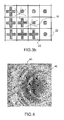
- the figure 3b is an enlargement of an example of a sudden break in periodicity. Indeed, some adjacent radiating elements, such as the elements 22 and 23, are very different from each other. At the transitions between two very different adjacent radiating elements, there is a discontinuity which induces a diffraction 19 of the radiation reflected by the reflector grating and an attenuation of the electromagnetic field radiated above the radiating surface.
- the figure 4 shows the attenuations 40 of the electromagnetic field obtained with the reflector network of the figure 3a .
- This figure 4 shows that there is a very clear correspondence between the intervals of periodicity of the radiating surface of the figure 3a and attenuations of the electromagnetic field radiated above this surface.
- This arrangement gives a disturbed radiation pattern with an increase in the level of the side lobes and does not allow to obtain a good directivity of the antenna comprising this reflector network.
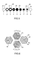
- the figure 5 represents an example of a semi-periodic pattern comprising a one-dimensional arrangement of a plurality of elementary radiating elements and making it possible to obtain a 360 ° phase rotation, according to the invention.
- the geometric shape of the radiating elements is hexagonal, their peripheral circumferential dimension is identical. They are made in planar technology and their radiating structure is not more complex than that of the radiating elements represented on the plate. figure 2 but said radiating structure evolves progressively from a radiating element to an adjacent radiating element, in the plane of the reflecting surface 14, and therefore does not exhibit a sudden rupture between two adjacent radiating elements.
- the first 1 and the last 9 radiating element are identical. This makes it possible to realize a phase variation loop of 360 ° since the final state is identical to the initial state.
- the first element 1 comprises a peripheral circumferential metal ring 26 delimiting an internal cavity 27.
- the following three consecutive elements 2, 3, 4 also comprise a peripheral circumferential metal ring 26 delimiting an internal cavity 27, the width of the ring progressively increasing from one radiating element to a second radiating element immediately adjacent to obtaining the fifth element 5, placed in the center of the pattern, which is a complete metal patch 25.
- the following consecutive radiating elements 7, 8 have a hexagonal slot 24 whose width increases progressively until the disappearance of the internal metal patch 25 as the radiating element 9.
- a change in the width or length of the slot, or the addition of a capacitive load has the effect of modifying the wave propagation characteristics in the slot and affecting the electrical length of the slot.
- the electrical length of a slot corresponds to its physical length relative to the wavelength that propagates there.
- a resonant cavity is formed between the metal patch and the metal ground plane.
- Part of the incident wave illuminating this radiating element is then transmitted to the metal ground plane of the radiating element which reflects the incident wave with a phase shift.
- the opening thus introduces a phase shift in the wave reflected by the radiating element which is all the more important as the opening is large.
- the maximum phase shift is obtained when the radiating element 1, 9 no longer comprises a metal patch but only a thin metal ring delimiting a resonant cavity.
- phase variation cycle such as that shown in FIG. figure 5 it is possible to obtain a phase shift greater than 360 °. For this, it suffices to repeat several times the same pattern of variation of the structure of the radiating elements.
- the number of radiating elements for make a pattern may be different from that of the figure 5 , but it is necessary enough so as not to create a sudden break in the periodicity of the reflecting surface 14.
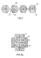
- a first element 50 consists of a complete metal patch, and each of the three following radiating elements 51, 52, 53 comprises three concentric hexagonal slots 54, 55, 56 made in a metal patch.
- the width of the slots, in the plane of the reflecting surface 14, increases between the second 51 and the third 52 element and then the width of the metal areas increases between the third 52 and the fourth 53 element.
- the radiating elements, in number of four on the figure 6 can be arranged according to the pattern shown in this example, this pattern can be reproduced recursively on the entire reflecting surface 14.
- the frequency of the incidence wave it is one or the other of the three slots of the patch that resonates.
- the widths of the three slots evolve simultaneously, but the invention is not limited to this case. It is also possible to produce a pattern comprising radiating elements in which the slots have widths that evolve independently of one another and / or radiating elements in which only one or two slots have a width which changes from one element radiating to another adjacent radiating element.
- the radiating elements having several slots in a metal patch make it possible to achieve a progression of the phase variation more elaborate than with elements having only one slot. They make it possible to obtain a range of phase variation up to 1000 ° and to reduce the number of transitions.
- the radiating elements have a hexagonal shape, but the same principle can be used for all types of geometric shapes, such as, for example, a square, rectangular, circular, triangular shape, a cross, or another form.
- the radiating elements comprising at least one slot, to gradually introduce one or more short circuits as described above in connection with the figure 7 or further in connection with the figure 8 .
- radiating elements comprise a patch 25 and a slot 24, or several slots, into which is introduced one or more short-circuits 28 for varying the electrical length of the slot.
- Short circuits 28 may be of the passive type when they consist of a simple metallization sectioning the slot 24 at a predetermined location and length to obtain at least two half-slots 24a and 24b of selected lengths.
- the short circuits can be of the active type when they are made by means of micro-switches, for example of the MEMS type (in English: Micro Electro-Mechanical System) or diodes.
- MEMS Micro Electro-Mechanical System
- radiators with multiple resonators coupled together in a reflector network thus makes it possible to considerably reduce the number of abrupt transitions in the reflector network and to reduce all the perturbations induced on the radiation pattern.
- Another advantage is that with a number of degrees of increased freedom, it is possible to guarantee the required phase shift not only at central frequency, but also at several other frequencies of the bandwidth of the reflector network.
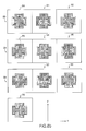
- the figure 8a shows an example of a radiating element in the shape of a cross with two perpendicular branches.
- the cross and the hexagon have the property of being miniature because the slits that determine the resonance are curved. This allows to insert several separate resonators on the metal patch and with four slots for example, it is possible to vary the phase up to 1000 ° without creating strong transitions.
- the cross has three concentric annular slots 81, 82, 83 made in a metal patch, but it could have a different number of three.
- the hexagon it is possible to progressively control the variation of the phase on a reflecting surface by arranging a plurality of cross-shaped radiating elements having varying slot widths or metal ring widths. .
- each cross may for example be inscribed inside a continuous metal grid 84 having a mesh of different geometric shape, for example square, rectangular or hexagonal.
- a continuous metal grid 84 having a mesh of different geometric shape, for example square, rectangular or hexagonal.
- MEMS type 85 In English: Micro Electro-Mechanical System
- other switching systems as diodes, arranged in a chosen manner in the slots as represented for example on the figures 8a and 8b .
- all the radiating elements have the same structure and all the annular slots have the same width.
- the MEMS 85 placed in the slots 81, 82, 83 have two possible states, open or closed, and act as a short circuit or as an open circuit.
- the pattern has ten identical cross-shaped radiating elements having three concentric annular slots and having the same number of MEMS, ie two MEMS paired along the Y axis, in the first innermost slot, six MEMS in the second slot, and six MEMS in the third outer slot.
- the six MEMS of the second, respectively third, slot are paired in pairs along the Y axis and the other four MEMS paired together.
- the first radiating element 90 all the MEMS are in a closed state.
- the four MEMS of the third slot that are paired together are in an open state, all other MEMS being in a closed state.
- the two MEMS of the first slot are in the open state and all the other MEMS are in the closed state.
- the following radiating elements 93 to 98 comprise other combinations of states of the different MEMS up to the last radiating element 99 of the pattern for which all MEMS are in the same closed state as the first radiating element of the pattern. Such a pattern makes it possible to vary the phase of the radiating elements by 360 °.
- the geometry of the radiating element figures 8a and 8b is in the shape of a cross, but alternatively MEMS can be placed in radiating elements having another geometry such as a hexagon, square, rectangle or any other desired shape.
- a radiating element in the shape of a cross or in the form of a hexagon has the advantage of being very compact and therefore broadband.
- a radiating element in the form of a cross makes it possible to obtain an antenna operating between 11 and 14 GHz.
- a cross shape has the advantage of being compatible with a square or rectangular mesh, which simplifies the production of a panel comprising a reflector network composed of radiating elements having this cross shape.
- radiating elements having one or more slots of scalable width and radiating elements having one or more slots having a scalable electrical length may include radiating elements having at least one slot passively short-circuited and / or radiating elements having at least one slot actively short-circuited and / or radiating elements having at least one slot incorporating capacitive MEMS.
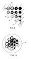
- FIG 9 illustrates an example of a database according to the invention.
- This database contains the radiating elements 1 to 9 of the figure 5 and additional radiating elements 63 to 68 having different intermediate structures. Using this database to correctly select the path of variation, it is possible to achieve a gradual variation of the phase of a reflected wave, from a gradual physical variation of the radiating elements. On this figure 9 different possible paths make it possible to obtain a progressive phase variation of 360 °. Two examples of paths 61, 62 are shown.
- phase variation obtained for a variation path such as the path 61 or 62, chosen in the database of the figure 9 , for an angle of incidence of the plane wave e equal to 30 ° and three different central frequencies, is represented on the figure 11 .
- the three frequencies of this example are 14 GHz, 14.25 GHz, 14.50 GHz and the phase variation obtained is between 60 ° and 420 ° for a pattern having 45 different radiating elements.
- This figure 11 shows a progressive phase variation that does not include a sudden jump.
- the database may be extended to radiating elements having a plurality of hexagonal slots. In this case, it becomes possible to achieve exactly the desired phase shift for the center frequency of the antenna radiation pattern as well as the desired phase dispersion.
- the radiating elements chosen to achieve a predetermined phase variation can then be arranged according to a two-dimensional reflective network as represented for example on the figure 10 .
- the reflective network thus produced makes it possible to obtain a progressive variation of the phase of the incident waves reflected by the network from a progressive physical variation of the elementary radiating elements of the network.
Landscapes
- Aerials With Secondary Devices (AREA)
- Variable-Direction Aerials And Aerial Arrays (AREA)
Applications Claiming Priority (1)
| Application Number | Priority Date | Filing Date | Title |
|---|---|---|---|
| FR0805530A FR2936906B1 (fr) | 2008-10-07 | 2008-10-07 | Reseau reflecteur a arrangement optimise et antenne comportant un tel reseau reflecteur |
Publications (2)
| Publication Number | Publication Date |
|---|---|
| EP2175523A1 true EP2175523A1 (de) | 2010-04-14 |
| EP2175523B1 EP2175523B1 (de) | 2019-06-12 |
Family
ID=40365390
Family Applications (1)
| Application Number | Title | Priority Date | Filing Date |
|---|---|---|---|
| EP09171108.5A Active EP2175523B1 (de) | 2008-10-07 | 2009-09-23 | Reflektor und Antenne die einen solchen Reflektor umfasst |
Country Status (9)
| Country | Link |
|---|---|
| US (1) | US8319698B2 (de) |
| EP (1) | EP2175523B1 (de) |
| JP (1) | JP5589225B2 (de) |
| KR (1) | KR101528938B1 (de) |
| CN (1) | CN101714695B (de) |
| CA (1) | CA2681548C (de) |
| ES (1) | ES2738531T3 (de) |
| FR (1) | FR2936906B1 (de) |
| RU (1) | RU2520370C2 (de) |
Cited By (4)
| Publication number | Priority date | Publication date | Assignee | Title |
|---|---|---|---|---|
| WO2010138731A1 (en) | 2009-05-29 | 2010-12-02 | Raytheon Company | Low loss variable phase reflect array using dual resonance phase-shifting element |
| EP2267843A1 (de) * | 2009-05-22 | 2010-12-29 | Korea Minting, Security Printing & ID Card Operating Corp. | Elektromagnetische Bandabstand-Musterstruktur, Herstellungsverfahren und Sicherheitsprodukt damit |
| FR2980044A1 (fr) * | 2011-09-14 | 2013-03-15 | Thales Sa | Cellule dephaseuse rayonnante reconfigurable basee sur des resonances fentes et microrubans complementaires |
| US20220085515A1 (en) * | 2018-12-28 | 2022-03-17 | Thales | Method for integrating a "network" antenna into a different electromagnetic medium, and associated antenna |
Families Citing this family (34)
| Publication number | Priority date | Publication date | Assignee | Title |
|---|---|---|---|---|
| US20040077604A1 (en) | 2001-12-19 | 2004-04-22 | Lenard Lichtenberger | Method and compositions employing formulations of lecithin oils and nsaids for protecting the gastrointestinal tract and providingenhanced therapeutic activity |
| JP5371633B2 (ja) * | 2008-09-30 | 2013-12-18 | 株式会社エヌ・ティ・ティ・ドコモ | リフレクトアレイ |
| JP5177708B2 (ja) | 2010-08-27 | 2013-04-10 | 株式会社エヌ・ティ・ティ・ドコモ | リフレクトアレイ |
| US8164532B1 (en) | 2011-01-18 | 2012-04-24 | Dockon Ag | Circular polarized compound loop antenna |
| EP2760433B1 (de) | 2011-09-29 | 2023-05-31 | PLx Opco Inc. | Ph-abhängige träger zur gezielten freisetzung von pharmazeutika entlang den gastrointestinaltrakts, zusammensetzungen daraus sowie ihre herstellung und verwendung |
| EP2882036B1 (de) * | 2012-07-31 | 2023-06-14 | Ntt Docomo, Inc. | Reflektionsanordnung |
| WO2014045273A1 (en) * | 2012-09-24 | 2014-03-27 | Convergent R.N.R Ltd | X-ray reflective lens arrangement |
| US20140085693A1 (en) * | 2012-09-26 | 2014-03-27 | Northeastern University | Metasurface nanoantennas for light processing |
| EP2905840B1 (de) * | 2012-10-01 | 2018-08-01 | NTT DoCoMo, Inc. | Reflektionsanordnung |
| CN103001005B (zh) * | 2012-10-25 | 2014-12-17 | 中兴通讯股份有限公司 | 降低电磁辐射比吸收率的装置及移动终端 |
| EP3014701A4 (de) * | 2013-07-16 | 2017-03-01 | Ramot at Tel-Aviv University Ltd. | Optischer collage-reflektionsarray |
| US10263342B2 (en) | 2013-10-15 | 2019-04-16 | Northrop Grumman Systems Corporation | Reflectarray antenna system |
| KR102175681B1 (ko) * | 2014-11-20 | 2020-11-06 | 삼성전자주식회사 | 재방사 중계기 |
| CN104733849B (zh) * | 2015-04-13 | 2018-05-08 | 南京肯微弗通信技术有限公司 | 反射阵辐射单元及平板反射阵天线 |
| US9812786B2 (en) * | 2015-08-25 | 2017-11-07 | Huawei Technologies Co., Ltd. | Metamaterial-based transmitarray for multi-beam antenna array assemblies |
| KR20180053200A (ko) * | 2016-11-11 | 2018-05-21 | 삼성전자주식회사 | 패턴이 형성된 거울을 포함하는 빔포밍 안테나 어셈블리와 이를 포함하는 차량 사이드 미러 어셈블리 |
| US11437731B2 (en) * | 2017-09-13 | 2022-09-06 | Metawave Corporation | Method and apparatus for a passive radiating and feed structure |
| KR101885659B1 (ko) * | 2017-10-20 | 2018-08-06 | 국방과학연구소 | 이득 및 부엽 재구성 가능한 반사판 안테나 |
| US10903568B2 (en) * | 2018-11-20 | 2021-01-26 | Nokia Technologies Oy | Electrochromic reflectarray antenna |
| US10944164B2 (en) | 2019-03-13 | 2021-03-09 | Northrop Grumman Systems Corporation | Reflectarray antenna for transmission and reception at multiple frequency bands |
| US11258182B2 (en) * | 2019-05-31 | 2022-02-22 | Metawave Corporation | Meta-structure based reflectarrays for enhanced wireless applications |
| US11476587B2 (en) * | 2019-06-14 | 2022-10-18 | City University Of Hong Kong | Dielectric reflectarray antenna and method for making the same |
| CN110600884B (zh) * | 2019-08-20 | 2020-07-07 | 南京理工大学 | 基于带有凹形臂的单层开槽贴片单元的宽带反射阵列天线 |
| CN112563761B (zh) * | 2019-09-25 | 2022-07-22 | 上海华为技术有限公司 | 一种天线装置及信号处理方法 |
| CN110649381B (zh) * | 2019-09-29 | 2021-06-22 | 厦门大学嘉庚学院 | 一种梯形多缝隙分形分裂生长式阵列天线 |
| US10892549B1 (en) | 2020-02-28 | 2021-01-12 | Northrop Grumman Systems Corporation | Phased-array antenna system |
| JP7290588B2 (ja) * | 2020-03-02 | 2023-06-13 | Kddi株式会社 | メタサーフェス反射板 |
| CN111555036B (zh) * | 2020-05-15 | 2022-09-30 | 中国航空工业集团公司沈阳飞机设计研究所 | 宽频梯度相位实现方法及超材料 |
| US12512607B2 (en) * | 2020-07-14 | 2025-12-30 | Boise State University | Millimeter wave reconfigurable antenna with single layered unit cell pattern |
| TWI744180B (zh) * | 2021-01-27 | 2021-10-21 | 國立中正大學 | 電磁波透射結構、電磁波透射結構陣列及電磁波透射偏移方法 |
| CN115000726B (zh) * | 2021-03-01 | 2025-02-28 | 华为技术有限公司 | 一种反射阵列天线及基站 |
| CN113078461B (zh) * | 2021-03-11 | 2022-05-13 | 重庆邮电大学 | 一种基于镜像对称法的反射阵列天线单元 |
| CN113823904B (zh) * | 2021-08-03 | 2022-12-09 | 清华大学 | 一种e波段高增益平面反射阵天线 |
| CN116526152B (zh) * | 2023-03-09 | 2025-01-28 | 浙江大学 | 一种宽带高增益的平面反射阵 |
Citations (4)
| Publication number | Priority date | Publication date | Assignee | Title |
|---|---|---|---|---|
| US4905014A (en) * | 1988-04-05 | 1990-02-27 | Malibu Research Associates, Inc. | Microwave phasing structures for electromagnetically emulating reflective surfaces and focusing elements of selected geometry |
| US20030058189A1 (en) * | 2001-09-27 | 2003-03-27 | Crouch David D. | Reflecting surfaces having geometries independent of geometries of wavefronts reflected therefrom |
| EP1796450A1 (de) * | 2004-09-06 | 2007-06-13 | Mitsubishi Gas Chemical Company, Inc. | Wellenabsorbierer |
| US20080024368A1 (en) * | 2006-07-28 | 2008-01-31 | Tatung Company | Microstrip reflectarray antenna |
Family Cites Families (21)
| Publication number | Priority date | Publication date | Assignee | Title |
|---|---|---|---|---|
| SU1022245A1 (ru) * | 1981-12-29 | 1983-06-07 | Предприятие П/Я В-8751 | Отражательна антенна решетка |
| RU2047250C1 (ru) * | 1983-04-13 | 1995-10-27 | Научно-исследовательский институт радиостроения | Способ изготовления поляризационного параболического антенного отражателя |
| US5543809A (en) * | 1992-03-09 | 1996-08-06 | Martin Marietta Corp. | Reflectarray antenna for communication satellite frequency re-use applications |
| JP3178428B2 (ja) * | 1998-09-04 | 2001-06-18 | 株式会社村田製作所 | 高周波放射源アレー、アンテナモジュールおよび無線装置 |
| US6020853A (en) * | 1998-10-28 | 2000-02-01 | Raytheon Company | Microstrip phase shifting reflect array antenna |
| US6538621B1 (en) * | 2000-03-29 | 2003-03-25 | Hrl Laboratories, Llc | Tunable impedance surface |
| US6384797B1 (en) * | 2000-08-01 | 2002-05-07 | Hrl Laboratories, Llc | Reconfigurable antenna for multiple band, beam-switching operation |
| US6396449B1 (en) * | 2001-03-15 | 2002-05-28 | The Boeing Company | Layered electronically scanned antenna and method therefor |
| FR2826511B1 (fr) | 2001-06-21 | 2003-12-19 | Cit Alcatel | Procede de repointage pour antenne reseau a reflecteur |
| FR2841389B1 (fr) | 2002-06-21 | 2004-09-24 | Thales Sa | Cellule dephaseuse pour reseau reflecteur d'antenne |
| FR2843238B1 (fr) | 2002-07-31 | 2006-07-21 | Cit Alcatel | Antenne multisources notamment pour un systeme a reflecteur |
| US7154451B1 (en) * | 2004-09-17 | 2006-12-26 | Hrl Laboratories, Llc | Large aperture rectenna based on planar lens structures |
| FR2860107B1 (fr) | 2003-09-23 | 2006-01-13 | Cit Alcatel | Antenne reseau reflecteur reconfigurable a faibles pertes |
| FR2866480B1 (fr) | 2004-02-17 | 2006-07-28 | Cit Alcatel | Dispositif rayonnant compact multipolarisation a alimentation orthogonale par ligne(s) a champ de surface |
| FR2868216B1 (fr) | 2004-03-23 | 2006-07-21 | Alcatel Sa | Cellule dephaseuse a polarisation lineaire et a longueur resonante variable au moyen de commutateurs mems |
| FR2874749B1 (fr) | 2004-08-31 | 2006-11-24 | Cit Alcatel | Antenne reseau reflecteur a zone de couverture de forme reconfigurable avec ou sans chargeur |
| US7920100B2 (en) * | 2005-08-18 | 2011-04-05 | Raytheon Company | Foldable reflect array |
| WO2007051487A1 (en) * | 2005-11-03 | 2007-05-10 | Centre National De La Recherche Scientifique (C.N.R.S.) | A reflectarry and a millimetre wave radar |
| CN1972015B (zh) * | 2005-11-22 | 2010-06-23 | 大同股份有限公司 | 可变槽孔尺寸的反射板 |
| FR2911011B1 (fr) | 2006-12-27 | 2010-08-27 | Alcatel Lucent | Antenne reseau rayonnant reconfigurable |
| US7872614B2 (en) * | 2007-10-31 | 2011-01-18 | Communications & Power Industries, Inc. | System and method for providing a deployable phasing structure |
-
2008
- 2008-10-07 FR FR0805530A patent/FR2936906B1/fr not_active Expired - Fee Related
-
2009
- 2009-09-23 EP EP09171108.5A patent/EP2175523B1/de active Active
- 2009-09-23 ES ES09171108T patent/ES2738531T3/es active Active
- 2009-09-28 CN CN200910174515.2A patent/CN101714695B/zh not_active Expired - Fee Related
- 2009-10-05 US US12/573,499 patent/US8319698B2/en active Active
- 2009-10-05 CA CA2681548A patent/CA2681548C/fr active Active
- 2009-10-06 JP JP2009232562A patent/JP5589225B2/ja not_active Expired - Fee Related
- 2009-10-06 RU RU2009137020/08A patent/RU2520370C2/ru active
- 2009-10-06 KR KR1020090094804A patent/KR101528938B1/ko not_active Expired - Fee Related
Patent Citations (4)
| Publication number | Priority date | Publication date | Assignee | Title |
|---|---|---|---|---|
| US4905014A (en) * | 1988-04-05 | 1990-02-27 | Malibu Research Associates, Inc. | Microwave phasing structures for electromagnetically emulating reflective surfaces and focusing elements of selected geometry |
| US20030058189A1 (en) * | 2001-09-27 | 2003-03-27 | Crouch David D. | Reflecting surfaces having geometries independent of geometries of wavefronts reflected therefrom |
| EP1796450A1 (de) * | 2004-09-06 | 2007-06-13 | Mitsubishi Gas Chemical Company, Inc. | Wellenabsorbierer |
| US20080024368A1 (en) * | 2006-07-28 | 2008-01-31 | Tatung Company | Microstrip reflectarray antenna |
Non-Patent Citations (2)
| Title |
|---|
| JOSÉ A ENCINAR: "Design of Two-Layer Printed Reflectarrays Using Patches of Variable Size", IEEE TRANSACTIONS ON ANTENNAS AND PROPAGATION, IEEE SERVICE CENTER, PISCATAWAY, NJ, US, vol. 49, no. 10, 1 October 2001 (2001-10-01), XP011004124, ISSN: 0018-926X * |
| SHA K ET AL: "Characteristics of new types of quasi-optical diplexers", ELECTRONICS & COMMUNICATIONS IN JAPAN, PART I - COMMUNICATIONS, WILEY, HOBOKEN, NJ, US, vol. 69, no. 12, 1 December 1986 (1986-12-01), pages 90 - 99, XP002141598, ISSN: 8756-6621 * |
Cited By (8)
| Publication number | Priority date | Publication date | Assignee | Title |
|---|---|---|---|---|
| EP2267843A1 (de) * | 2009-05-22 | 2010-12-29 | Korea Minting, Security Printing & ID Card Operating Corp. | Elektromagnetische Bandabstand-Musterstruktur, Herstellungsverfahren und Sicherheitsprodukt damit |
| WO2010138731A1 (en) | 2009-05-29 | 2010-12-02 | Raytheon Company | Low loss variable phase reflect array using dual resonance phase-shifting element |
| EP2436085A4 (de) * | 2009-05-29 | 2014-05-14 | Raytheon Co | Phasenvariable reflexionsanordnung mit geringem verlust sowie mit einem doppelten resonanzphasenverschiebungselement |
| FR2980044A1 (fr) * | 2011-09-14 | 2013-03-15 | Thales Sa | Cellule dephaseuse rayonnante reconfigurable basee sur des resonances fentes et microrubans complementaires |
| EP2571098A1 (de) * | 2011-09-14 | 2013-03-20 | Institut National des Sciences Appliquées de Rennes | Rekonfiguerierbare strahlende dephasierende Zelle, die auf Spaltresonanzen und komplementären Mikrostreifen basiert |
| US9647336B2 (en) | 2011-09-14 | 2017-05-09 | Thales | Reconfigurable radiating phase-shifting cell based on complementary slot and microstrip resonances |
| US20220085515A1 (en) * | 2018-12-28 | 2022-03-17 | Thales | Method for integrating a "network" antenna into a different electromagnetic medium, and associated antenna |
| US11646500B2 (en) * | 2018-12-28 | 2023-05-09 | Thales | Method for integrating a “network” antenna into a different electromagnetic medium, and associated antenna |
Also Published As
| Publication number | Publication date |
|---|---|
| CA2681548A1 (fr) | 2010-04-07 |
| RU2009137020A (ru) | 2011-04-20 |
| US8319698B2 (en) | 2012-11-27 |
| CA2681548C (fr) | 2017-03-21 |
| KR20100039264A (ko) | 2010-04-15 |
| JP5589225B2 (ja) | 2014-09-17 |
| RU2520370C2 (ru) | 2014-06-27 |
| ES2738531T3 (es) | 2020-01-23 |
| EP2175523B1 (de) | 2019-06-12 |
| CN101714695B (zh) | 2015-06-10 |
| CN101714695A (zh) | 2010-05-26 |
| KR101528938B1 (ko) | 2015-06-15 |
| JP2010093811A (ja) | 2010-04-22 |
| US20100085272A1 (en) | 2010-04-08 |
| FR2936906B1 (fr) | 2011-11-25 |
| FR2936906A1 (fr) | 2010-04-09 |
Similar Documents
| Publication | Publication Date | Title |
|---|---|---|
| EP2175523B1 (de) | Reflektor und Antenne die einen solchen Reflektor umfasst | |
| EP2564466B1 (de) | Kompaktes strahlungselement mit hohlraumresonatoren | |
| CA2793126C (fr) | Antenne reseau reflecteur a compensation de polarisation croisee et procede de realisation d'une telle antenne | |
| EP2571098B1 (de) | Rekonfiguerierbare strahlende dephasierende Zelle, die auf Spaltresonanzen und komplementären Mikrostreifen basiert | |
| CA2687161C (fr) | Element rayonnant planaire a polarisation duale et antenne reseau comportant un tel element rayonnant | |
| EP2795724B1 (de) | Basisantenne und entsprechende ein-oder zweidimensionale gruppenantenne | |
| EP2869400B1 (de) | Doppelpolarisierter kompakter Leistungsverteiler, Netz aus mehreren Verteilern, kompaktes Strahlungselement und Flachantenne, die einen solchen Verteiler umfasst | |
| EP2194602B1 (de) | Antenne mit gemeinsam benützten Elementarstrahlern und Verfahren zum Entwurf einer Mehrstrahlantenne mit gemeinsam benützten Elementarstrahlern | |
| CA2862729A1 (fr) | Formateur multi-faisceaux a deux dimensions, antenne comportant un tel formateur multi-faisceaux et systeme de telecommunication par satellite comportant une telle antenne | |
| EP2664030A1 (de) | Gedruckte schlitzrichtantenne und system mit einer gruppe aus bedruckten schlitzrichtantennen | |
| CA2460820C (fr) | Antenne a large bande ou multi-bandes | |
| CA2808511C (fr) | Antenne plane pour terminal fonctionnant en double polarisation circulaire, terminal aeroporte et systeme de telecommunication par satellite comportant au moins une telle antenne | |
| FR2901062A1 (fr) | Dispositif rayonnant a cavite(s) resonnante(s) a air a fort rendement de surface, pour une antenne reseau | |
| EP4391232A1 (de) | Weitwinkel-impedanzanpassungsvorrichtung für eine gruppenantenne mit strahlungselementen und verfahren zum entwurf einer solchen vorrichtung | |
| FR2952759A1 (fr) | Antenne a reflecteurs et reseau focal | |
| FR2981514A1 (fr) | Systeme antennaire a une ou plusieurs spirale(s) et reconfigurable |
Legal Events
| Date | Code | Title | Description |
|---|---|---|---|
| PUAI | Public reference made under article 153(3) epc to a published international application that has entered the european phase |
Free format text: ORIGINAL CODE: 0009012 |
|
| AK | Designated contracting states |
Kind code of ref document: A1 Designated state(s): AT BE BG CH CY CZ DE DK EE ES FI FR GB GR HR HU IE IS IT LI LT LU LV MC MK MT NL NO PL PT RO SE SI SK SM TR |
|
| AX | Request for extension of the european patent |
Extension state: AL BA RS |
|
| 17P | Request for examination filed |
Effective date: 20101004 |
|
| 17Q | First examination report despatched |
Effective date: 20101029 |
|
| STAA | Information on the status of an ep patent application or granted ep patent |
Free format text: STATUS: EXAMINATION IS IN PROGRESS |
|
| GRAP | Despatch of communication of intention to grant a patent |
Free format text: ORIGINAL CODE: EPIDOSNIGR1 |
|
| STAA | Information on the status of an ep patent application or granted ep patent |
Free format text: STATUS: GRANT OF PATENT IS INTENDED |
|
| INTG | Intention to grant announced |
Effective date: 20190109 |
|
| RIN1 | Information on inventor provided before grant (corrected) |
Inventor name: LEGAY, HERVE Inventor name: CHINIARD, RENAUD Inventor name: BRESCIANI, DANIELE Inventor name: GIRARD, ETIENNE |
|
| GRAS | Grant fee paid |
Free format text: ORIGINAL CODE: EPIDOSNIGR3 |
|
| GRAA | (expected) grant |
Free format text: ORIGINAL CODE: 0009210 |
|
| STAA | Information on the status of an ep patent application or granted ep patent |
Free format text: STATUS: THE PATENT HAS BEEN GRANTED |
|
| RAP1 | Party data changed (applicant data changed or rights of an application transferred) |
Owner name: THALES |
|
| AK | Designated contracting states |
Kind code of ref document: B1 Designated state(s): AT BE BG CH CY CZ DE DK EE ES FI FR GB GR HR HU IE IS IT LI LT LU LV MC MK MT NL NO PL PT RO SE SI SK SM TR |
|
| REG | Reference to a national code |
Ref country code: GB Ref legal event code: FG4D Free format text: NOT ENGLISH |
|
| REG | Reference to a national code |
Ref country code: CH Ref legal event code: EP |
|
| REG | Reference to a national code |
Ref country code: AT Ref legal event code: REF Ref document number: 1143817 Country of ref document: AT Kind code of ref document: T Effective date: 20190615 |
|
| REG | Reference to a national code |
Ref country code: DE Ref legal event code: R096 Ref document number: 602009058683 Country of ref document: DE |
|
| REG | Reference to a national code |
Ref country code: IE Ref legal event code: FG4D Free format text: LANGUAGE OF EP DOCUMENT: FRENCH |
|
| REG | Reference to a national code |
Ref country code: NL Ref legal event code: MP Effective date: 20190612 |
|
| REG | Reference to a national code |
Ref country code: LT Ref legal event code: MG4D |
|
| PG25 | Lapsed in a contracting state [announced via postgrant information from national office to epo] |
Ref country code: SE Free format text: LAPSE BECAUSE OF FAILURE TO SUBMIT A TRANSLATION OF THE DESCRIPTION OR TO PAY THE FEE WITHIN THE PRESCRIBED TIME-LIMIT Effective date: 20190612 Ref country code: LT Free format text: LAPSE BECAUSE OF FAILURE TO SUBMIT A TRANSLATION OF THE DESCRIPTION OR TO PAY THE FEE WITHIN THE PRESCRIBED TIME-LIMIT Effective date: 20190612 Ref country code: HR Free format text: LAPSE BECAUSE OF FAILURE TO SUBMIT A TRANSLATION OF THE DESCRIPTION OR TO PAY THE FEE WITHIN THE PRESCRIBED TIME-LIMIT Effective date: 20190612 Ref country code: NO Free format text: LAPSE BECAUSE OF FAILURE TO SUBMIT A TRANSLATION OF THE DESCRIPTION OR TO PAY THE FEE WITHIN THE PRESCRIBED TIME-LIMIT Effective date: 20190912 Ref country code: FI Free format text: LAPSE BECAUSE OF FAILURE TO SUBMIT A TRANSLATION OF THE DESCRIPTION OR TO PAY THE FEE WITHIN THE PRESCRIBED TIME-LIMIT Effective date: 20190612 |
|
| PG25 | Lapsed in a contracting state [announced via postgrant information from national office to epo] |
Ref country code: GR Free format text: LAPSE BECAUSE OF FAILURE TO SUBMIT A TRANSLATION OF THE DESCRIPTION OR TO PAY THE FEE WITHIN THE PRESCRIBED TIME-LIMIT Effective date: 20190913 Ref country code: LV Free format text: LAPSE BECAUSE OF FAILURE TO SUBMIT A TRANSLATION OF THE DESCRIPTION OR TO PAY THE FEE WITHIN THE PRESCRIBED TIME-LIMIT Effective date: 20190612 Ref country code: BG Free format text: LAPSE BECAUSE OF FAILURE TO SUBMIT A TRANSLATION OF THE DESCRIPTION OR TO PAY THE FEE WITHIN THE PRESCRIBED TIME-LIMIT Effective date: 20190912 |
|
| REG | Reference to a national code |
Ref country code: AT Ref legal event code: MK05 Ref document number: 1143817 Country of ref document: AT Kind code of ref document: T Effective date: 20190612 |
|
| REG | Reference to a national code |
Ref country code: ES Ref legal event code: FG2A Ref document number: 2738531 Country of ref document: ES Kind code of ref document: T3 Effective date: 20200123 |
|
| PG25 | Lapsed in a contracting state [announced via postgrant information from national office to epo] |
Ref country code: AT Free format text: LAPSE BECAUSE OF FAILURE TO SUBMIT A TRANSLATION OF THE DESCRIPTION OR TO PAY THE FEE WITHIN THE PRESCRIBED TIME-LIMIT Effective date: 20190612 Ref country code: EE Free format text: LAPSE BECAUSE OF FAILURE TO SUBMIT A TRANSLATION OF THE DESCRIPTION OR TO PAY THE FEE WITHIN THE PRESCRIBED TIME-LIMIT Effective date: 20190612 Ref country code: SK Free format text: LAPSE BECAUSE OF FAILURE TO SUBMIT A TRANSLATION OF THE DESCRIPTION OR TO PAY THE FEE WITHIN THE PRESCRIBED TIME-LIMIT Effective date: 20190612 Ref country code: CZ Free format text: LAPSE BECAUSE OF FAILURE TO SUBMIT A TRANSLATION OF THE DESCRIPTION OR TO PAY THE FEE WITHIN THE PRESCRIBED TIME-LIMIT Effective date: 20190612 Ref country code: PT Free format text: LAPSE BECAUSE OF FAILURE TO SUBMIT A TRANSLATION OF THE DESCRIPTION OR TO PAY THE FEE WITHIN THE PRESCRIBED TIME-LIMIT Effective date: 20191014 Ref country code: RO Free format text: LAPSE BECAUSE OF FAILURE TO SUBMIT A TRANSLATION OF THE DESCRIPTION OR TO PAY THE FEE WITHIN THE PRESCRIBED TIME-LIMIT Effective date: 20190612 Ref country code: NL Free format text: LAPSE BECAUSE OF FAILURE TO SUBMIT A TRANSLATION OF THE DESCRIPTION OR TO PAY THE FEE WITHIN THE PRESCRIBED TIME-LIMIT Effective date: 20190612 |
|
| PG25 | Lapsed in a contracting state [announced via postgrant information from national office to epo] |
Ref country code: SM Free format text: LAPSE BECAUSE OF FAILURE TO SUBMIT A TRANSLATION OF THE DESCRIPTION OR TO PAY THE FEE WITHIN THE PRESCRIBED TIME-LIMIT Effective date: 20190612 Ref country code: IS Free format text: LAPSE BECAUSE OF FAILURE TO SUBMIT A TRANSLATION OF THE DESCRIPTION OR TO PAY THE FEE WITHIN THE PRESCRIBED TIME-LIMIT Effective date: 20191012 |
|
| REG | Reference to a national code |
Ref country code: DE Ref legal event code: R097 Ref document number: 602009058683 Country of ref document: DE |
|
| PG25 | Lapsed in a contracting state [announced via postgrant information from national office to epo] |
Ref country code: TR Free format text: LAPSE BECAUSE OF FAILURE TO SUBMIT A TRANSLATION OF THE DESCRIPTION OR TO PAY THE FEE WITHIN THE PRESCRIBED TIME-LIMIT Effective date: 20190612 |
|
| PLBE | No opposition filed within time limit |
Free format text: ORIGINAL CODE: 0009261 |
|
| STAA | Information on the status of an ep patent application or granted ep patent |
Free format text: STATUS: NO OPPOSITION FILED WITHIN TIME LIMIT |
|
| PG25 | Lapsed in a contracting state [announced via postgrant information from national office to epo] |
Ref country code: PL Free format text: LAPSE BECAUSE OF FAILURE TO SUBMIT A TRANSLATION OF THE DESCRIPTION OR TO PAY THE FEE WITHIN THE PRESCRIBED TIME-LIMIT Effective date: 20190612 Ref country code: DK Free format text: LAPSE BECAUSE OF FAILURE TO SUBMIT A TRANSLATION OF THE DESCRIPTION OR TO PAY THE FEE WITHIN THE PRESCRIBED TIME-LIMIT Effective date: 20190612 |
|
| 26N | No opposition filed |
Effective date: 20200313 |
|
| PG25 | Lapsed in a contracting state [announced via postgrant information from national office to epo] |
Ref country code: IS Free format text: LAPSE BECAUSE OF FAILURE TO SUBMIT A TRANSLATION OF THE DESCRIPTION OR TO PAY THE FEE WITHIN THE PRESCRIBED TIME-LIMIT Effective date: 20200224 Ref country code: SI Free format text: LAPSE BECAUSE OF FAILURE TO SUBMIT A TRANSLATION OF THE DESCRIPTION OR TO PAY THE FEE WITHIN THE PRESCRIBED TIME-LIMIT Effective date: 20190612 Ref country code: MC Free format text: LAPSE BECAUSE OF FAILURE TO SUBMIT A TRANSLATION OF THE DESCRIPTION OR TO PAY THE FEE WITHIN THE PRESCRIBED TIME-LIMIT Effective date: 20190612 |
|
| REG | Reference to a national code |
Ref country code: CH Ref legal event code: PL |
|
| PG2D | Information on lapse in contracting state deleted |
Ref country code: IS |
|
| PG25 | Lapsed in a contracting state [announced via postgrant information from national office to epo] |
Ref country code: LI Free format text: LAPSE BECAUSE OF NON-PAYMENT OF DUE FEES Effective date: 20190930 Ref country code: CH Free format text: LAPSE BECAUSE OF NON-PAYMENT OF DUE FEES Effective date: 20190930 Ref country code: LU Free format text: LAPSE BECAUSE OF NON-PAYMENT OF DUE FEES Effective date: 20190923 Ref country code: IE Free format text: LAPSE BECAUSE OF NON-PAYMENT OF DUE FEES Effective date: 20190923 Ref country code: IS Free format text: LAPSE BECAUSE OF FAILURE TO SUBMIT A TRANSLATION OF THE DESCRIPTION OR TO PAY THE FEE WITHIN THE PRESCRIBED TIME-LIMIT Effective date: 20191112 |
|
| REG | Reference to a national code |
Ref country code: BE Ref legal event code: MM Effective date: 20190930 |
|
| PG25 | Lapsed in a contracting state [announced via postgrant information from national office to epo] |
Ref country code: BE Free format text: LAPSE BECAUSE OF NON-PAYMENT OF DUE FEES Effective date: 20190930 |
|
| PG25 | Lapsed in a contracting state [announced via postgrant information from national office to epo] |
Ref country code: CY Free format text: LAPSE BECAUSE OF FAILURE TO SUBMIT A TRANSLATION OF THE DESCRIPTION OR TO PAY THE FEE WITHIN THE PRESCRIBED TIME-LIMIT Effective date: 20190612 |
|
| PG25 | Lapsed in a contracting state [announced via postgrant information from national office to epo] |
Ref country code: MT Free format text: LAPSE BECAUSE OF FAILURE TO SUBMIT A TRANSLATION OF THE DESCRIPTION OR TO PAY THE FEE WITHIN THE PRESCRIBED TIME-LIMIT Effective date: 20190612 Ref country code: HU Free format text: LAPSE BECAUSE OF FAILURE TO SUBMIT A TRANSLATION OF THE DESCRIPTION OR TO PAY THE FEE WITHIN THE PRESCRIBED TIME-LIMIT; INVALID AB INITIO Effective date: 20090923 |
|
| PG25 | Lapsed in a contracting state [announced via postgrant information from national office to epo] |
Ref country code: MK Free format text: LAPSE BECAUSE OF FAILURE TO SUBMIT A TRANSLATION OF THE DESCRIPTION OR TO PAY THE FEE WITHIN THE PRESCRIBED TIME-LIMIT Effective date: 20190612 |
|
| PGFP | Annual fee paid to national office [announced via postgrant information from national office to epo] |
Ref country code: DE Payment date: 20250819 Year of fee payment: 17 |
|
| PGFP | Annual fee paid to national office [announced via postgrant information from national office to epo] |
Ref country code: IT Payment date: 20250827 Year of fee payment: 17 |
|
| PGFP | Annual fee paid to national office [announced via postgrant information from national office to epo] |
Ref country code: GB Payment date: 20250814 Year of fee payment: 17 |
|
| PGFP | Annual fee paid to national office [announced via postgrant information from national office to epo] |
Ref country code: FR Payment date: 20250821 Year of fee payment: 17 |
|
| PGFP | Annual fee paid to national office [announced via postgrant information from national office to epo] |
Ref country code: ES Payment date: 20251014 Year of fee payment: 17 |