EP2176644B1 - Dispositif de capteur microélectronique avec une source de lumière - Google Patents
Dispositif de capteur microélectronique avec une source de lumière Download PDFInfo
- Publication number
- EP2176644B1 EP2176644B1 EP08789335A EP08789335A EP2176644B1 EP 2176644 B1 EP2176644 B1 EP 2176644B1 EP 08789335 A EP08789335 A EP 08789335A EP 08789335 A EP08789335 A EP 08789335A EP 2176644 B1 EP2176644 B1 EP 2176644B1
- Authority
- EP
- European Patent Office
- Prior art keywords
- laser
- carrier
- light beam
- light source
- sensor device
- Prior art date
- Legal status (The legal status is an assumption and is not a legal conclusion. Google has not performed a legal analysis and makes no representation as to the accuracy of the status listed.)
- Not-in-force
Links
- 238000004377 microelectronic Methods 0.000 title claims description 22
- 230000003287 optical effect Effects 0.000 claims description 36
- 239000002245 particle Substances 0.000 claims description 25
- 238000000034 method Methods 0.000 claims description 23
- 239000000523 sample Substances 0.000 claims description 18
- 230000010355 oscillation Effects 0.000 claims description 10
- 239000000126 substance Substances 0.000 claims description 5
- 238000004458 analytical method Methods 0.000 claims description 4
- 230000001427 coherent effect Effects 0.000 claims description 4
- 239000012472 biological sample Substances 0.000 claims description 2
- 238000001514 detection method Methods 0.000 description 11
- 238000005259 measurement Methods 0.000 description 11
- 238000003556 assay Methods 0.000 description 6
- 230000000694 effects Effects 0.000 description 6
- 230000003993 interaction Effects 0.000 description 5
- 239000006249 magnetic particle Substances 0.000 description 5
- 238000001228 spectrum Methods 0.000 description 5
- 241000700605 Viruses Species 0.000 description 4
- 239000011324 bead Substances 0.000 description 4
- 230000008859 change Effects 0.000 description 4
- 238000010586 diagram Methods 0.000 description 4
- 239000012530 fluid Substances 0.000 description 4
- 239000011521 glass Substances 0.000 description 4
- 238000010438 heat treatment Methods 0.000 description 4
- 238000011835 investigation Methods 0.000 description 4
- 238000012360 testing method Methods 0.000 description 4
- 230000008901 benefit Effects 0.000 description 3
- 238000004166 bioassay Methods 0.000 description 3
- 238000006243 chemical reaction Methods 0.000 description 3
- 244000005700 microbiome Species 0.000 description 3
- 230000009467 reduction Effects 0.000 description 3
- 239000012780 transparent material Substances 0.000 description 3
- XLYOFNOQVPJJNP-UHFFFAOYSA-N water Substances O XLYOFNOQVPJJNP-UHFFFAOYSA-N 0.000 description 3
- 239000004793 Polystyrene Substances 0.000 description 2
- 238000013459 approach Methods 0.000 description 2
- 239000000969 carrier Substances 0.000 description 2
- 238000001816 cooling Methods 0.000 description 2
- 238000013461 design Methods 0.000 description 2
- 238000007641 inkjet printing Methods 0.000 description 2
- 239000000463 material Substances 0.000 description 2
- 238000012544 monitoring process Methods 0.000 description 2
- 229920003023 plastic Polymers 0.000 description 2
- 229920002223 polystyrene Polymers 0.000 description 2
- 230000008569 process Effects 0.000 description 2
- 210000003296 saliva Anatomy 0.000 description 2
- 239000004065 semiconductor Substances 0.000 description 2
- 108091034117 Oligonucleotide Proteins 0.000 description 1
- 239000012491 analyte Substances 0.000 description 1
- 239000006117 anti-reflective coating Substances 0.000 description 1
- 238000010256 biochemical assay Methods 0.000 description 1
- 239000008280 blood Substances 0.000 description 1
- 210000004369 blood Anatomy 0.000 description 1
- 239000011248 coating agent Substances 0.000 description 1
- 238000000576 coating method Methods 0.000 description 1
- 239000012141 concentrate Substances 0.000 description 1
- 230000003247 decreasing effect Effects 0.000 description 1
- 230000001419 dependent effect Effects 0.000 description 1
- 230000001066 destructive effect Effects 0.000 description 1
- 238000011161 development Methods 0.000 description 1
- 238000006073 displacement reaction Methods 0.000 description 1
- 239000003814 drug Substances 0.000 description 1
- 229940079593 drug Drugs 0.000 description 1
- 238000007824 enzymatic assay Methods 0.000 description 1
- 238000011156 evaluation Methods 0.000 description 1
- 230000005281 excited state Effects 0.000 description 1
- 238000002474 experimental method Methods 0.000 description 1
- 238000004186 food analysis Methods 0.000 description 1
- 238000004374 forensic analysis Methods 0.000 description 1
- 238000003384 imaging method Methods 0.000 description 1
- 238000002347 injection Methods 0.000 description 1
- 239000007924 injection Substances 0.000 description 1
- 230000002452 interceptive effect Effects 0.000 description 1
- 150000002500 ions Chemical class 0.000 description 1
- 239000007788 liquid Substances 0.000 description 1
- 238000012986 modification Methods 0.000 description 1
- 230000004048 modification Effects 0.000 description 1
- 230000000704 physical effect Effects 0.000 description 1
- 239000002861 polymer material Substances 0.000 description 1
- 238000002360 preparation method Methods 0.000 description 1
- 238000012545 processing Methods 0.000 description 1
- 230000002035 prolonged effect Effects 0.000 description 1
- 230000001902 propagating effect Effects 0.000 description 1
- 238000005086 pumping Methods 0.000 description 1
- -1 saliva Substances 0.000 description 1
- 238000005070 sampling Methods 0.000 description 1
- 238000007493 shaping process Methods 0.000 description 1
- 230000003595 spectral effect Effects 0.000 description 1
- 239000000758 substrate Substances 0.000 description 1
- 230000000007 visual effect Effects 0.000 description 1
- 238000005406 washing Methods 0.000 description 1
Images

Classifications
-
- G—PHYSICS
- G01—MEASURING; TESTING
- G01N—INVESTIGATING OR ANALYSING MATERIALS BY DETERMINING THEIR CHEMICAL OR PHYSICAL PROPERTIES
- G01N21/00—Investigating or analysing materials by the use of optical means, i.e. using sub-millimetre waves, infrared, visible or ultraviolet light
- G01N21/17—Systems in which incident light is modified in accordance with the properties of the material investigated
- G01N21/55—Specular reflectivity
- G01N21/552—Attenuated total reflection
-
- G—PHYSICS
- G01—MEASURING; TESTING
- G01N—INVESTIGATING OR ANALYSING MATERIALS BY DETERMINING THEIR CHEMICAL OR PHYSICAL PROPERTIES
- G01N21/00—Investigating or analysing materials by the use of optical means, i.e. using sub-millimetre waves, infrared, visible or ultraviolet light
- G01N21/62—Systems in which the material investigated is excited whereby it emits light or causes a change in wavelength of the incident light
- G01N21/63—Systems in which the material investigated is excited whereby it emits light or causes a change in wavelength of the incident light optically excited
- G01N21/64—Fluorescence; Phosphorescence
- G01N21/645—Specially adapted constructive features of fluorimeters
- G01N21/648—Specially adapted constructive features of fluorimeters using evanescent coupling or surface plasmon coupling for the excitation of fluorescence
-
- G—PHYSICS
- G01—MEASURING; TESTING
- G01N—INVESTIGATING OR ANALYSING MATERIALS BY DETERMINING THEIR CHEMICAL OR PHYSICAL PROPERTIES
- G01N27/00—Investigating or analysing materials by the use of electric, electrochemical, or magnetic means
- G01N27/72—Investigating or analysing materials by the use of electric, electrochemical, or magnetic means by investigating magnetic variables
- G01N27/74—Investigating or analysing materials by the use of electric, electrochemical, or magnetic means by investigating magnetic variables of fluids
- G01N27/745—Investigating or analysing materials by the use of electric, electrochemical, or magnetic means by investigating magnetic variables of fluids for detecting magnetic beads used in biochemical assays
-
- G—PHYSICS
- G01—MEASURING; TESTING
- G01N—INVESTIGATING OR ANALYSING MATERIALS BY DETERMINING THEIR CHEMICAL OR PHYSICAL PROPERTIES
- G01N2201/00—Features of devices classified in G01N21/00
- G01N2201/06—Illumination; Optics
- G01N2201/064—Stray light conditioning
-
- G—PHYSICS
- G01—MEASURING; TESTING
- G01N—INVESTIGATING OR ANALYSING MATERIALS BY DETERMINING THEIR CHEMICAL OR PHYSICAL PROPERTIES
- G01N2201/00—Features of devices classified in G01N21/00
- G01N2201/06—Illumination; Optics
- G01N2201/069—Supply of sources
- G01N2201/0691—Modulated (not pulsed supply)
-
- G—PHYSICS
- G01—MEASURING; TESTING
- G01N—INVESTIGATING OR ANALYSING MATERIALS BY DETERMINING THEIR CHEMICAL OR PHYSICAL PROPERTIES
- G01N2201/00—Features of devices classified in G01N21/00
- G01N2201/06—Illumination; Optics
- G01N2201/069—Supply of sources
- G01N2201/0696—Pulsed
Definitions
- the invention relates to a microelectronic sensor device and a method for optical examinations at a carrier with the help of a light source. Moreover, it relates to the use of such a device.
- the US 2005/0048599 A1 discloses a method for the investigation of microorganisms that are tagged with particles such that a (e.g. magnetic) force can be exerted on them.
- a laser beam is directed through a transparent material to a surface where it is totally internally reflected.
- Light of this beam that leaves the transparent material as an evanescent wave is scattered by microorganisms and/or other components at the surface and then detected by a photodetector or used to illuminate the microorganisms for visual observation.
- a problem of this and similar setups is that interferences of the emitted laser light with reflections of this light may occur that change over time and thus cause undesired variations of the laser light output.
- the US 5 313 448 discloses an optical system comprising a laser light source for directing light onto a rotating disk. To prevent interference of reflected light pulses with light generation in the laser, the timing of the laser pulses is adjusted such that returning light arrives at the laser device when this is off.
- the microelectronic sensor device serves for optical examinations at a carrier, wherein the carrier does not necessarily belong to the device.
- the carrier will usually be made from a transparent material, for example glass or polystyrene, to allow the propagation of light of a given spectrum. Its concrete design depends on the application it is intended for. Moreover, it should be noted that the term “examination” is to be understood in a broad sense, comprising any kind of manipulation and/or interaction of light with some entity in or at the carrier.
- the examinations may preferably comprise the qualitative or quantitative detection of target components comprising label particles, wherein the target components may for example be biological substances like biomolecules, complexes, cell fractions or cells.
- the microelectronic sensor device comprises the following components:
- the invention further relates to a method for optical examinations at a carrier, comprising:
- the described microelectronic sensor device and method have the advantage to provide an input light beam which has a smaller feedback with reflections from the entrance window or other components of e.g. the carrier. With the reduction of this feedback, also variations of the feedback are reduced which may occur for example from slight dimensional changes of the optical components under thermal expansion.
- the modulation is a priori designed in so far as it comprises a pulsed emission of the input light beam, i.e. in that the input light beam consists of a series of pulses separated in time by pauses.
- the pulses may all be different from each other or, preferably, all have (approximately) the same shape.
- the emitted pulses of the light source may optionally be dimensioned such that they do not coincide in the light source with previous pulses of the light source that were reflected at the entrance window or other components of e.g. the carrier.
- the pulses that are reflected at e.g. the entrance window will not have any possibility of interference.
- the pulses are therefore designed such that a (e.g. first) relaxation minimum of a currently emitted pulse coincides in the laser light source (or, more precisely, in its internal laser cavity) with a (e.g. first) relaxation maximum of a previous pulse that was reflected at the entrance window or another component of the carrier.
- a relaxation minimum of a currently emitted pulse coincides in the laser light source (or, more precisely, in its internal laser cavity) with a (e.g. first) relaxation maximum of a previous pulse that was reflected at the entrance window or another component of the carrier.
- timing of the laser pulses is such that the first relaxation oscillation maximum of the externally reflected pulse number (N-1) coincides with the first relaxation minimum of the currently emitted pulse number N, then the laser is rather insensitive to this optical feedback due to a depletion of the carriers in the laser device at that time instance.
- the mentioned pulses of the input light beam are periodically repeated with a repetition frequency that ranges between approximately 100 MHz and 1 GHz. Additionally or alternatively, it is preferred that the pulses have a duty cycle which ranges between 1 % and 80 % (wherein this percentage indicates the fraction of time of the period during which the pulse is "on” in contrast to the pause or "off” time). It should be noted that, if extreme short optical pulses are generated by e.g. exciting only the first relaxation oscillation of a laser, this requires an electrical addressing scheme with pulse widths in the nsec regime, regardless of modulation frequency. For a modulation with a frequency of less than 10 MHz, the 1 nsec pulse width will then imply duty cycles lower than 1%.
- the laser current that drives a laser light source is modulated for introducing sidemodes into the input light beam and for making it less coherent.
- any constructive/destructive interference effects inside the laser can be prevented that may depend on the external cavity length (which is a rather optical effect).
- the carrier comprises a contact surface at which the input light beam is totally internally reflected as an output light beam.
- the contact surface must comprise an interface between two media, e.g. glass and water, at which total internal reflection (TIR) can take place if the incident light beam hits the interface at an appropriate angle (larger than the associated critical angle of TIR).
- TIR total internal reflection
- Such a setup is often used to examine small volumes of a sample at the TIR-interface which are probed by a non-propagating evanescent wave that is exponentially decaying into the medium with the lower refractive index (e.g. water).
- Target components - e.g.
- the output light beam of the sensor device will consist of the reflected light of the input light beam, wherein the small amount of light missing due to scattering of evanescent waves contains the desired information about the target components at the contact surface.
- a light detector for determining the amount of light in the output light beam (e.g. expressed as the intensity in the cross section of the beam).
- the detector may comprise any suitable sensor or plurality of sensors by which light of a given spectrum can be detected, for example photodiodes, photo resistors, photocells, a CCD chip, or a photo multiplier tube.
- the microelectronic sensor device comprises an actuator for manipulating target particles in a sample chamber adjacent to the carrier.
- the target particles may particularly be magnetic particles that can be moved by a magnetic field and thus deliberately be attracted to the contact surface of the carrier and/or washed away from it.
- the actuator will in this case usually comprise an electromagnet or a plurality of electromagnets.
- the operation of such an electromagnet or in general of an electrically driven actuator) will typically dissipate heat that induces thermal expansion of the surrounding components. This may cause uncontrollable and unpredictable variations in the interference of reflected light beams with the light source.
- disturbances due to said variations are much less critical.
- the invention further relates to the use of the microelectronic device described above for molecular diagnostics, biological sample analysis, or chemical sample analysis, food analysis, and/or forensic analysis.
- Molecular diagnostics may for example be accomplished with the help of magnetic beads or fluorescent particles that are directly or indirectly attached to target molecules.
- Figure 1 shows a general setup with a microelectronic sensor device according to the present invention.
- a central component of this setup is the carrier 11 that may for example be made from glass or transparent plastic like polystyrene.
- the carrier 11 is located next to a sample chamber 2 in which a sample fluid with target components to be detected (e.g. drugs, antibodies, DNA, etc.) can be provided.
- the sample further comprises magnetic particles, for example superparamagnetic beads, wherein these particles are usually bound as labels to the aforementioned target components.
- target particle 1 For simplicity only the combination of target components and magnetic particles is shown in the Figure and will be called "target particle 1" in the following.
- target particle 1 instead of magnetic particles other label particles, for example electrically charged or fluorescent particles, could be used as well.
- the interface between the carrier 11 and the sample chamber 2 is formed by a surface called "contact surface” 12.
- This contact surface 12 is coated with capture elements, e.g. antibodies, which can specifically bind the target particles.
- the sensor device comprises a magnetic field generator 41, for example an electromagnet with a coil and a core, for controllably generating a magnetic field at the contact surface 12 and in the adjacent space of the sample chamber 2.
- a magnetic field generator 41 for example an electromagnet with a coil and a core, for controllably generating a magnetic field at the contact surface 12 and in the adjacent space of the sample chamber 2.
- the target particles 1 can be manipulated, i.e. be magnetized and particularly be moved (if magnetic fields with gradients are used).
- an additional magnetic field generator can be incorporated at different positions, e.g. opposite to the shown magnetic field generator 41 at the other end of the contact surface 12, e.g. to wash unbound target particles away from the contact surface after an attraction phase during measurement.
- the sensor device further comprises a light source 21 that generates an input light beam L1 which is transmitted into the carrier 11 through an "entrance window" 14.
- a collimator lens may be used to make the input light beam L1 parallel, and a pinhole of e.g. 0.5 mm may be used to reduce the beam diameter.
- the input light beam L1 arrives at the contact surface 12 at an angle larger than the critical angle ⁇ c of total internal reflection (TIR) and is therefore totally internally reflected in an "output light beam” L2.
- TIR critical angle
- the output light beam L2 leaves the carrier 11 through another surface (“exit window” 15) and is detected by a light detector 31.
- the light detector 31 determines the amount of light of the output light beam L2 (e.g. expressed by the light intensity of this light beam in the whole spectrum or a certain part of the spectrum).
- the measured sensor signals S are evaluated and optionally monitored over an observation period by an evaluation and recording module 32 that is coupled to the detector 31.
- the detector 31 also for the sampling of fluorescence light emitted by fluorescent particles 1 which were stimulated by the input light beam L1, wherein this fluorescence may for example spectrally be discriminated from reflected light L2.
- this fluorescence may for example spectrally be discriminated from reflected light L2.
- the described microelectronic sensor device applies optical means for the detection of target particles 1.
- the detection technique should be surface-specific. As indicated above, this is achieved by using the principle of frustrated total internal reflection. This principle is based on the fact that an evanescent wave decays (exponentially dropping) into the sample 2 when the incident light beam L1 is totally internally reflected. If this evanescent wave then interacts with another medium like the bound target particles 1, part of the input light will be coupled into the sample fluid (this is called "frustrated total internal reflection") or will be absorbed by the target molecules and/or label particles (e.g.
- the reflected intensity will be reduced (while the reflected intensity will be 100% for a clean interface and no interaction).
- the amount of disturbance i.e. the amount of target particles on or very near (within about 200 nm) to the TIR surface (not in the rest of the sample chamber 2)
- the reflected intensity will drop accordingly. This intensity drop is a direct measure for the amount of bound target particles 1, and therefore for the concentration of target particles in the sample.
- the described procedure is independent of applied magnetic fields. This allows real-time optical monitoring of preparation, measurement and washing steps.
- the monitored signals can also be used to control the measurement or the individual process steps.
- medium A of the carrier 11 can be glass and/or some transparent plastic with a typical refractive index of 1.52.
- a particular advantage of the laser light source 21 that is used in the microelectronic sensor device of Figure 1 is that a nice narrow collimated input light beam L1 can be generated to illuminate a small investigation region 13 on the contact surface 12 where the bioassay takes place. Furthermore, the laser emits light of only one wavelength, which exactly determines the angle at which total internal reflection occurs in the carrier 11. However, due to the coherence of the laser light, problems may arise as a result of optical feedback when the dimensions of the cartridge slightly change due to temperature changes. These aspects will now be discussed in more detail.
- the (disposable) cartridge comprising the carrier 11 will usually consist of only simple, cheap injection molded parts, and it would be too expensive to apply antireflective coatings to the relevant surfaces of the carrier (entrance and exit window 14, 15).
- some part L1' of the input light beam L1 will be reflected from the entrance window 14 back into the laser (actually, a small - unwanted - interferometer is formed in this way).
- This will cause laser feedback, caused by the interference of the reflected light beam L1' in the laser cavity. Normally, this will not be a problem, as the effect is constant, and the introduced noise in the laser output is averaged out easily.
- electrical components like particularly the magnetic field generator 41 are present.
- the electromagnet 41 When the electromagnet 41 is switched on, it will dissipate heat, which will heat up the cartridge with the carrier 11 and the microelectronic sensor device itself. Now, there is a problem: due to the heating, the distance between the light source 21 and the carrier 11 can change up to several laser wavelengths (>> 1/10 ⁇ ), thereby influencing the laser feedback and causing intensity and noise irregularities in the laser output. The heating and cooling of the cartridge-reader ensemble usually takes up to 1 minute. During this time, the laser output will fluctuate, due to the continuously changing laser feedback. Also the signal from a possible forward sense diode, which may be located in the housing of the light source 21, will be influenced.
- laser modulator 22 which supplies the laser current to the light source 21 and which is set at a proper frequency (such modulators are often used in e.g. DVD players). Modulating the laser current of the laser device causes sidemodes to appear in the optical spectrum, making the laser less coherent and consequently less sensitive for optical feedback. Furthermore, laser feedback can be eliminated to a high extent by ensuring that a reflected wave and an emitted laser pulse do not coincide inside the laser diode at the same time.
- a constant laser output can be maintained (and misbehavior of a forward sense diode that may be incorporated inside the laser diode can be prevented) when the optical path length is changed slightly, e.g. due to heating of the cartridge and reader during magnetic actuation.
- the laser modulator 22 can particularly switch the laser on and off at a high frequency, in the order of a few hundred MHz. It may be set in such a way that:
- Figure 2 illustrates the effect of the described laser modulation.
- the diagram shows (for a selected point inside the laser cavity) a currently generated pulse P N and an interfering reflected previous pulse P N-1 ' (vertical axis: intensity I; horizontal axis: time t).
- the output of the laser shows fluctuations of the intensity I at the onset of the laser pulse due to the well known relaxation oscillations of laser diodes. If timing of the laser pulses is such that the first relaxation oscillation maximum of the externally reflected pulse P N-1 ' coincides with the first relaxation minimum in the currently emitted pulse P N (dashed line), the laser is rather insensitive to this optical feedback, due to a depletion of the carriers in the laser device at that time instance.
- the cavity roundtrip time is less than 1 ns. If the laser pulse duration is in the order of 1 ns or more (typical for a few hundred MHz modulation frequency), the front end of a laser pulse P N is already reflected back at the laser, whereas the end of the same pulse is still being emitted. In this case an emitted laser pulse P N can only be influenced by its preceding pulse P N-1 ' after this preceding pulse has traveled back and forth several times in the external laser cavity. In this case, by tuning the modulation frequency, the first relaxation maximum of pulse P N-1 ' can be brought into overlap (in time domain) with the first relaxation minimum of pulse P N .
- an emitted laser pulse is always reflected back into the laser while it is still being emitted.
- Decreased noise due to optical feedback can then only be achieved by modulating the laser current, thereby introducing spectral sidemodes and making the laser incoherent.
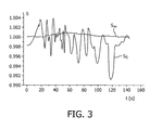
- Figure 3 shows in a diagram the recorded normalized optical signal S (vertical axis) that is measured by the light detector 31 over time t (horizontal axis) when an empty cartridge is put in the microelectronic sensor device and when the actuation magnet 41 is switched on for 20 seconds. Ideally, the signal should not change, as there is no bioassay inside the cartridge.
- the diagram shows two curves:
- the output light beam L2 that hits the light detector 31 will partly be reflected from the detector back to the carrier 11. Some of this light will be transmitted back to the light source 21, and some light will be reflected back to the detector. This will cause some interference effects on both the detector as on the laser side.
- the use of a modulator 22 can prevent these things to occur (however, setting the light detector 31 at an angle with respect to the incoming output light beam L2 will also largely resolve these phenomena).
- a modulator 22 not only compensates for expansion/shrinkage of the cartridge. Also other influences that alter the optical path length can be compensated for, e.g. small movements or tiltings of the cartridge during a measurement.
Landscapes
- Chemical & Material Sciences (AREA)
- Health & Medical Sciences (AREA)
- General Health & Medical Sciences (AREA)
- Life Sciences & Earth Sciences (AREA)
- Analytical Chemistry (AREA)
- Biochemistry (AREA)
- Physics & Mathematics (AREA)
- General Physics & Mathematics (AREA)
- Immunology (AREA)
- Pathology (AREA)
- Chemical Kinetics & Catalysis (AREA)
- Electrochemistry (AREA)
- Nuclear Medicine, Radiotherapy & Molecular Imaging (AREA)
- Investigating Or Analysing Materials By Optical Means (AREA)
- Investigating, Analyzing Materials By Fluorescence Or Luminescence (AREA)
Claims (8)
- Dispositif capteur micro-électronique pour examen optique au niveau d'un support (11), comprenant :a) une source de lumière (21) comprenant un laser pour émettre un faisceau de lumière d'entrée (L1) par l'intermédiaire d'une fenêtre d'entrée (14) dans le support (11);b) un modulateur (22) pour moduler la source de lumière (21) de manière à réduire des interférences optiques de la source de lumière (21) avec des reflets (L1') du faisceau de lumière d'entrée (L1) provenant de la fenêtre d'entrée (14) ou d'autres composants du support (11);dans lequel la modulation comprend une émission pulsée du faisceau de lumière d'entrée (L1),
caractérisé en ce qu'un minimum d'oscillation de relâchement d'une impulsion actuellement émise (PN) coïncide dans la source de lumière (21) avec un maximum d'oscillation de relâchement d'une impulsion précédente (PN-1') réfléchie à la fenêtre d'entrée (14) ou à d'autres composants du support (11) de retour dans le laser. - Procédé d'examens optiques au niveau d'un support (11), comprenant :a) l'émission, avec une source de lumière (21) comprenant un laser, d'un faisceau de lumière d'entrée (L1) par l'intermédiaire d'une fenêtre d'entrée (14) dans le support (11) ;b) la modulation de la source de lumière (21) avec un modulateur laser (22) de manière à réduire des interférences optiques de la source de lumière (21) avec des reflets (L1') du faisceau de lumière d'entrée (L1) engendrés par des changements de dimensions d'une cartouche (11) en provenance de la fenêtre d'entrée (14) ou d'autres composants du support (11) ;dans lequel la modulation comprend une émission pulsée du faisceau de lumière d'entrée (L1),
caractérisé en ce qu'un minimum d'oscillation de relâchement d'une impulsion actuellement émise (PN) coïncide dans la source de lumière (21) avec un maximum d'oscillation de relâchement d'une impulsion précédente (PN-1') réfléchie à la fenêtre d'entrée (14) ou à d'autres composants du support (11) de retour dans le laser. - Dispositif capteur micro-électronique selon la revendication 1 ou procédé selon la revendication 2,
caractérisé en ce que les impulsions (PN) du faisceau de lumière d'entrée (L1) ont une fréquence de répétition entre environ 100 MHz et 1 GHz, et/ou en ce qu'elles ont un rapport cyclique entre environ 1 % et 80 %. - Dispositif capteur micro-électronique selon la revendication 1 ou procédé selon la revendication 2,
caractérisé en ce que le courant laser qui commande la source de lumière (21) est modulé pour introduire des modes latéraux dans le faisceau de lumière d'entrée (L1) et pour le rendre moins cohérent. - Dispositif capteur micro-électronique selon la revendication 1 ou procédé selon la revendication 2,
caractérisé en ce que le support (11) comprend une surface de contact (12) à laquelle le faisceau de lumière d'entrée (L1) est totalement réfléchi en interne sous forme d'un faisceau de lumière de sortie (L2). - Dispositif capteur micro-électronique ou procédé selon la revendication 5,
caractérisé en ce que le faisceau de lumière de sortie (L2) est détecté avec un détecteur de lumière (31). - Dispositif capteur micro-électronique selon la revendication 1 ou procédé selon la revendication 2,
caractérisé en ce qu'il comprend un actionneur pour manipuler des particules cibles (1) dans une chambre d'échantillon (2) adjacente au support (11), particulièrement au moins un électroaimant (41). - Utilisation du dispositif capteur micro-électronique selon l'une quelconque des revendications 1 à 7 pour des diagnostics moléculaires, des analyses d'échantillons biologiques ou des analyses d'échantillons chimiques.
Priority Applications (1)
| Application Number | Priority Date | Filing Date | Title |
|---|---|---|---|
| EP08789335A EP2176644B1 (fr) | 2007-07-31 | 2008-07-17 | Dispositif de capteur microélectronique avec une source de lumière |
Applications Claiming Priority (3)
| Application Number | Priority Date | Filing Date | Title |
|---|---|---|---|
| EP07113478 | 2007-07-31 | ||
| PCT/IB2008/052869 WO2009016533A2 (fr) | 2007-07-31 | 2008-07-17 | Dispositif de capteur microélectronique avec une source de lumière |
| EP08789335A EP2176644B1 (fr) | 2007-07-31 | 2008-07-17 | Dispositif de capteur microélectronique avec une source de lumière |
Publications (2)
| Publication Number | Publication Date |
|---|---|
| EP2176644A2 EP2176644A2 (fr) | 2010-04-21 |
| EP2176644B1 true EP2176644B1 (fr) | 2012-10-31 |
Family
ID=40227558
Family Applications (1)
| Application Number | Title | Priority Date | Filing Date |
|---|---|---|---|
| EP08789335A Not-in-force EP2176644B1 (fr) | 2007-07-31 | 2008-07-17 | Dispositif de capteur microélectronique avec une source de lumière |
Country Status (4)
| Country | Link |
|---|---|
| US (1) | US8228506B2 (fr) |
| EP (1) | EP2176644B1 (fr) |
| CN (1) | CN101779117B (fr) |
| WO (1) | WO2009016533A2 (fr) |
Families Citing this family (13)
| Publication number | Priority date | Publication date | Assignee | Title |
|---|---|---|---|---|
| US8339608B2 (en) | 2007-11-05 | 2012-12-25 | Koninklijke Philips Electronics N.V. | Method for detecting redispersion of beads |
| EP2614365B1 (fr) * | 2010-09-09 | 2019-02-20 | Koninklijke Philips N.V. | Procédé et dispositif pour attirer des particules magnétiques vers une surface |
| EP2527814A1 (fr) | 2011-04-27 | 2012-11-28 | Koninklijke Philips Electronics N.V. | Système capteur doté d'une cartouche échangeable et d'un lecteur |
| IN2014CN01633A (fr) * | 2011-09-06 | 2015-05-08 | Koninkl Philips Nv | |
| US9400246B2 (en) | 2011-10-11 | 2016-07-26 | Kla-Tencor Corporation | Optical metrology tool equipped with modulated illumination sources |
| DE102011088880A1 (de) * | 2011-12-16 | 2013-06-20 | Robert Bosch Gmbh | Schlauchbeutelmaschine zur Abfüllung eines Produkts |
| RU2015102829A (ru) | 2012-06-29 | 2016-08-20 | Конинклейке Филипс Н.В. | Обработка связанных и несвязанных магнитных частиц |
| RU2644252C2 (ru) * | 2012-06-29 | 2018-02-08 | Конинклейке Филипс Н.В. | Обработка текучих сред, содержащих мешающие частицы |
| EP2875336B1 (fr) | 2012-07-18 | 2017-05-31 | Koninklijke Philips N.V. | Traitement d'un fluide d'échantillonnage contenant des composants cibles |
| US9071763B1 (en) | 2012-09-26 | 2015-06-30 | Google Inc. | Uniform illumination image capture |
| EP3455607B1 (fr) * | 2016-05-11 | 2022-07-20 | Nova Biomedical Corporation | Capteur de so2 de sang total |
| CN109088303B (zh) * | 2018-08-23 | 2020-03-31 | 深圳市创鑫激光股份有限公司 | 调节脉冲激光器输出功率的方法、装置以及脉冲激光器 |
| GB2637726A (en) * | 2024-01-31 | 2025-08-06 | Wlab Ltd | Airborne particle sensor |
Family Cites Families (9)
| Publication number | Priority date | Publication date | Assignee | Title |
|---|---|---|---|---|
| US6881589B1 (en) * | 1987-04-30 | 2005-04-19 | Bioveris Corporation | Electrochemiluminescent localizable complexes for assay compositions |
| US4764934A (en) * | 1987-07-27 | 1988-08-16 | Ortel Corporation | Superluminescent diode and single mode laser |
| JPH0589465A (ja) | 1991-06-28 | 1993-04-09 | Hitachi Ltd | 光学式情報記録再生方法およびその装置 |
| US5909278A (en) | 1996-07-29 | 1999-06-01 | The Regents Of The University Of California | Time-resolved fluorescence decay measurements for flowing particles |
| GB9813613D0 (en) | 1998-06-25 | 1998-08-26 | Univ Manchester | Pulse response assessment |
| JP2004069397A (ja) * | 2002-08-02 | 2004-03-04 | Nec Corp | 分析チップおよび分析装置 |
| JP4773348B2 (ja) | 2003-07-12 | 2011-09-14 | アクセラー8 テクノロジー コーポレイション | 高感度かつ迅速なバイオ検出法 |
| CN1312476C (zh) * | 2004-08-27 | 2007-04-25 | 清华大学 | 空间相位调制干涉阵列检测生物芯片的方法及系统 |
| CN1715878A (zh) * | 2005-07-07 | 2006-01-04 | 浙江大学 | 基于表面等离子波传感的双光束检测调制装置 |
-
2008
- 2008-07-17 US US12/670,148 patent/US8228506B2/en not_active Expired - Fee Related
- 2008-07-17 EP EP08789335A patent/EP2176644B1/fr not_active Not-in-force
- 2008-07-17 WO PCT/IB2008/052869 patent/WO2009016533A2/fr not_active Ceased
- 2008-07-17 CN CN2008801014979A patent/CN101779117B/zh not_active Expired - Fee Related
Also Published As
| Publication number | Publication date |
|---|---|
| CN101779117B (zh) | 2013-12-04 |
| CN101779117A (zh) | 2010-07-14 |
| WO2009016533A2 (fr) | 2009-02-05 |
| WO2009016533A3 (fr) | 2009-08-06 |
| EP2176644A2 (fr) | 2010-04-21 |
| US20100165345A1 (en) | 2010-07-01 |
| US8228506B2 (en) | 2012-07-24 |
Similar Documents
| Publication | Publication Date | Title |
|---|---|---|
| US8228506B2 (en) | Microelectronic sensor device with a modulated light source | |
| JP6205041B2 (ja) | マイクロエレクトロニクスセンサデバイス、読み取り装置及び検出方法 | |
| EP2225547B1 (fr) | Dispositif de détection microélectronique pour la détection de particules cibles | |
| US8411274B2 (en) | Microelectronic sensor device for optical examinations on a wetted surface | |
| US20100188076A1 (en) | Microelectronic sensor device with magnetic field generator and carrier | |
| US9588112B2 (en) | Detection of target components with the help of indicator particles | |
| US20130088221A1 (en) | Detection of magnetic particles and their clustering | |
| US20100187450A1 (en) | Microelectronic sensor device with light source and light detector | |
| US20100197038A1 (en) | Microelectronic sensor device for optical examinations with total internal reflection | |
| JP6225114B2 (ja) | クラスタ検出に関する装置 | |
| EP2181322A1 (fr) | Dispositif de détecteur microélectronique pour détecter des particules de marqueur | |
| WO2009019619A1 (fr) | Dispositif de détecteur microélectronique pour des examens optiques dans un milieu d'échantillon | |
| JP2011503536A (ja) | マイクロエレクトロニクスセンサ | |
| WO2008142492A1 (fr) | Procédé de détection de particules marqueurs | |
| JP2012510628A (ja) | 減衰全反射によって標的粒子を検出するセンサデバイス | |
| WO2018021238A1 (fr) | Puce de détection, système de détection et procédé de détection | |
| WO2009040721A1 (fr) | Composant microélectronique de capteur comprenant un porteur avec des conducteurs électriques | |
| WO2009007888A1 (fr) | Agencement opto-mécanique pour fournir un accès optique à une chambre d'échantillon | |
| WO2009013707A2 (fr) | Support pour des examens optiques avec des réflexions de lumière |
Legal Events
| Date | Code | Title | Description |
|---|---|---|---|
| PUAI | Public reference made under article 153(3) epc to a published international application that has entered the european phase |
Free format text: ORIGINAL CODE: 0009012 |
|
| 17P | Request for examination filed |
Effective date: 20100301 |
|
| AK | Designated contracting states |
Kind code of ref document: A2 Designated state(s): AT BE BG CH CY CZ DE DK EE ES FI FR GB GR HR HU IE IS IT LI LT LU LV MC MT NL NO PL PT RO SE SI SK TR |
|
| AX | Request for extension of the european patent |
Extension state: AL BA MK RS |
|
| 17Q | First examination report despatched |
Effective date: 20101014 |
|
| RIC1 | Information provided on ipc code assigned before grant |
Ipc: G01N 21/55 20060101AFI20120410BHEP Ipc: G01N 33/543 20060101ALI20120410BHEP Ipc: G01N 21/64 20060101ALI20120410BHEP Ipc: G01N 27/74 20060101ALI20120410BHEP |
|
| GRAP | Despatch of communication of intention to grant a patent |
Free format text: ORIGINAL CODE: EPIDOSNIGR1 |
|
| DAX | Request for extension of the european patent (deleted) | ||
| GRAS | Grant fee paid |
Free format text: ORIGINAL CODE: EPIDOSNIGR3 |
|
| GRAA | (expected) grant |
Free format text: ORIGINAL CODE: 0009210 |
|
| AK | Designated contracting states |
Kind code of ref document: B1 Designated state(s): AT BE BG CH CY CZ DE DK EE ES FI FR GB GR HR HU IE IS IT LI LT LU LV MC MT NL NO PL PT RO SE SI SK TR |
|
| REG | Reference to a national code |
Ref country code: GB Ref legal event code: FG4D Ref country code: CH Ref legal event code: EP |
|
| REG | Reference to a national code |
Ref country code: AT Ref legal event code: REF Ref document number: 582269 Country of ref document: AT Kind code of ref document: T Effective date: 20121115 |
|
| REG | Reference to a national code |
Ref country code: IE Ref legal event code: FG4D |
|
| REG | Reference to a national code |
Ref country code: DE Ref legal event code: R096 Ref document number: 602008019834 Country of ref document: DE Effective date: 20121227 |
|
| REG | Reference to a national code |
Ref country code: AT Ref legal event code: MK05 Ref document number: 582269 Country of ref document: AT Kind code of ref document: T Effective date: 20121031 |
|
| REG | Reference to a national code |
Ref country code: LT Ref legal event code: MG4D |
|
| REG | Reference to a national code |
Ref country code: NL Ref legal event code: VDEP Effective date: 20121031 |
|
| PG25 | Lapsed in a contracting state [announced via postgrant information from national office to epo] |
Ref country code: LT Free format text: LAPSE BECAUSE OF FAILURE TO SUBMIT A TRANSLATION OF THE DESCRIPTION OR TO PAY THE FEE WITHIN THE PRESCRIBED TIME-LIMIT Effective date: 20121031 Ref country code: SE Free format text: LAPSE BECAUSE OF FAILURE TO SUBMIT A TRANSLATION OF THE DESCRIPTION OR TO PAY THE FEE WITHIN THE PRESCRIBED TIME-LIMIT Effective date: 20121031 Ref country code: IS Free format text: LAPSE BECAUSE OF FAILURE TO SUBMIT A TRANSLATION OF THE DESCRIPTION OR TO PAY THE FEE WITHIN THE PRESCRIBED TIME-LIMIT Effective date: 20130228 Ref country code: FI Free format text: LAPSE BECAUSE OF FAILURE TO SUBMIT A TRANSLATION OF THE DESCRIPTION OR TO PAY THE FEE WITHIN THE PRESCRIBED TIME-LIMIT Effective date: 20121031 Ref country code: NO Free format text: LAPSE BECAUSE OF FAILURE TO SUBMIT A TRANSLATION OF THE DESCRIPTION OR TO PAY THE FEE WITHIN THE PRESCRIBED TIME-LIMIT Effective date: 20130131 Ref country code: ES Free format text: LAPSE BECAUSE OF FAILURE TO SUBMIT A TRANSLATION OF THE DESCRIPTION OR TO PAY THE FEE WITHIN THE PRESCRIBED TIME-LIMIT Effective date: 20130211 Ref country code: NL Free format text: LAPSE BECAUSE OF FAILURE TO SUBMIT A TRANSLATION OF THE DESCRIPTION OR TO PAY THE FEE WITHIN THE PRESCRIBED TIME-LIMIT Effective date: 20121031 Ref country code: HR Free format text: LAPSE BECAUSE OF FAILURE TO SUBMIT A TRANSLATION OF THE DESCRIPTION OR TO PAY THE FEE WITHIN THE PRESCRIBED TIME-LIMIT Effective date: 20121031 |
|
| PG25 | Lapsed in a contracting state [announced via postgrant information from national office to epo] |
Ref country code: PL Free format text: LAPSE BECAUSE OF FAILURE TO SUBMIT A TRANSLATION OF THE DESCRIPTION OR TO PAY THE FEE WITHIN THE PRESCRIBED TIME-LIMIT Effective date: 20121031 Ref country code: GR Free format text: LAPSE BECAUSE OF FAILURE TO SUBMIT A TRANSLATION OF THE DESCRIPTION OR TO PAY THE FEE WITHIN THE PRESCRIBED TIME-LIMIT Effective date: 20130201 Ref country code: PT Free format text: LAPSE BECAUSE OF FAILURE TO SUBMIT A TRANSLATION OF THE DESCRIPTION OR TO PAY THE FEE WITHIN THE PRESCRIBED TIME-LIMIT Effective date: 20130228 Ref country code: SI Free format text: LAPSE BECAUSE OF FAILURE TO SUBMIT A TRANSLATION OF THE DESCRIPTION OR TO PAY THE FEE WITHIN THE PRESCRIBED TIME-LIMIT Effective date: 20121031 Ref country code: LV Free format text: LAPSE BECAUSE OF FAILURE TO SUBMIT A TRANSLATION OF THE DESCRIPTION OR TO PAY THE FEE WITHIN THE PRESCRIBED TIME-LIMIT Effective date: 20121031 Ref country code: BE Free format text: LAPSE BECAUSE OF FAILURE TO SUBMIT A TRANSLATION OF THE DESCRIPTION OR TO PAY THE FEE WITHIN THE PRESCRIBED TIME-LIMIT Effective date: 20121031 |
|
| PG25 | Lapsed in a contracting state [announced via postgrant information from national office to epo] |
Ref country code: AT Free format text: LAPSE BECAUSE OF FAILURE TO SUBMIT A TRANSLATION OF THE DESCRIPTION OR TO PAY THE FEE WITHIN THE PRESCRIBED TIME-LIMIT Effective date: 20121031 |
|
| PG25 | Lapsed in a contracting state [announced via postgrant information from national office to epo] |
Ref country code: EE Free format text: LAPSE BECAUSE OF FAILURE TO SUBMIT A TRANSLATION OF THE DESCRIPTION OR TO PAY THE FEE WITHIN THE PRESCRIBED TIME-LIMIT Effective date: 20121031 Ref country code: DK Free format text: LAPSE BECAUSE OF FAILURE TO SUBMIT A TRANSLATION OF THE DESCRIPTION OR TO PAY THE FEE WITHIN THE PRESCRIBED TIME-LIMIT Effective date: 20121031 Ref country code: SK Free format text: LAPSE BECAUSE OF FAILURE TO SUBMIT A TRANSLATION OF THE DESCRIPTION OR TO PAY THE FEE WITHIN THE PRESCRIBED TIME-LIMIT Effective date: 20121031 Ref country code: BG Free format text: LAPSE BECAUSE OF FAILURE TO SUBMIT A TRANSLATION OF THE DESCRIPTION OR TO PAY THE FEE WITHIN THE PRESCRIBED TIME-LIMIT Effective date: 20130131 Ref country code: CZ Free format text: LAPSE BECAUSE OF FAILURE TO SUBMIT A TRANSLATION OF THE DESCRIPTION OR TO PAY THE FEE WITHIN THE PRESCRIBED TIME-LIMIT Effective date: 20121031 |
|
| PG25 | Lapsed in a contracting state [announced via postgrant information from national office to epo] |
Ref country code: RO Free format text: LAPSE BECAUSE OF FAILURE TO SUBMIT A TRANSLATION OF THE DESCRIPTION OR TO PAY THE FEE WITHIN THE PRESCRIBED TIME-LIMIT Effective date: 20121031 Ref country code: IT Free format text: LAPSE BECAUSE OF FAILURE TO SUBMIT A TRANSLATION OF THE DESCRIPTION OR TO PAY THE FEE WITHIN THE PRESCRIBED TIME-LIMIT Effective date: 20121031 |
|
| REG | Reference to a national code |
Ref country code: CH Ref legal event code: PFA Owner name: KONINKLIJKE PHILIPS N.V., NL Free format text: FORMER OWNER: KONINKLIJKE PHILIPS ELECTRONICS N.V., NL |
|
| PLBE | No opposition filed within time limit |
Free format text: ORIGINAL CODE: 0009261 |
|
| STAA | Information on the status of an ep patent application or granted ep patent |
Free format text: STATUS: NO OPPOSITION FILED WITHIN TIME LIMIT |
|
| RAP2 | Party data changed (patent owner data changed or rights of a patent transferred) |
Owner name: KONINKLIJKE PHILIPS N.V. |
|
| 26N | No opposition filed |
Effective date: 20130801 |
|
| REG | Reference to a national code |
Ref country code: DE Ref legal event code: R097 Ref document number: 602008019834 Country of ref document: DE Effective date: 20130801 |
|
| PG25 | Lapsed in a contracting state [announced via postgrant information from national office to epo] |
Ref country code: CY Free format text: LAPSE BECAUSE OF FAILURE TO SUBMIT A TRANSLATION OF THE DESCRIPTION OR TO PAY THE FEE WITHIN THE PRESCRIBED TIME-LIMIT Effective date: 20121031 |
|
| PG25 | Lapsed in a contracting state [announced via postgrant information from national office to epo] |
Ref country code: MC Free format text: LAPSE BECAUSE OF FAILURE TO SUBMIT A TRANSLATION OF THE DESCRIPTION OR TO PAY THE FEE WITHIN THE PRESCRIBED TIME-LIMIT Effective date: 20121031 |
|
| REG | Reference to a national code |
Ref country code: CH Ref legal event code: PL |
|
| REG | Reference to a national code |
Ref country code: DE Ref legal event code: R082 Ref document number: 602008019834 Country of ref document: DE Representative=s name: MEISSNER, BOLTE & PARTNER GBR, DE |
|
| REG | Reference to a national code |
Ref country code: IE Ref legal event code: MM4A |
|
| PG25 | Lapsed in a contracting state [announced via postgrant information from national office to epo] |
Ref country code: LI Free format text: LAPSE BECAUSE OF NON-PAYMENT OF DUE FEES Effective date: 20130731 Ref country code: CH Free format text: LAPSE BECAUSE OF NON-PAYMENT OF DUE FEES Effective date: 20130731 |
|
| REG | Reference to a national code |
Ref country code: DE Ref legal event code: R082 Ref document number: 602008019834 Country of ref document: DE Representative=s name: MEISSNER BOLTE PATENTANWAELTE RECHTSANWAELTE P, DE Effective date: 20140328 Ref country code: DE Ref legal event code: R081 Ref document number: 602008019834 Country of ref document: DE Owner name: KONINKLIJKE PHILIPS N.V., NL Free format text: FORMER OWNER: KONINKLIJKE PHILIPS ELECTRONICS N.V., EINDHOVEN, NL Effective date: 20140328 Ref country code: DE Ref legal event code: R082 Ref document number: 602008019834 Country of ref document: DE Representative=s name: MEISSNER, BOLTE & PARTNER GBR, DE Effective date: 20140328 |
|
| PG25 | Lapsed in a contracting state [announced via postgrant information from national office to epo] |
Ref country code: IE Free format text: LAPSE BECAUSE OF NON-PAYMENT OF DUE FEES Effective date: 20130717 |
|
| PG25 | Lapsed in a contracting state [announced via postgrant information from national office to epo] |
Ref country code: MT Free format text: LAPSE BECAUSE OF FAILURE TO SUBMIT A TRANSLATION OF THE DESCRIPTION OR TO PAY THE FEE WITHIN THE PRESCRIBED TIME-LIMIT Effective date: 20121031 Ref country code: TR Free format text: LAPSE BECAUSE OF FAILURE TO SUBMIT A TRANSLATION OF THE DESCRIPTION OR TO PAY THE FEE WITHIN THE PRESCRIBED TIME-LIMIT Effective date: 20121031 |
|
| REG | Reference to a national code |
Ref country code: FR Ref legal event code: PLFP Year of fee payment: 8 |
|
| PG25 | Lapsed in a contracting state [announced via postgrant information from national office to epo] |
Ref country code: HU Free format text: LAPSE BECAUSE OF FAILURE TO SUBMIT A TRANSLATION OF THE DESCRIPTION OR TO PAY THE FEE WITHIN THE PRESCRIBED TIME-LIMIT; INVALID AB INITIO Effective date: 20080717 Ref country code: LU Free format text: LAPSE BECAUSE OF NON-PAYMENT OF DUE FEES Effective date: 20130717 |
|
| PGFP | Annual fee paid to national office [announced via postgrant information from national office to epo] |
Ref country code: GB Payment date: 20150727 Year of fee payment: 8 |
|
| PGFP | Annual fee paid to national office [announced via postgrant information from national office to epo] |
Ref country code: FR Payment date: 20150730 Year of fee payment: 8 |
|
| PGFP | Annual fee paid to national office [announced via postgrant information from national office to epo] |
Ref country code: DE Payment date: 20150930 Year of fee payment: 8 |
|
| REG | Reference to a national code |
Ref country code: DE Ref legal event code: R119 Ref document number: 602008019834 Country of ref document: DE |
|
| GBPC | Gb: european patent ceased through non-payment of renewal fee |
Effective date: 20160717 |
|
| PG25 | Lapsed in a contracting state [announced via postgrant information from national office to epo] |
Ref country code: FR Free format text: LAPSE BECAUSE OF NON-PAYMENT OF DUE FEES Effective date: 20160801 Ref country code: DE Free format text: LAPSE BECAUSE OF NON-PAYMENT OF DUE FEES Effective date: 20170201 |
|
| REG | Reference to a national code |
Ref country code: FR Ref legal event code: ST Effective date: 20170331 |
|
| PG25 | Lapsed in a contracting state [announced via postgrant information from national office to epo] |
Ref country code: GB Free format text: LAPSE BECAUSE OF NON-PAYMENT OF DUE FEES Effective date: 20160717 |