EP2178155B1 - Richtkoppler mit Kompensation der Richtschärfe durch gezielte Fehlanpassung - Google Patents
Richtkoppler mit Kompensation der Richtschärfe durch gezielte Fehlanpassung Download PDFInfo
- Publication number
- EP2178155B1 EP2178155B1 EP09010935.6A EP09010935A EP2178155B1 EP 2178155 B1 EP2178155 B1 EP 2178155B1 EP 09010935 A EP09010935 A EP 09010935A EP 2178155 B1 EP2178155 B1 EP 2178155B1
- Authority
- EP
- European Patent Office
- Prior art keywords
- terminal
- directional coupler
- signals
- terminating impedance
- signal
- Prior art date
- Legal status (The legal status is an assumption and is not a legal conclusion. Google has not performed a legal analysis and makes no representation as to the accuracy of the status listed.)
- Active
Links
Images
Classifications
-
- H—ELECTRICITY
- H01—ELECTRIC ELEMENTS
- H01P—WAVEGUIDES; RESONATORS, LINES, OR OTHER DEVICES OF THE WAVEGUIDE TYPE
- H01P5/00—Coupling devices of the waveguide type
- H01P5/12—Coupling devices having more than two ports
- H01P5/16—Conjugate devices, i.e. devices having at least one port decoupled from one other port
- H01P5/18—Conjugate devices, i.e. devices having at least one port decoupled from one other port consisting of two coupled guides, e.g. directional couplers
- H01P5/184—Conjugate devices, i.e. devices having at least one port decoupled from one other port consisting of two coupled guides, e.g. directional couplers the guides being strip lines or microstrips
Definitions
- the invention relates to a directional coupler for directional transmission of high-frequency signals.
- a directivity of more than 30 dB can be achieved with conventional construction only with a three-layered or mechanically very complex structure or by an explicit optimization of the directivity of each directional coupler during manufacture.
- JP 2008 219175 A shows a directional coupler whose isolation terminal is connected to a termination.
- the invention is based on the object to provide a directional coupler, which achieves a high level of quality with low production costs and small footprint.
- a directional coupler has at least four terminals located at the ends of two closely spaced strip lines and a termination impedance.
- the directional coupler is configured to couple signals from a first terminal to a third terminal with low attenuation, and to couple signals from a second terminal to the third terminal with very high attenuation.
- the directional coupler is configured such that signals from the first port couple to a fourth port with very high attenuation and that signals from the second port couple to the fourth port with low attenuation.
- the fourth connection is connected to the terminating impedance.
- the termination impedance is dimensioned to cause a targeted mismatch of the fourth terminal and a reflection of a portion of a signal received at the fourth terminal.
- the signal reflected at the fourth terminal and a signal applied to the third terminal interfere at least partially destructively.
- the terminating impedance is dimensioned such that it causes a phase difference of the signal reflected at the fourth terminal with respect to the signal arriving at the third terminal of 180 °.
- the terminating impedance is an ohmic resistance and an inductance and a capacitance. So is a very high directivity with low frequency selectivity and low Guaranteed production costs. Even a small footprint is the result.
- the directional coupler includes at least two strip lines.
- a first stripline preferably connects the first terminal to the second terminal.
- a second stripline preferably connects the third terminal to the fourth terminal.
- the two strip lines are preferably arranged in spatial proximity to one another. This makes it possible to use common directional couplers. Stripline directional couplers are also very easy to manufacture and only require a small footprint.
- the terminating impedance is preferably dimensioned such that the amplitudes of the signal reflected at the fourth terminal and the signal arriving at the third terminal are substantially identical.
- the directional coupler is advantageously constructed in such a way that signals coupled from the first terminal or the second terminal to the third terminal and to the fourth terminal are phase-shifted by a certain angle.
- the terminating impedance can be selectively selected to make the phase difference of the signal reflected at the fourth terminal from the signal input at the third terminal to 180 °.
- the directional coupler is preferably constructed in such a way that signals coupled from the first connection or the second connection to the third connection and to the fourth connection are phase-shifted by 180 °. That's one Setting the phase shift by the terminating impedance not necessary.
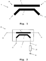
- FIG. 1 an exemplary directional coupler 1 is shown.
- a first strip line 2 has the connections 10, 11.
- a second strip line 3 has the connections 12, 13.
- the two strip lines 2, 3 are arranged in a large spatial proximity on a substrate, not shown here.
- signals couple to terminal 12 with low attenuation, and to terminal 13 with high attenuation.
- Signals applied to terminal 11 couple with less Damping to port 13, and high damping to port 12.
- a signal is applied to terminal 11.
- the signal is applied to the first stripline 2 and couples to the second stripline 3. Since the terminals 12, 13 of the second stripline 3 are not terminated in this example, a significant portion of the signal coupled to the terminal 13 is reflected. This significantly deteriorates the directivity of the directional coupler. By an adapted termination on the terminal 13, this can be avoided to some extent. However, such a conclusion is frequency-selective, which causes a frequency dependence of the directivity.
- Fig. 2 shows an embodiment of the directional coupler according to the invention.
- the directional coupler 30 shown here has the connections 10, 11, 12, 13.
- the directional coupler according to the invention additionally includes a terminating impedance 20 connected to the connection 13.
- the terminating impedance 20 is furthermore connected to a ground connection 21.
- a conventional directional coupler 1 is used within the directional coupler 30 according to the invention. This can be both a stripline directional coupler, as in Fig. 1 represented, as well as any directional coupler be of a different design.
- a pure ohmic resistance is connected as a terminating impedance 20 to the terminal 13.
- the terminal 11 is selectively mismatched by the terminating impedance 20. This results in the reflection of a part of the signal applied to the terminal 13.
- the terminating impedance 20 is selected such that the attenuation of the signal reflected at the terminal 13 corresponds to the attenuation of the signal coupled to the terminal 12. In this example, both attenuations are set to -35dB.
- Phase difference is less than 180 °, so this phase difference must be adjusted by means of the terminating impedance 20.
- the terminating impedance 20 By using inductors, capacitors and ohmic resistors, a phase jump of the reflected signal at the terminal 13 is intentionally caused. However, such an artificially induced phase shift has a certain frequency selectivity. An optimal directivity is thus only in a small frequency range too achieve.
- a terminating impedance is used which is lower than in the case of a matched termination. A phase jump is achieved so reliably.
Landscapes
- Cable Transmission Systems, Equalization Of Radio And Reduction Of Echo (AREA)
- Variable-Direction Aerials And Aerial Arrays (AREA)
- Dc Digital Transmission (AREA)
Description
- Die Erfindung betrifft einen Richtkoppler zur gerichteten Übertragung von Hochfrequenz-Signalen.
- Zum Stand der Technik sei hier z.B. auf die
US 5,424,694 verwiesen. In dieser wird ein Richtkoppler beschrieben, welcher in Streifenleitungstechnik auf einer Substratebene aufgebaut ist. Durch ohmsche Widerstände und Induktivitäten wird das Frequenzverhalten des Richtkopplers beeinflusst. Eine gezielte elektrische Verlängerung der gekoppelten Leitungen wird durchgeführt. Eine Überlagerung von Signalen zur Ausnutzung von Interferenz findet jedoch nicht statt. - Herkömmlich werden in Richtkopplern gekoppelte Leitungen eingesetzt. Mit einem einlagigen Aufbau auf einer Leiterplatte lassen sich jedoch lediglich geringe Richtschärfen erzielen. Herkömmlich werden die Abschlüsse von Richtkopplern möglichst genau an den gewünschten Abschlusswiderstand von typischerweise 50Ω angepasst. Dies geht auch aus der
US 5,424,694 hervor. Dies resultiert in einer für die meisten Anwendungen verwendbaren Richtschärfe. - Eine Richtschärfe von über 30dB lässt sich bei herkömmlichem Aufbau erst mit einem mindestens dreilagigen oder mechanisch sehr komplexen Aufbau oder durch eine explizierte Optimierung der Richtschärfe jedes einzelnen Richtkopplers während der Herstellung erreichen.
- Das Dokument
US 4 644 260 A zeigt einen Richtkoppler, dessen Isolationsanschluss mit einem Abschluss beschaltet ist. - Auch das Dokument
JP 2008 219175 A - Das Dokument WAN-KYU KIM ET AL:"A Passive Circulator with High Isolation using a Directional Coupler for RFID" MICROWAVE SYMPOSIUM DIGEST, 2006. IEEE MTT - S INTERNATIONAL, IEEE, PI, 1. Juni 2006, Seiten 1177 - 1180 zeigt die Erhöhung der Richtschärfe eines Richtkopplers durch gezielte Fehlanpassung des Isolationsanschlusses mittels eines ohmischen Widerstandes und einer Induktivität.
- Das Dokument PENG BAI ET AL: "A Novel RX-TX Front-Ends for Passive RFID Reader with High Isolation", MICROWAVE, ANTENNA, PROPAGATION AMD EMC TECHNOLOGIES FOR WIRELESS COMMUNICATIONS, 2007 INTERNATIONAL SYMPOSIUM ON, IEEE, Pl, 1. August 2007 Seiten 332 - 335, ISBN: 978-1-4244-1044-6 zeigt die gezielte Erhöhung der Richtschärfe eines Richtkopplers durch Fehlanpassung eines Abschlusses des Richtkopplers.
- Die Dokumente
US 2003/011442 und Feng Wei ET AL: "A NEW DIRECTIONAL COUPLER FOR UHF RFID READER",Microwave and Optical Technology Letters, Bd. 50, Nr. 7, 31. Juli 2008 (2008-07-31), Seiten 1973-1975 offenbaren dann weitere Richtkoppler, die eine verbesserte Richtschärfe bedingt durch eine gezielte Fehlanpassung an einem Anschluss bzw. an mehreren Anschlüssen besitzen. - Der Erfindung liegt die Aufgabe zu Grunde, einen Richtkoppler zu schaffen, welcher bei geringem Fertigungsaufwand und geringem Platzbedarf eine hohe Richtgüte erzielt.
- Die Aufgabe wird erfindungsgemäß für die Vorrichtung durch die Merkmale des unabhängigen Anspruchs 1 gelöst. Vorteilhafte Weiterbildungen sind Gegenstand der hierauf rückbezogenen Unteransprüche.
- Ein Richtkoppler verfügt über zumindest vier Anschlüsse, die sich an den Enden von zwei in räumlicher Nähe angeordneten Streifenleitungen befinden, und eine Abschlussimpedanz. Der Richtkoppler ist derart aufgebaut, dass Signale von einem ersten Anschluss an einen dritten Anschluss mit geringer Dämpfung koppeln, und dass Signale von einem zweiten Anschluss an den dritten Anschluss mit sehr hoher Dämpfung koppeln. Weiterhin ist der Richtkoppler derart aufgebaut, dass Signale von dem ersten Anschluss an einen vierten Anschluss mit sehr hoher Dämpfung koppeln, und dass Signale von dem zweiten Anschluss an den vierten Anschluss mit geringer Dämpfung koppeln. Der vierte Anschluss ist dabei mit der Abschlussimpedanz verbunden. Die Abschlussimpedanz ist derart dimensioniert, dass sie eine gezielte Fehlanpassung des vierten Anschlusses und eine Reflexion eines Anteils eines an dem vierten Anschluss eingehenden Signals bewirkt. Das am vierten Anschluss reflektierte Signal und ein am dritten Anschluss anliegendes Signal interferieren dabei zumindest teilweise destruktiv. Die Abschlussimpedanz ist dabei derart dimensioniert, dass sie einen Phasenunterschied des am vierten Anschluss reflektierten Signals gegenüber dem am dritten Anschluss eingehenden Signal von 180° bewirkt. Die Abschlussimpedanz ist dabei ein ohmscher Widerstand und eine Induktivität und eine Kapazität. So ist eine sehr hohe Richtschärfe bei geringer Frequenzselektivität und geringem Herstellungsaufwand gewährleistet. Auch ein geringer Platzbedarf ist die Folge.
- Vorteilhafterweise beinhaltet der Richtkoppler zumindest zwei Streifenleitungen. Eine erste Streifenleitung verbindet bevorzugt den ersten Anschluss mit dem zweiten Anschluss. Eine zweite Streifenleitung verbindet bevorzugt den dritten Anschluss mit dem vierten Anschluss. Die beiden Streifenleitungen sind bevorzugt in räumlicher Nähe zueinander angeordnet. So ist ein Einsatz von verbreiteten Richtkopplern möglich. Streifenleitungsrichtkoppler sind weiterhin sehr einfach herzustellen und verursachen nur einen geringen Platzbedarf.
- Die Abschlussimpedanz ist bevorzugt derart dimensioniert, dass die Amplituden des am vierten Anschluss reflektierten Signals und des am dritten Anschluss eingehenden Signals weitgehend identisch sind.
- Der Richtkoppler ist vorteilhafterweise derart aufgebaut, dass von dem ersten Anschluss oder dem zweiten Anschluss an den dritten Anschluss und an den vierten Anschluss gekoppelte Signale um einen bestimmten Winkel phasenverschoben sind. So kann die Abschlussimpedanz gezielt ausgewählt werden, um den Phasenunterschied des am vierten Anschluss reflektierten Signals gegenüber dem am dritten Anschluss eingehenden Signals auf 180° zu bringen.
- Der Richtkoppler ist bevorzugt derart aufgebaut, dass von dem ersten Anschluss oder dem zweiten Anschluss an den dritten Anschluss und an den vierten Anschluss gekoppelte Signale um 180° phasenverschoben sind. So ist eine Einstellung der Phasenverschiebung durch die Abschlussimpedanz nicht notwendig.
- Nachfolgend wird die Erfindung anhand der Zeichnung, in der ein vorteilhaftes Ausführungsbeispiel der Erfindung dargestellt ist, beispielhaft beschrieben. In der Zeichnung zeigen:
- Fig. 1
- einen beispielhaften Richtkoppler, und
- Fig. 2
- ein Ausführungsbeispiel des erfindungsgemäßen Richtkopplers.
- Zunächst wird anhand der
Fig. 1 ein beispielhafter Richtkoppler und seine Funktionsweise erläutert. MittelsFig. 2 wird anschließend der Aufbau und die Funktionsweise des erfindungsgemäßen Richtkopplers veranschaulicht. - Identische Elemente wurden in ähnlichen Abbildungen zum Teil nicht wiederholt dargestellt und beschrieben.
- In
Fig. 1 wird ein beispielhafter Richtkoppler 1 dargestellt. Eine erste Streifenleitung 2 verfügt über die Anschlüsse 10, 11. Eine zweite Streifenleitung 3 verfügt über die Anschlüsse 12, 13. Die beiden Streifenleitungen 2, 3 sind in großer räumlicher Nähe auf einem hier nicht dargestellten Substrat angeordnet. Am Anschluss 10
angelegte Signale koppeln mit geringer Dämpfung an den Anschluss 12, und mit hoher Dämpfung an den Anschluss 13. Am Anschluss 11 angelegte Signale koppeln mit geringer Dämpfung an den Anschluss 13, und mit hoher Dämpfung an den Anschluss 12. - Beispielsweise wird ein Signal am Anschluss 11 angelegt. Das Signal liegt an der ersten Streifenleitung 2 an und koppelt auf die zweite Streifenleitung 3. Da die Anschlüsse 12, 13 der zweiten Streifenleitung 3 in diesem Beispiel nicht abgeschlossen sind, wird ein nennenswerter Teil des an den Anschluss 13 gekoppelten Signals reflektiert. Dies verschlechtert die Richtschärfe des Richtkopplers deutlich. Durch einen angepassten Abschluss an dem Anschluss 13 kann dies zu einem gewissen Grad vermieden werden. Ein solcher Abschluss ist jedoch frequenzselektiv, was eine Frequenzabhängigkeit der Richtschärfe bewirkt.
-
Fig. 2 zeigt ein Ausführungsbeispiel des erfindungsgemäßen Richtkopplers. Wie auch inFig. 1 verfügt der hier gezeigte Richtkoppler 30 über die Anschlüsse 10, 11, 12, 13. Der erfindungsgemäße Richtkoppler beinhaltet zusätzlich eine am Anschluss 13 angeschlossene Abschlussimpedanz 20. Die Abschlussimpedanz 20 ist weiterhin mit einem Masseanschluss 21 verbunden. Innerhalb des erfindungsgemäßen Richtkopplers 30 wird ein herkömmlicher Richtkoppler 1 eingesetzt. Dieser kann sowohl ein Streifenleitungsrichtkoppler, wie inFig. 1 dargestellt, wie auch ein beliebiger Richtkoppler anderer Bauart sein. - Bei einer Vielzahl von Richtkoppler-Bauarten ergibt sich ein Phasenunterschied der an die beiden Anschlüsse 12, 13 gekoppelten Signale. Dieser beträgt in der Regel 180°. Es sind jedoch auch Richtkoppler bekannt, bei welchen der Phasenunterschied andere Werte annimmt. Auch Richtkoppler ohne den genannten Phasenunterschied sind bekannt.
- Angenommenen der Phasenunterschied beträgt genau 180°, so wird erfindungsgemäß ein rein ohmscher Widerstand als Abschlussimpedanz 20 an den Anschluss 13 angeschlossen.
- Wird beispielsweise ein Signal am Anschluss 11 angelegt, so koppelt es mit geringer Dämpfung, z.B. -20dB an den Anschluss 13 und mit hoher Dämpfung, z.B. -35dB an den Anschluss 12. Bei optimaler Richtschärfe wäre kein Signalanteil am Anschluss 12 messbar. Um diesem Idealzustand möglichst nahe zu kommen, wird der Anschluss 13 durch die Abschlussimpedanz 20 gezielt fehlangepasst. Dies resultiert in der Reflexion eines Teils des am Anschluss 13 anliegenden Signals. Die Abschlussimpedanz 20 wird dabei so gewählt, dass die Dämpfung des am Anschluss 13 reflektierten Signals der Dämpfung des an den Anschluss 12 gekoppelten Signals entspricht. In diesem Beispiel werden beide Dämpfungen auf -35dB eingestellt. Durch den von dem beispielhaften Richtkoppler 1 verursachten Phasenunterschied von 180° tritt destruktive Interferenz auf; die Signale löschen sich aus.
- Angenommenen, der von dem Richtkoppler 1 verursachte. Phasenunterschied beträgt weniger als 180°, so muss dieser Phasenunterschied mittels der Abschlussimpedanz 20 eingestellt werden. Durch Nutzung von Induktivitäten, Kapazitäten und ohmschen Widerständen wird gezielt ein Phasensprung des reflektierten Signals am Anschluss 13 verursacht. Ein solcher künstlich hervorgerufener Phasensprung weist jedoch eine gewisse Frequenzselektivität auf. Eine optimale Richtschärfe ist somit lediglich in einen geringen Frequenzbereich zu erzielen. Bevorzugt wird eine Abschlussimpedanz eingesetzt, welche geringer ist als bei einem angepassten Abschluss. Ein Phasensprung wird so zuverlässig erzielt.
- Die Erfindung ist nicht auf das dargestellte Ausführungsbeispiel beschränkt. Wie bereits erwähnt, können unterschiedliche Richtkoppler-Bauarten eingesetzt werden. Eine erfindungsgemäße Fehlanpassung weiterer Anschlüsse ist vorhanden. Alle vorstehend beschriebenen Merkmale oder in den Figuren gezeigten Merkmale sind im Rahmen der Erfindung beliebig vorteilhaft miteinander kombinierbar.
Claims (5)
- Richtkoppler (30) mit zumindest vier Anschlüssen (10, 11, 12, 13), die sich an den Enden von zwei in räumlicher Nähe angeordneten Streifenleitungen (2,3) befinden, und einer Abschlussimpedanz (20),
wobei der Richtkoppler (30) derart aufgebaut ist, dass Signale von einem ersten Anschluss (10) an einen dritten Anschluss (12) mit geringer Dämpfung koppeln,
wobei Signale von einem zweiten Anschluss (11) an den dritten Anschluss (12) mit hoher Dämpfung koppeln,
wobei Signale von dem ersten Anschluss (10) an einen vierten Anschluss (13) mit hoher Dämpfung koppeln,
wobei Signale von dem zweiten Anschluss (11) an den vierten Anschluss (13) mit geringer Dämpfung koppeln,
wobei der vierte Anschluss (13) mit der Abschlussimpedanz (20) verbunden ist,
wobei die Abschlussimpedanz (20) derart dimensioniert ist, dass sie eine gezielte Fehlanpassung des vierten Anschlusses (13) gegenüber einer der Streifenleitungen (3) und eine Reflexion eines Anteils eines Signals am vierten Anschluss (13) bewirkt,
wobei das am vierten Anschluss (13) reflektierte Signal und ein am dritten Anschluss (12) anliegendes Signal zumindest teilweise auf einer der Streifenleitungen (3) destruktiv interferieren,
wobei die Abschlussimpedanz (20) derart dimensioniert ist, dass sie einen Phasenunterschied des am vierten Anschluss (13) reflektierten Signals gegenüber dem am dritten Anschluss (12) eingehenden Signal von 180° bewirkt,
wobei die Abschlussimpedanz (20) ein ohmscher Widerstand und eine Induktivität und eine Kapazität ist,
wobei der Richtkoppler (30) zumindest eine Fehlanpassung des ersten Anschlusses (10) und/oder des zweiten Anschlusses (11) und/oder des dritten Anschlusses (12) umfasst, und
wobei die zumindest eine Fehlanpassung derart ausgestaltet ist, dass sie zur destruktiven Interferenz der Signale am dritten Anschluss (12) weiter beiträgt. - Richtkoppler nach Anspruch 1,
wobei der Richtkoppler (30) zumindest zwei Streifenleitungen (2, 3) beinhaltet,
wobei eine erste Streifenleitung (2) den ersten Anschluss (10) mit dem zweiten Anschluss (11) verbindet,
wobei eine zweite Streifenleitung (3) den dritten Anschluss (12) mit dem vierten Anschluss (13) verbindet, und
wobei die beiden Steifenleitungen (2, 3) in räumlicher Nähe zueinander angeordnet sind. - Richtkoppler nach einem der Ansprüche 1 oder 2,
wobei die Abschlussimpedanz (20) derart dimensioniert ist, dass die Amplituden des am vierten Anschluss (13) reflektierten Signals und des am dritten Anschluss (12) eingehenden Signals weitgehend identisch sind. - Richtkoppler nach einem der Ansprüche 1 bis 3,
wobei der Richtkoppler (30) derart aufgebaut ist, dass von dem ersten Anschluss (10) oder dem zweiten Anschluss (11) an den dritten Anschluss (12) und an den vierten Anschluss (13) gekoppelte Signale um einen bestimmten Winkel phasenverschoben sind. - Richtkoppler nach einem der Ansprüche 1 bis 4,
wobei der Richtkoppler (30) derart aufgebaut ist, dass von dem ersten Anschluss (10) oder dem zweiten Anschluss (11) an den dritten Anschluss (12) und an den vierten Anschluss (13) gekoppelte Signale um 180° phasenverschoben sind.
Applications Claiming Priority (1)
| Application Number | Priority Date | Filing Date | Title |
|---|---|---|---|
| DE102008051914A DE102008051914A1 (de) | 2008-10-16 | 2008-10-16 | Richtkoppler mit Kompensation der Richtschärfe durch gezielte Fehlanpassung |
Publications (2)
| Publication Number | Publication Date |
|---|---|
| EP2178155A1 EP2178155A1 (de) | 2010-04-21 |
| EP2178155B1 true EP2178155B1 (de) | 2018-10-03 |
Family
ID=41258273
Family Applications (1)
| Application Number | Title | Priority Date | Filing Date |
|---|---|---|---|
| EP09010935.6A Active EP2178155B1 (de) | 2008-10-16 | 2009-08-26 | Richtkoppler mit Kompensation der Richtschärfe durch gezielte Fehlanpassung |
Country Status (3)
| Country | Link |
|---|---|
| EP (1) | EP2178155B1 (de) |
| DE (1) | DE102008051914A1 (de) |
| ES (1) | ES2699631T3 (de) |
Families Citing this family (1)
| Publication number | Priority date | Publication date | Assignee | Title |
|---|---|---|---|---|
| CN105789811A (zh) * | 2016-04-20 | 2016-07-20 | 广东工业大学 | 自补偿定向耦合器 |
Citations (2)
| Publication number | Priority date | Publication date | Assignee | Title |
|---|---|---|---|---|
| US20030011442A1 (en) * | 2001-07-13 | 2003-01-16 | Halappa Ashoka | Microstrip directional coupler loaded by a pair of inductive stubs |
| EP2147478A1 (de) * | 2007-05-11 | 2010-01-27 | Thales | Hyperfrequenzsignalkoppler mit mikrostreifentechnologie |
Family Cites Families (7)
| Publication number | Priority date | Publication date | Assignee | Title |
|---|---|---|---|---|
| US4644260A (en) * | 1985-08-05 | 1987-02-17 | Motorola, Inc. | Coupler with coupled line used to cancel finite directivity |
| US4999593A (en) * | 1989-06-02 | 1991-03-12 | Motorola, Inc. | Capacitively compensated microstrip directional coupler |
| US5424694A (en) | 1994-06-30 | 1995-06-13 | Alliedsignal Inc. | Miniature directional coupler |
| US5625328A (en) * | 1995-09-15 | 1997-04-29 | E-Systems, Inc. | Stripline directional coupler tolerant of substrate variations |
| US20020093384A1 (en) * | 2001-01-12 | 2002-07-18 | Woods Donnie W. | High-directivity and adjusable directional couplers and method therefor |
| DE10121535A1 (de) * | 2001-05-03 | 2002-11-07 | Siemens Ag | Vorrichtung zum Auskoppeln eines vorgegebenen Teils eines hochfrequenten Ausgangssignals |
| JP2008219175A (ja) * | 2007-02-28 | 2008-09-18 | Furuno Electric Co Ltd | 電力合成/分配装置および多点給電円偏波アンテナ |
-
2008
- 2008-10-16 DE DE102008051914A patent/DE102008051914A1/de not_active Withdrawn
-
2009
- 2009-08-26 EP EP09010935.6A patent/EP2178155B1/de active Active
- 2009-08-26 ES ES09010935T patent/ES2699631T3/es active Active
Patent Citations (2)
| Publication number | Priority date | Publication date | Assignee | Title |
|---|---|---|---|---|
| US20030011442A1 (en) * | 2001-07-13 | 2003-01-16 | Halappa Ashoka | Microstrip directional coupler loaded by a pair of inductive stubs |
| EP2147478A1 (de) * | 2007-05-11 | 2010-01-27 | Thales | Hyperfrequenzsignalkoppler mit mikrostreifentechnologie |
Non-Patent Citations (4)
| Title |
|---|
| D B LEESON: "Microwave Filters", EE1194 RF LECTURE NOTES, 21 December 1999 (1999-12-21), XP055401997, Retrieved from the Internet <URL:http://home.sandiego.edu/~ekim/e194rfs01/filterek.pdf> [retrieved on 20170829] * |
| DAVID M POZAR: "The terminated lossless transmission line; Impedance matching and tuning", MICROWAVE ENGINEERING, 31 December 1998 (1998-12-31), US, XP055401994, ISBN: 978-0-471-17096-9, Retrieved from the Internet <URL:Microwave Engineering 2nd Edition> [retrieved on 20170829] * |
| FENG WEI ET AL: "A NEW DIRECTIONAL COUPLER FOR UHF RFID READER", MICROWAVE AND OPTICAL TECHNOLOGY LETTERS, vol. 50, no. 7, 31 July 2008 (2008-07-31), pages 1973 - 1975, XP055336194, DOI: 10.1002/mop * |
| PENG BAI ET AL: "A Novel RX-TX Front-Ends for Passive RFID Reader with High Isolation", MICROWAVE, ANTENNA, PROPAGATION AND EMC TECHNOLOGIES FOR WIRELESS COMM UNICATIONS, 2007 INTERNATIONAL SYMPOSIUM ON, IEEE, PI, 1 August 2007 (2007-08-01), pages 332 - 335, XP031167703, ISBN: 978-1-4244-1044-6 * |
Also Published As
| Publication number | Publication date |
|---|---|
| ES2699631T3 (es) | 2019-02-12 |
| DE102008051914A1 (de) | 2010-04-22 |
| EP2178155A1 (de) | 2010-04-21 |
Similar Documents
| Publication | Publication Date | Title |
|---|---|---|
| DE102015115566B4 (de) | System und Verfahren für einen Richtkoppler | |
| DE102015115332B4 (de) | System und Verfahren für ein Richtkopplermodul | |
| DE102010024439B4 (de) | Antennenvorrichtung | |
| DE102014114200A1 (de) | System und Verfahren für einen Hochfrequenzkoppler | |
| DE102010040290A1 (de) | Richtkoppler | |
| DE60005656T2 (de) | Transformator mit ubermittlungsleitung für impedanzanpassung | |
| DE202020106896U1 (de) | Hochfrequenzmodul und Kommunikationsgerät | |
| DE112013004185B4 (de) | Richtkoppler | |
| DE10202699B4 (de) | Nichtreziprokes Schaltungsbauelement und Kommunikationsvorrichtung, die dasselbe enthält | |
| DE102019204163B3 (de) | Erzeugung eines Abstimmsignals zur Abstimmung einer magnetischen Antenne | |
| EP2178155B1 (de) | Richtkoppler mit Kompensation der Richtschärfe durch gezielte Fehlanpassung | |
| WO2012084379A1 (de) | Richtkoppler | |
| DE102011004042B4 (de) | Energieleitungskommunikationssystem | |
| EP3462612B1 (de) | Antennenschaltung für nahfeld-antennen | |
| DE102014203228B4 (de) | Richtkoppler und Magnetresonanztomographieeinrichtung | |
| DE102010048619A1 (de) | Antennenanordnung | |
| DE102012112571B3 (de) | Schaltungsanordnung | |
| DE10217387B4 (de) | Elektrisches Anpassungsnetzwerk mit einer Transformationsleitung | |
| DE69716146T2 (de) | Hochfrequenz-Leistungsmesseinrichtung | |
| EP2160793B1 (de) | Richtkoppler mit induktiv kompensierter richtschärfe | |
| DE10348722B4 (de) | Elektrisches Anpassungsnetzwerk mit einer Transformationsleitung | |
| DE3644476C2 (de) | Verfahren zur Impedanztransformation | |
| EP2192009B1 (de) | Identifikationsgeber für ein elektronisches Zugangssystem und eine elektronische Wegfahrsperre | |
| DE102010046746B4 (de) | Elektrisches Dämpfungsglied | |
| WO2011104156A1 (de) | Breitbandig betreibbare impedanzanpassschaltung |
Legal Events
| Date | Code | Title | Description |
|---|---|---|---|
| PUAI | Public reference made under article 153(3) epc to a published international application that has entered the european phase |
Free format text: ORIGINAL CODE: 0009012 |
|
| 17P | Request for examination filed |
Effective date: 20091218 |
|
| AK | Designated contracting states |
Kind code of ref document: A1 Designated state(s): AT BE BG CH CY CZ DE DK EE ES FI FR GB GR HR HU IE IS IT LI LT LU LV MC MK MT NL NO PL PT RO SE SI SK SM TR |
|
| AX | Request for extension of the european patent |
Extension state: AL BA RS |
|
| STAA | Information on the status of an ep patent application or granted ep patent |
Free format text: STATUS: EXAMINATION IS IN PROGRESS |
|
| GRAP | Despatch of communication of intention to grant a patent |
Free format text: ORIGINAL CODE: EPIDOSNIGR1 |
|
| STAA | Information on the status of an ep patent application or granted ep patent |
Free format text: STATUS: GRANT OF PATENT IS INTENDED |
|
| INTG | Intention to grant announced |
Effective date: 20180412 |
|
| GRAS | Grant fee paid |
Free format text: ORIGINAL CODE: EPIDOSNIGR3 |
|
| GRAA | (expected) grant |
Free format text: ORIGINAL CODE: 0009210 |
|
| STAA | Information on the status of an ep patent application or granted ep patent |
Free format text: STATUS: THE PATENT HAS BEEN GRANTED |
|
| AK | Designated contracting states |
Kind code of ref document: B1 Designated state(s): AT BE BG CH CY CZ DE DK EE ES FI FR GB GR HR HU IE IS IT LI LT LU LV MC MK MT NL NO PL PT RO SE SI SK SM TR |
|
| REG | Reference to a national code |
Ref country code: GB Ref legal event code: FG4D Free format text: NOT ENGLISH |
|
| REG | Reference to a national code |
Ref country code: CH Ref legal event code: EP Ref country code: AT Ref legal event code: REF Ref document number: 1049634 Country of ref document: AT Kind code of ref document: T Effective date: 20181015 |
|
| REG | Reference to a national code |
Ref country code: IE Ref legal event code: FG4D Free format text: LANGUAGE OF EP DOCUMENT: GERMAN Ref country code: DE Ref legal event code: R096 Ref document number: 502009015330 Country of ref document: DE |
|
| REG | Reference to a national code |
Ref country code: NL Ref legal event code: MP Effective date: 20181003 |
|
| REG | Reference to a national code |
Ref country code: ES Ref legal event code: FG2A Ref document number: 2699631 Country of ref document: ES Kind code of ref document: T3 Effective date: 20190212 |
|
| REG | Reference to a national code |
Ref country code: LT Ref legal event code: MG4D |
|
| PG25 | Lapsed in a contracting state [announced via postgrant information from national office to epo] |
Ref country code: NL Free format text: LAPSE BECAUSE OF FAILURE TO SUBMIT A TRANSLATION OF THE DESCRIPTION OR TO PAY THE FEE WITHIN THE PRESCRIBED TIME-LIMIT Effective date: 20181003 |
|
| PG25 | Lapsed in a contracting state [announced via postgrant information from national office to epo] |
Ref country code: CZ Free format text: LAPSE BECAUSE OF FAILURE TO SUBMIT A TRANSLATION OF THE DESCRIPTION OR TO PAY THE FEE WITHIN THE PRESCRIBED TIME-LIMIT Effective date: 20181003 Ref country code: IS Free format text: LAPSE BECAUSE OF FAILURE TO SUBMIT A TRANSLATION OF THE DESCRIPTION OR TO PAY THE FEE WITHIN THE PRESCRIBED TIME-LIMIT Effective date: 20190203 Ref country code: NO Free format text: LAPSE BECAUSE OF FAILURE TO SUBMIT A TRANSLATION OF THE DESCRIPTION OR TO PAY THE FEE WITHIN THE PRESCRIBED TIME-LIMIT Effective date: 20190103 Ref country code: BG Free format text: LAPSE BECAUSE OF FAILURE TO SUBMIT A TRANSLATION OF THE DESCRIPTION OR TO PAY THE FEE WITHIN THE PRESCRIBED TIME-LIMIT Effective date: 20190103 Ref country code: PL Free format text: LAPSE BECAUSE OF FAILURE TO SUBMIT A TRANSLATION OF THE DESCRIPTION OR TO PAY THE FEE WITHIN THE PRESCRIBED TIME-LIMIT Effective date: 20181003 Ref country code: FI Free format text: LAPSE BECAUSE OF FAILURE TO SUBMIT A TRANSLATION OF THE DESCRIPTION OR TO PAY THE FEE WITHIN THE PRESCRIBED TIME-LIMIT Effective date: 20181003 Ref country code: LT Free format text: LAPSE BECAUSE OF FAILURE TO SUBMIT A TRANSLATION OF THE DESCRIPTION OR TO PAY THE FEE WITHIN THE PRESCRIBED TIME-LIMIT Effective date: 20181003 Ref country code: LV Free format text: LAPSE BECAUSE OF FAILURE TO SUBMIT A TRANSLATION OF THE DESCRIPTION OR TO PAY THE FEE WITHIN THE PRESCRIBED TIME-LIMIT Effective date: 20181003 Ref country code: HR Free format text: LAPSE BECAUSE OF FAILURE TO SUBMIT A TRANSLATION OF THE DESCRIPTION OR TO PAY THE FEE WITHIN THE PRESCRIBED TIME-LIMIT Effective date: 20181003 |
|
| PG25 | Lapsed in a contracting state [announced via postgrant information from national office to epo] |
Ref country code: SE Free format text: LAPSE BECAUSE OF FAILURE TO SUBMIT A TRANSLATION OF THE DESCRIPTION OR TO PAY THE FEE WITHIN THE PRESCRIBED TIME-LIMIT Effective date: 20181003 Ref country code: GR Free format text: LAPSE BECAUSE OF FAILURE TO SUBMIT A TRANSLATION OF THE DESCRIPTION OR TO PAY THE FEE WITHIN THE PRESCRIBED TIME-LIMIT Effective date: 20190104 Ref country code: PT Free format text: LAPSE BECAUSE OF FAILURE TO SUBMIT A TRANSLATION OF THE DESCRIPTION OR TO PAY THE FEE WITHIN THE PRESCRIBED TIME-LIMIT Effective date: 20190203 |
|
| REG | Reference to a national code |
Ref country code: DE Ref legal event code: R097 Ref document number: 502009015330 Country of ref document: DE |
|
| PG25 | Lapsed in a contracting state [announced via postgrant information from national office to epo] |
Ref country code: DK Free format text: LAPSE BECAUSE OF FAILURE TO SUBMIT A TRANSLATION OF THE DESCRIPTION OR TO PAY THE FEE WITHIN THE PRESCRIBED TIME-LIMIT Effective date: 20181003 |
|
| PLBE | No opposition filed within time limit |
Free format text: ORIGINAL CODE: 0009261 |
|
| STAA | Information on the status of an ep patent application or granted ep patent |
Free format text: STATUS: NO OPPOSITION FILED WITHIN TIME LIMIT |
|
| PG25 | Lapsed in a contracting state [announced via postgrant information from national office to epo] |
Ref country code: SM Free format text: LAPSE BECAUSE OF FAILURE TO SUBMIT A TRANSLATION OF THE DESCRIPTION OR TO PAY THE FEE WITHIN THE PRESCRIBED TIME-LIMIT Effective date: 20181003 Ref country code: EE Free format text: LAPSE BECAUSE OF FAILURE TO SUBMIT A TRANSLATION OF THE DESCRIPTION OR TO PAY THE FEE WITHIN THE PRESCRIBED TIME-LIMIT Effective date: 20181003 Ref country code: RO Free format text: LAPSE BECAUSE OF FAILURE TO SUBMIT A TRANSLATION OF THE DESCRIPTION OR TO PAY THE FEE WITHIN THE PRESCRIBED TIME-LIMIT Effective date: 20181003 Ref country code: SK Free format text: LAPSE BECAUSE OF FAILURE TO SUBMIT A TRANSLATION OF THE DESCRIPTION OR TO PAY THE FEE WITHIN THE PRESCRIBED TIME-LIMIT Effective date: 20181003 |
|
| 26N | No opposition filed |
Effective date: 20190704 |
|
| PG25 | Lapsed in a contracting state [announced via postgrant information from national office to epo] |
Ref country code: SI Free format text: LAPSE BECAUSE OF FAILURE TO SUBMIT A TRANSLATION OF THE DESCRIPTION OR TO PAY THE FEE WITHIN THE PRESCRIBED TIME-LIMIT Effective date: 20181003 |
|
| PG25 | Lapsed in a contracting state [announced via postgrant information from national office to epo] |
Ref country code: TR Free format text: LAPSE BECAUSE OF FAILURE TO SUBMIT A TRANSLATION OF THE DESCRIPTION OR TO PAY THE FEE WITHIN THE PRESCRIBED TIME-LIMIT Effective date: 20181003 |
|
| PG25 | Lapsed in a contracting state [announced via postgrant information from national office to epo] |
Ref country code: LI Free format text: LAPSE BECAUSE OF NON-PAYMENT OF DUE FEES Effective date: 20190831 Ref country code: CH Free format text: LAPSE BECAUSE OF NON-PAYMENT OF DUE FEES Effective date: 20190831 Ref country code: MC Free format text: LAPSE BECAUSE OF FAILURE TO SUBMIT A TRANSLATION OF THE DESCRIPTION OR TO PAY THE FEE WITHIN THE PRESCRIBED TIME-LIMIT Effective date: 20181003 Ref country code: LU Free format text: LAPSE BECAUSE OF NON-PAYMENT OF DUE FEES Effective date: 20190826 |
|
| REG | Reference to a national code |
Ref country code: BE Ref legal event code: MM Effective date: 20190831 |
|
| PG25 | Lapsed in a contracting state [announced via postgrant information from national office to epo] |
Ref country code: IE Free format text: LAPSE BECAUSE OF NON-PAYMENT OF DUE FEES Effective date: 20190826 |
|
| PG25 | Lapsed in a contracting state [announced via postgrant information from national office to epo] |
Ref country code: BE Free format text: LAPSE BECAUSE OF NON-PAYMENT OF DUE FEES Effective date: 20190831 Ref country code: IT Free format text: LAPSE BECAUSE OF NON-PAYMENT OF DUE FEES Effective date: 20190826 |
|
| REG | Reference to a national code |
Ref country code: AT Ref legal event code: MM01 Ref document number: 1049634 Country of ref document: AT Kind code of ref document: T Effective date: 20190826 |
|
| PG25 | Lapsed in a contracting state [announced via postgrant information from national office to epo] |
Ref country code: AT Free format text: LAPSE BECAUSE OF NON-PAYMENT OF DUE FEES Effective date: 20190826 |
|
| REG | Reference to a national code |
Ref country code: ES Ref legal event code: FD2A Effective date: 20210107 |
|
| PG25 | Lapsed in a contracting state [announced via postgrant information from national office to epo] |
Ref country code: ES Free format text: LAPSE BECAUSE OF NON-PAYMENT OF DUE FEES Effective date: 20190827 |
|
| PG25 | Lapsed in a contracting state [announced via postgrant information from national office to epo] |
Ref country code: CY Free format text: LAPSE BECAUSE OF FAILURE TO SUBMIT A TRANSLATION OF THE DESCRIPTION OR TO PAY THE FEE WITHIN THE PRESCRIBED TIME-LIMIT Effective date: 20181003 |
|
| PG25 | Lapsed in a contracting state [announced via postgrant information from national office to epo] |
Ref country code: MT Free format text: LAPSE BECAUSE OF FAILURE TO SUBMIT A TRANSLATION OF THE DESCRIPTION OR TO PAY THE FEE WITHIN THE PRESCRIBED TIME-LIMIT Effective date: 20181003 Ref country code: HU Free format text: LAPSE BECAUSE OF FAILURE TO SUBMIT A TRANSLATION OF THE DESCRIPTION OR TO PAY THE FEE WITHIN THE PRESCRIBED TIME-LIMIT; INVALID AB INITIO Effective date: 20090826 |
|
| PG25 | Lapsed in a contracting state [announced via postgrant information from national office to epo] |
Ref country code: MK Free format text: LAPSE BECAUSE OF FAILURE TO SUBMIT A TRANSLATION OF THE DESCRIPTION OR TO PAY THE FEE WITHIN THE PRESCRIBED TIME-LIMIT Effective date: 20181003 |
|
| P01 | Opt-out of the competence of the unified patent court (upc) registered |
Effective date: 20230525 |
|
| PGFP | Annual fee paid to national office [announced via postgrant information from national office to epo] |
Ref country code: DE Payment date: 20250819 Year of fee payment: 17 |
|
| PGFP | Annual fee paid to national office [announced via postgrant information from national office to epo] |
Ref country code: GB Payment date: 20250822 Year of fee payment: 17 |
|
| PGFP | Annual fee paid to national office [announced via postgrant information from national office to epo] |
Ref country code: FR Payment date: 20250821 Year of fee payment: 17 |