EP2183768B1 - Implantation d'ions à haute température de transistors à électrons à grande mobilité à base de nitrure - Google Patents
Implantation d'ions à haute température de transistors à électrons à grande mobilité à base de nitrure Download PDFInfo
- Publication number
- EP2183768B1 EP2183768B1 EP08795949.0A EP08795949A EP2183768B1 EP 2183768 B1 EP2183768 B1 EP 2183768B1 EP 08795949 A EP08795949 A EP 08795949A EP 2183768 B1 EP2183768 B1 EP 2183768B1
- Authority
- EP
- European Patent Office
- Prior art keywords
- layer
- implanted
- forming
- implantation
- implanting
- Prior art date
- Legal status (The legal status is an assumption and is not a legal conclusion. Google has not performed a legal analysis and makes no representation as to the accuracy of the status listed.)
- Active
Links
Images

Classifications
-
- H—ELECTRICITY
- H10—SEMICONDUCTOR DEVICES; ELECTRIC SOLID-STATE DEVICES NOT OTHERWISE PROVIDED FOR
- H10P—GENERIC PROCESSES OR APPARATUS FOR THE MANUFACTURE OR TREATMENT OF DEVICES COVERED BY CLASS H10
- H10P30/00—Ion implantation into wafers, substrates or parts of devices
- H10P30/20—Ion implantation into wafers, substrates or parts of devices into semiconductor materials, e.g. for doping
- H10P30/21—Ion implantation into wafers, substrates or parts of devices into semiconductor materials, e.g. for doping of electrically active species
-
- H—ELECTRICITY
- H10—SEMICONDUCTOR DEVICES; ELECTRIC SOLID-STATE DEVICES NOT OTHERWISE PROVIDED FOR
- H10D—INORGANIC ELECTRIC SEMICONDUCTOR DEVICES
- H10D30/00—Field-effect transistors [FET]
- H10D30/01—Manufacture or treatment
- H10D30/015—Manufacture or treatment of FETs having heterojunction interface channels or heterojunction gate electrodes, e.g. HEMT
-
- H—ELECTRICITY
- H10—SEMICONDUCTOR DEVICES; ELECTRIC SOLID-STATE DEVICES NOT OTHERWISE PROVIDED FOR
- H10D—INORGANIC ELECTRIC SEMICONDUCTOR DEVICES
- H10D62/00—Semiconductor bodies, or regions thereof, of devices having potential barriers
- H10D62/80—Semiconductor bodies, or regions thereof, of devices having potential barriers characterised by the materials
- H10D62/85—Semiconductor bodies, or regions thereof, of devices having potential barriers characterised by the materials being Group III-V materials, e.g. GaAs
-
- H—ELECTRICITY
- H10—SEMICONDUCTOR DEVICES; ELECTRIC SOLID-STATE DEVICES NOT OTHERWISE PROVIDED FOR
- H10D—INORGANIC ELECTRIC SEMICONDUCTOR DEVICES
- H10D64/00—Electrodes of devices having potential barriers
- H10D64/60—Electrodes characterised by their materials
- H10D64/62—Electrodes ohmically coupled to a semiconductor
-
- H—ELECTRICITY
- H10—SEMICONDUCTOR DEVICES; ELECTRIC SOLID-STATE DEVICES NOT OTHERWISE PROVIDED FOR
- H10P—GENERIC PROCESSES OR APPARATUS FOR THE MANUFACTURE OR TREATMENT OF DEVICES COVERED BY CLASS H10
- H10P30/00—Ion implantation into wafers, substrates or parts of devices
- H10P30/20—Ion implantation into wafers, substrates or parts of devices into semiconductor materials, e.g. for doping
- H10P30/202—Ion implantation into wafers, substrates or parts of devices into semiconductor materials, e.g. for doping characterised by the semiconductor materials
- H10P30/206—Ion implantation into wafers, substrates or parts of devices into semiconductor materials, e.g. for doping characterised by the semiconductor materials into Group III-V semiconductors
-
- H—ELECTRICITY
- H10—SEMICONDUCTOR DEVICES; ELECTRIC SOLID-STATE DEVICES NOT OTHERWISE PROVIDED FOR
- H10D—INORGANIC ELECTRIC SEMICONDUCTOR DEVICES
- H10D62/00—Semiconductor bodies, or regions thereof, of devices having potential barriers
- H10D62/80—Semiconductor bodies, or regions thereof, of devices having potential barriers characterised by the materials
- H10D62/85—Semiconductor bodies, or regions thereof, of devices having potential barriers characterised by the materials being Group III-V materials, e.g. GaAs
- H10D62/8503—Nitride Group III-V materials, e.g. AlN or GaN
Definitions
- the present invention relates to semiconductor devices and, more particularly, to Group-III nitride based high electron mobility transistors (HEMTs).
- HEMTs Group-III nitride based high electron mobility transistors
- HEMTs are semiconductor devices that can be used for a variety of applications including microwave and millimeter-wave communications, radar, radio astronomy, cell phones, direct broadcast satellite receivers, and electronic warfare systems.
- HEMTs are field effect transistors that utilize the heterojunction between two materials having different bandgaps to form a conductive channel rather than a doped region. HEMTs typically do not require impurities to form the conductive layer and therefore allow for higher electron mobility.
- HEMTs are regularly fabricated from semiconductor materials such as silicon (Si) and gallium arsenide (GaAs).
- Si has a low electron mobility, which generates a high source resistance; therefore, Si semiconductor materials may not be well suited for high power, high frequency, and high temperature applications.
- GaAs semiconductor materials have higher electron mobility and a lower source resistance than Si, which allows them to operate at higher frequencies.
- GaAs has, however, a relatively small bandgap preventing the use of GaAs HEMTs in high power at high frequency applications.
- GaN gallium nitride
- AlGaN aluminum nitride and gallium nitride
- the use of AlGaN layered upon GaN and the mismatch of the crystal structures of the two materials and their different bandgap energies results in the creation of a two-dimensional electron gas (2DEG) under certain circumstances.
- the 2DEG layer accumulates in the smaller bandgap material and contains a very high electron concentration. Electrons originating in the wider-bandgap material transfer to the 2DEG allowing for a higher electron mobility.
- AlGaN/GaN HEMTs greater performance than metal-semiconductor field effect transistors (MESFETs) for highfrequency applications.
- MESFETs metal-semiconductor field effect transistors
- One method of fabricating an AlGaN/GaNHEMT includes forming a layer of GaN on a substrate (typically silicon carbide (SiC)), forming a thin layer of AlGaN on the GaN layer, and providing ohmic contacts and a gate contact on the AlGaN layer.
- a substrate typically silicon carbide (SiC)
- SiC silicon carbide
- Another method of forming low-resistive ohmic contacts on AlGaN/GaNHEMTs generally well-understood within the art employs ion implantation at the ohmic contact region. Implantation in this manner allows the use of a Ti/Ni/Al contact, thus eliminating the poor morphology created by the use of Au.
- this implantation process creates another problem because of the high doses of implantation ions that must be used in order to get sufficient activation rates within the implanted regions.
- the high doses of implantation ions create large amounts of crystal destruction. This destruction can be corrected by annealing the device; however, SiC and AlGaN are difficult to recrystallize by annealing. In order to recrystallize SiC and AlGaN properly, longer annealing times can be used. Longer anneal times, however, damage other features of the device.
- the invention is a method of forming a high electron mobility transistor.
- the method includes implanting a Group III nitride layer at a defined position with ions that when implanted produce an improved ohmic contact between the layer and contact metals.
- Implantation is carried out at a temperature between 250°C and 900°C .
- An ohmic contact is added to the implanted defined position on the Group III nitride layer.
- the method includes carrying out the implantation with an ion beam current high enough to successfully implant ions within the Group III nitride layer, but below a current that would melt or destroy the Group III nitride layer and at a temperature between 205°C and 900° C
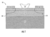
- Figure 1 is a schematic cross-sectional view of an AlGaN/GaN HEMT made according to an embodiment of the present invention.
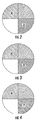
- Figures 2-4 are photographs of three gallium nitride wafers implanted with silicon ions under different conditions.
- Figure 5 depicts the transmission spectrums in the visible range of wafers implanted with silicon ions under various conditions.
- FIG. 1 illustrates a schematic cross-section of an AlGaN/GaN based HEMT 10 constructed in accordance with an embodiment of the present invention.
- the HEMT includes a substrate 11 formed from materials generally well-understood within the art (e.g., silicon carbide (SiC) or sapphire (Al 2 O 3 )).
- a GaN layer 12 is provided on the substrate 11.
- the HEMT 10 includes an AlGaN layer 13 provided on top of the GaN layer 12.
- SiC forms the substrate 11.
- the crystal lattice structure of SiC matches more closely to the Group-III nitrides than sapphire, resulting in higher quality Group-III nitride films.
- SiC has a very high thermal conductivity which allows for higher total output power of the device.
- the AlGaN layer 13 has a wider bandgap than the GaN layer 12 which results in a free charge transfer from the AlGaN layer 13 to the GaN layer 12.
- Charge accumulates at the interface of the AlGaN layer 13 and the GaN layer 12 forming a two-dimensional electron gas (2DEG) (not shown).
- the 2DEG has very high electron mobility resulting in a HEMT 10 with very high transconductance at high frequencies.
- the voltage applied to the gate 14 controls the electron flow in the 2DEG under the gate 14, allowing for control over the total electron flow.
- the gate 14 is a Schottky gate.
- the source contact 15 and drain contact 16 provided on the AlGaN layer 13 are preferably formed of alloys of titanium (Ti), aluminum (Al), and nickel (Ni).
- Traditional alloys used for ohmic contacts 15 and 16 are formed of Ti, Al, Ni as well as gold (Au).
- Au gold
- the addition of Au gives the alloy poor morphology, so the contacts 15 and 16 of the present invention preferably do not include Au.
- Other candidate compositions for the ohmic contact include titanium-tungsten-nitride (Ti-W-N), titanium-nitride (Ti-N), molybdenum (Mo) and molybdenum silicides.
- High temperature ion implantation using a high ion beam current of an n-type dopant creates the implanted regions 20 and 21.
- the dopant ions are Si + .
- These implanted regions 20 and 21 allow the contacts 15 and 16 to be ohmic towards the 2DEG.
- High temperature should be understood to include temperatures that are below a temperature at which surface problems causing leakage at the gate 14 or epitaxial layer dissociation would occur but higher than room temperature.
- the temperature at which implantation occurs is between 250° C and 900° C.
- High ion beam current as used herein should be understood to include a beam current below that which would melt or destroy the crystal, but high enough to successfully implant ions within the AlGaN and GaN layers 13 and 12.
- the beam current is between 30 ⁇ A and 130 ⁇ A.
- the present invention is an AlGaN/GaNHEMT wherein implanted regions 20 and 21 have been implanted at a temperature of 650° C using an ion beam current of 40 ⁇ A.
- the present invention is an AlGaN/GaNHEMT wherein implanted regions 20 and 21 have been implanted at a temperature of 650° C using an ion beam current of 120 ⁇ A.
- the present invention is an AlGaN/GaN HEMT wherein implanted regions 20 and 21 have been implanted at a temperature of 350° C using an ion beam current of 40 ⁇ A.
- the present invention is an AlGaN/GaN HEMT wherein implanted regions 20 and 21 have been implanted at a temperature of 350° C using an ion beam current of 120 ⁇ A.
- the present invention also includes methods for fabricating HEMTs using high temperature ion implantation.
- U.S. Pat. No. 7,230,284 discloses a method for forming the GaN layer 12 on the substrate 11 and forming the AlGaN layer 13 on the GaN layer 12.
- a mask layer protects only the portion of the AlGaN layer that will not be implanted leaving the crystal exposed in the regions to be implanted.
- the mask layer is a material capable of withstanding the conditions of the high temperature, high ion beam current implantation without otherwise adversely affecting either the implantation step or the device.
- the mask layer may be formed of an oxide.
- the device is then maintained at a high temperature and a high current beam implants n-type dopant ions (e.g. Si + ions) through the AlGaN layer 13 into the GaN layer 12 to form implanted regions 20 and 21.
- n-type dopant ions e.g. Si + ions
- the ions are implanted to a depth that allows the ohmic contacts 15 and 16 to act ohmic towards the 2DEG.
- a protective layer may be placed over the regions to be implanted.
- silicon nitride Si 3 N 4 is the protective layer.
- the protective layer reduces the amount of damage to the AlGaN layer created by the ion beam.
- the use of a protective layer is preferred because AlGaN can be particularly difficult to recrystallize using annealing methods.
- an annealing process improves the damaged implanted regions 20 and 21. Shorter anneal times are desired because the anneal has the potential to damage other parts of the device. Implantation at high temperature results in less damage to the implanted regions and therefore allows shorter anneal times, which reduces the possibility for anneal-based secondary damage.
- Ohmic contacts 15 and 16 are then formed on the AlGaN layer 13 over the implanted regions 20 and 21.
- the ohmic contacts 15 and 16 connect with the 2DEG electronically through the implanted regions 20 and 21.
- an alloy of Ti, Ni, and Al forms the ohmic contacts 15 and 16.
- a gate 14 can be formed on the AlGaN layer 13 over the 2DEG.
- the voltage applied to the gate 14 controls the electron flow in the 2DEG, allowing for control over the total electron flow.
- the gate 14 is a Schottky gate.
- FIGS. 2-4 Each wafer in FIGS. 2-4 is GaN that has been implanted with Si + ions.
- FIGS. 2-4 illustrate that conducting the implantation step of this method at high temperature avoids damaging the implanted crystals as much as implantation at room temperature.
- the lighter shades indicate more light passage based upon less crystal damage, while darker shades indicate less light passage resulting from more crystal damage.
- the top left quarter of the wafer 30 has been implanted using an ion beam current of 120 ⁇ A at a temperature of 350° C.
- the bottom right quarter of the wafer 31 has been implanted using an ion beam current of 120 ⁇ A at room temperature.
- the top left quarter 30 is significantly lighter than the bottom right quarter 31, indicating significantly less damage because of the higher temperature during implantation.
- the top left quarter of the wafer 32 has been implanted using an ion beam current of 120 ⁇ A at a temperature of 650° C.
- the bottom right quarter of the wafer 33 has been implanted using an ion beam current of 120 ⁇ A at room temperature.
- the top left quarter 32 is significantly lighter than the bottom right quarter 33, indicating significantly less damage because of the higher temperature during implantation.
- a comparison of the top left quarter of the wafer 30 in FIG. 2 and the top left quarter of the wafer 32 in FIG. 3 also indicates that implantation at higher temperatures decreases the amount of crystal damage created by the implantation process.
- a high current ion beam provides two distinct advantages over a lower current ion beam. Using a high current ion beam reduces the time it takes to implant a given dose of dopant ions therefore reducing costs. Additionally, the use of a high current ion beam further increases the temperature of the wafer during implantation, resulting in less damage to the implanted crystal.
- the wafer in FIG. 4 illustrates the second advantage of using a higher current ion beam.
- the top left quarter of the wafer 34 has been implanted using an ion beam current of 120 ⁇ A at a temperature of 350° C.
- the bottom right quarter of the wafer 35 has been implanted using an ion beam current of 40 ⁇ A at a temperature of 350° C.
- the top left quarter 34 is significantly lighter than the bottom right quarter 35, indicating significantly less damage because of the higher ion beam current during implantation.
- Some of the reduced damage in the top left quarter 34 may be attributable to the fact that it was effectively annealed at 350° C while the bottom right quarter of the wafer 35 was being implanted.
- the difference in clarity created by the anneal is believed to be less significant than the difference in clarity created by the higher ion beam current.
- FIG. 5 illustrates the previously mentioned lightness and darkness comparisons in a more concrete manner.
- the graph plots the percentage of light transmitted through GaN wafers that have been implanted with Si + versus the wavelength of the light for the visible range.
- the two highest plots one formed of squares and the other of diamonds, indicate the transmission percentages of two GaN wafers that have not been implanted. As shown in FIG. 5 , these unimplanted wafers transmit the highest percentage of visible light.
- the lowest plot, formed of downward pointing triangles indicates the transmission percentage of a GaN wafer implanted with Si + at room temperature with an ion beam current of 120 ⁇ A over the visible range. As shown in FIG. 5 , this wafer transmits the lowest percentage of visible light.
- the mid-level plot formed of circles indicates the transmission percentage of a GaN wafer implanted with Si + at a temperature of 650° C with an ion beam current of 120 ⁇ A over the visible range.
- the mid-level plot formed of diamonds indicates the transmission percentage of a GaN wafer implanted with Si + at a temperature of 350° C with an ion beam current of 120 ⁇ A over the visible range.
- the mid-level plot formed of downward pointing triangles indicates the transmission percentage of a GaN wafer implanted with Si + at a temperature of 350° C with an ion beam current of 40 ⁇ A over the visible range.
- These three mid-levcl plots indicate the transmission spectrums of three different wafers that are embodiments of the present invention. As shown in FIG. 5 , these three wafers transmit more light over the visible range than the wafer implanted at room temperature. FIG. 5 also indicates that these three wafers transmit less light over the visible range than the unimplanted wafers.
- the mid-level plot formed of diamonds i.e ., the wafer implanted at 350° C with a current of 120 ⁇ A
- the mid-level plot formed of downward pointing triangles i.e , the wafer implanted at 350° C with a current of 40 pA. This comparison indicates that wafers implanted at higher beam currents typically transmit a greater percentage of light than wafers implanted at lower beam currents.
- the plots show that implantation at high temperatures (e.g ., the three mid-level plots) produces a wafer that transmits a much higher percentage of visible light than implantation at room temperature ( e.g. , the lowest plot).
- the transmission percentage correlates with less damage to the crystal structure of the wafer. Therefore, implantation at high temperatures creates less damage to the crystal structure of the wafer than implantation at room temperature.
- the plot also shows that a wafer implanted using a higher ion beam current (e.g ., the mid-level plot formed of diamonds) transmits a higher percentage of visible light than a wafer implanted using a lower ion beam current (e.g ., the mid-level plot formed of downward pointing triangles).
- a higher ion beam current e.g ., the mid-level plot formed of diamonds
- a lower ion beam current e.g ., the mid-level plot formed of downward pointing triangles.
- the method of the present invention produces HEMTs with significantly less damage to the crystal than previously disclosed methods. As a result, HEMTs produced using the method of the present invention perform superiorly to prior HEMTs.
- the following table contains data on the performance of a HEMT device implanted at room temperature and a HEMT device implanted at high temperature in accordance with the present invention:
- Implant Temperature RF Power GHz
- Gate-Source Voltage Drain-Source Voltage Current mA/mm
- Gain Output Power Added Efficiency Average On-Resistance Drain Source Current 350° C 10 -2.8 48 43.0 13.7 9.13 51.6 3.54 1007.8 Room Temperature 10 -2.8 48 43.0 11.7 8.42 48.4 3.90 936.4
- the wafers of the table received the same implant dose of 1.00 ⁇ 10 16 atoms/cm 2 of Si + and the same temperature anneal (1080° C).
- the data shows that both wafers were supplied with the same RF power, gate-source voltage, drain-source voltage, and current.
- the high temperature implanted HEMT had a higher gain, output power, power added efficiency and drain source current as well as a lower average on-resistance. This data indicates that devices formed according to the present invention have better device performance than devices formed using ion implantation at room temperature.
Landscapes
- Junction Field-Effect Transistors (AREA)
- Electrodes Of Semiconductors (AREA)
Claims (12)
- Procédé de formation d'un transistor à haute mobilité électronique (10) comprenant :l'implantation d'une couche de nitrure de Groupe III (13) à une position définie avec des ions pour fournir une région implantée d'ions (20, 21),l'ajout d'un contact (15, 16) sur la région implantée d'ions pour ainsi former un contact ohmique, etcaractérisé en ce que l'implantation est exécutée à une température entre 250 °C et 900 °C.
- Procédé de formation d'un transistor à haute mobilité électronique (10) selon la revendication 1, dans lequel le contact (15, 16) est formé en un matériau sélectionné dans un groupe consistant en titane, aluminium, nickel, alliages de titane, d'aluminium et de nickel, titane-tungstène-nitrure, titane-nitrure, molybdène et siliciures de molybdène.
- Procédé de formation d'un transistor à haute mobilité électronique (10) selon l'une quelconque des revendications précédentes, comprenant l'implantation de la couche de nitrure de Groupe III (13) avec un courant de faisceau ionique entre 30 µA et 130 µA.
- Procédé de formation d'un transistor à haute mobilité électronique (10) selon la revendication 1, comprenant l'implantation de la couche de nitrure de Groupe III (13) avec des ions à travers une couche de protection placée au dessus de la couche de nitrure de Groupe III.
- Procédé de formation d'un transistor à haute mobilité électronique (10) selon la revendication 1, comprenant le placement d'une couche de masque sur la couche de nitrure de Groupe III (13) avant l'étape d'implantation pour empêcher l'implantation à des positions autres que la position définie.
- Procédé de formation d'un transistor à haute mobilité électronique (10) selon la revendication 1, comprenant l'implantation de la couche de nitrure de Groupe III (13) avec un courant de faisceau ionique de 120 µA, l'implantation étant exécutée à une température de 650 °C.
- Procédé de formation d'un transistor à haute mobilité électronique (10) selon la revendication 1, comprenant l'implantation de la couche de nitrure de Groupe III (13) avec un courant de faisceau ionique de 120 µA , l'implantation étant exécutée à une température de 350 °C.
- Procédé de formation d'un transistor à haute mobilité électronique (10) selon la revendication 1, comprenant le recuit de la couche implantée.
- Procédé de formation d'un transistor à haute mobilité électronique (10) selon la revendication 1, comprenant le recuit de la couche implantée à une température d'environ 1080 °C.
- Procédé selon l'une quelconque des revendications précédentes, comprenant l'implantation de la couche de nitrure de Groupe III (13) avec des ions de silicium.
- Procédé selon la revendication 1, comprenant en outre la formation d'une couche de GaN (12) sur un substrat (11) et dans lequel ladite implantation comprend l'implantation d'une couche d'AlGaAn (13) sur ladite couche de GaN.
- Procédé selon la revendication 1, dans lequel ladite implantation comprend la formation de ladite couche (12, 13) sur un substrat (11) sélectionné dans un groupe consistant en carbure de silicium et saphir.
Priority Applications (2)
| Application Number | Priority Date | Filing Date | Title |
|---|---|---|---|
| EP10179018.6A EP2261959B1 (fr) | 2007-08-29 | 2008-06-20 | Implantation ionique à haute température de HEMT à base de nitrure. |
| EP13190291.8A EP2690653B1 (fr) | 2007-08-29 | 2008-06-20 | Implantation ionique à haute température de transistors à base de nitrure |
Applications Claiming Priority (2)
| Application Number | Priority Date | Filing Date | Title |
|---|---|---|---|
| US11/846,605 US7875537B2 (en) | 2007-08-29 | 2007-08-29 | High temperature ion implantation of nitride based HEMTs |
| PCT/US2008/067608 WO2009029329A1 (fr) | 2007-08-29 | 2008-06-20 | Implantation d'ions à haute température de transistors à électrons à grande mobilité à base de nitrure |
Related Child Applications (3)
| Application Number | Title | Priority Date | Filing Date |
|---|---|---|---|
| EP10179018.6A Division EP2261959B1 (fr) | 2007-08-29 | 2008-06-20 | Implantation ionique à haute température de HEMT à base de nitrure. |
| EP13190291.8A Division EP2690653B1 (fr) | 2007-08-29 | 2008-06-20 | Implantation ionique à haute température de transistors à base de nitrure |
| EP10179018.6 Division-Into | 2010-09-23 |
Publications (2)
| Publication Number | Publication Date |
|---|---|
| EP2183768A1 EP2183768A1 (fr) | 2010-05-12 |
| EP2183768B1 true EP2183768B1 (fr) | 2013-07-24 |
Family
ID=39768481
Family Applications (3)
| Application Number | Title | Priority Date | Filing Date |
|---|---|---|---|
| EP13190291.8A Active EP2690653B1 (fr) | 2007-08-29 | 2008-06-20 | Implantation ionique à haute température de transistors à base de nitrure |
| EP08795949.0A Active EP2183768B1 (fr) | 2007-08-29 | 2008-06-20 | Implantation d'ions à haute température de transistors à électrons à grande mobilité à base de nitrure |
| EP10179018.6A Active EP2261959B1 (fr) | 2007-08-29 | 2008-06-20 | Implantation ionique à haute température de HEMT à base de nitrure. |
Family Applications Before (1)
| Application Number | Title | Priority Date | Filing Date |
|---|---|---|---|
| EP13190291.8A Active EP2690653B1 (fr) | 2007-08-29 | 2008-06-20 | Implantation ionique à haute température de transistors à base de nitrure |
Family Applications After (1)
| Application Number | Title | Priority Date | Filing Date |
|---|---|---|---|
| EP10179018.6A Active EP2261959B1 (fr) | 2007-08-29 | 2008-06-20 | Implantation ionique à haute température de HEMT à base de nitrure. |
Country Status (6)
| Country | Link |
|---|---|
| US (2) | US7875537B2 (fr) |
| EP (3) | EP2690653B1 (fr) |
| JP (1) | JP5579064B2 (fr) |
| KR (1) | KR20100050527A (fr) |
| CN (2) | CN101790779B (fr) |
| WO (1) | WO2009029329A1 (fr) |
Cited By (1)
| Publication number | Priority date | Publication date | Assignee | Title |
|---|---|---|---|---|
| EP2261959B1 (fr) * | 2007-08-29 | 2017-01-04 | Cree, Inc. | Implantation ionique à haute température de HEMT à base de nitrure. |
Families Citing this family (56)
| Publication number | Priority date | Publication date | Assignee | Title |
|---|---|---|---|---|
| US9218991B2 (en) | 2007-06-25 | 2015-12-22 | Infineon Technologies Americas Corp. | Ion implantation at high temperature surface equilibrium conditions |
| US8395132B2 (en) | 2007-06-25 | 2013-03-12 | International Rectifier Corporation | Ion implanting while growing a III-nitride layer |
| GB2450935B (en) * | 2007-07-13 | 2009-06-03 | Rolls Royce Plc | Component with internal damping |
| GB2450934B (en) | 2007-07-13 | 2009-10-07 | Rolls Royce Plc | A Component with a damping filler |
| US20090072269A1 (en) * | 2007-09-17 | 2009-03-19 | Chang Soo Suh | Gallium nitride diodes and integrated components |
| US8519438B2 (en) | 2008-04-23 | 2013-08-27 | Transphorm Inc. | Enhancement mode III-N HEMTs |
| GB0808840D0 (en) * | 2008-05-15 | 2008-06-18 | Rolls Royce Plc | A compound structure |
| GB2462102B (en) * | 2008-07-24 | 2010-06-16 | Rolls Royce Plc | An aerofoil sub-assembly, an aerofoil and a method of making an aerofoil |
| US8289065B2 (en) * | 2008-09-23 | 2012-10-16 | Transphorm Inc. | Inductive load power switching circuits |
| US7898004B2 (en) | 2008-12-10 | 2011-03-01 | Transphorm Inc. | Semiconductor heterostructure diodes |
| GB0901235D0 (en) * | 2009-01-27 | 2009-03-11 | Rolls Royce Plc | An article with a filler |
| GB0901318D0 (en) * | 2009-01-28 | 2009-03-11 | Rolls Royce Plc | A method of joining plates of material to form a structure |
| US8742459B2 (en) * | 2009-05-14 | 2014-06-03 | Transphorm Inc. | High voltage III-nitride semiconductor devices |
| US8390000B2 (en) | 2009-08-28 | 2013-03-05 | Transphorm Inc. | Semiconductor devices with field plates |
| US8389977B2 (en) | 2009-12-10 | 2013-03-05 | Transphorm Inc. | Reverse side engineered III-nitride devices |
| GB201009216D0 (en) | 2010-06-02 | 2010-07-21 | Rolls Royce Plc | Rotationally balancing a rotating part |
| GB2485831B (en) | 2010-11-26 | 2012-11-21 | Rolls Royce Plc | A method of manufacturing a component |
| US8742460B2 (en) | 2010-12-15 | 2014-06-03 | Transphorm Inc. | Transistors with isolation regions |
| US8643062B2 (en) | 2011-02-02 | 2014-02-04 | Transphorm Inc. | III-N device structures and methods |
| US8716141B2 (en) | 2011-03-04 | 2014-05-06 | Transphorm Inc. | Electrode configurations for semiconductor devices |
| US8772842B2 (en) | 2011-03-04 | 2014-07-08 | Transphorm, Inc. | Semiconductor diodes with low reverse bias currents |
| TWI441303B (zh) * | 2011-06-10 | 2014-06-11 | 國立交通大學 | 適用於銅製程的半導體裝置 |
| US8901604B2 (en) | 2011-09-06 | 2014-12-02 | Transphorm Inc. | Semiconductor devices with guard rings |
| US9257547B2 (en) | 2011-09-13 | 2016-02-09 | Transphorm Inc. | III-N device structures having a non-insulating substrate |
| US8598937B2 (en) | 2011-10-07 | 2013-12-03 | Transphorm Inc. | High power semiconductor electronic components with increased reliability |
| US9165766B2 (en) | 2012-02-03 | 2015-10-20 | Transphorm Inc. | Buffer layer structures suited for III-nitride devices with foreign substrates |
| US8916909B2 (en) * | 2012-03-06 | 2014-12-23 | Infineon Technologies Austria Ag | Semiconductor device and method for fabricating a semiconductor device |
| US9640627B2 (en) | 2012-03-07 | 2017-05-02 | Cree, Inc. | Schottky contact |
| WO2013155108A1 (fr) | 2012-04-09 | 2013-10-17 | Transphorm Inc. | Transistors au nitrure-iii n-polaires |
| JP2013232578A (ja) * | 2012-05-01 | 2013-11-14 | Advanced Power Device Research Association | ショットキーバリアダイオード |
| EP2662884B1 (fr) | 2012-05-09 | 2015-04-01 | Nxp B.V. | Dispositif à semi-conducteur de nitrure du groupe 13 et son procédé de fabrication |
| US10825924B2 (en) | 2012-06-26 | 2020-11-03 | Nxp Usa, Inc. | Semiconductor device with selectively etched surface passivation |
| US10957790B2 (en) | 2012-06-26 | 2021-03-23 | Nxp Usa, Inc. | Semiconductor device with selectively etched surface passivation |
| US10522670B2 (en) | 2012-06-26 | 2019-12-31 | Nxp Usa, Inc. | Semiconductor device with selectively etched surface passivation |
| US9184275B2 (en) | 2012-06-27 | 2015-11-10 | Transphorm Inc. | Semiconductor devices with integrated hole collectors |
| US9076850B2 (en) | 2012-07-30 | 2015-07-07 | Samsung Electronics Co., Ltd. | High electron mobility transistor |
| US9202703B2 (en) | 2012-11-05 | 2015-12-01 | Cree, Inc. | Ni-rich Schottky contact |
| EP2765596B1 (fr) * | 2013-02-12 | 2018-07-11 | Infineon Technologies Americas Corp. | Implantation d'ions à des conditions d'équilibre de surface à haute température |
| JP6522521B2 (ja) | 2013-02-15 | 2019-05-29 | トランスフォーム インコーポレーテッド | 半導体デバイスの電極及びその製造方法 |
| US9087718B2 (en) | 2013-03-13 | 2015-07-21 | Transphorm Inc. | Enhancement-mode III-nitride devices |
| US9245993B2 (en) | 2013-03-15 | 2016-01-26 | Transphorm Inc. | Carbon doping semiconductor devices |
| US9443938B2 (en) | 2013-07-19 | 2016-09-13 | Transphorm Inc. | III-nitride transistor including a p-type depleting layer |
| US9318593B2 (en) | 2014-07-21 | 2016-04-19 | Transphorm Inc. | Forming enhancement mode III-nitride devices |
| US9536967B2 (en) | 2014-12-16 | 2017-01-03 | Transphorm Inc. | Recessed ohmic contacts in a III-N device |
| US9536966B2 (en) | 2014-12-16 | 2017-01-03 | Transphorm Inc. | Gate structures for III-N devices |
| JP6888013B2 (ja) | 2016-01-15 | 2021-06-16 | トランスフォーム テクノロジー,インコーポレーテッド | AL(1−x)Si(x)Oゲート絶縁体を有するエンハンスメントモードIII族窒化物デバイス |
| WO2017210323A1 (fr) | 2016-05-31 | 2017-12-07 | Transphorm Inc. | Dispositifs au nitrure du groupe iii comprenant une couche d'appauvrissement à gradient |
| US9998109B1 (en) * | 2017-05-15 | 2018-06-12 | Cree, Inc. | Power module with improved reliability |
| US11749726B2 (en) | 2020-10-27 | 2023-09-05 | Wolfspeed, Inc. | Field effect transistor with source-connected field plate |
| US12266721B2 (en) | 2020-10-27 | 2025-04-01 | Wolfspeed, Inc. | Field effect transistor with multiple stepped field plate |
| US11502178B2 (en) | 2020-10-27 | 2022-11-15 | Wolfspeed, Inc. | Field effect transistor with at least partially recessed field plate |
| US12408403B2 (en) | 2020-10-27 | 2025-09-02 | Macom Technology Solutions Holdings, Inc. | Field effect transistor with stacked unit subcell structure |
| US11658234B2 (en) | 2020-10-27 | 2023-05-23 | Wolfspeed, Inc. | Field effect transistor with enhanced reliability |
| CN213905363U (zh) * | 2020-12-17 | 2021-08-06 | 苏州晶湛半导体有限公司 | 一种增强型半导体器件 |
| US11791389B2 (en) | 2021-01-08 | 2023-10-17 | Wolfspeed, Inc. | Radio frequency transistor amplifiers having widened and/or asymmetric source/drain regions for improved on-resistance performance |
| US12446252B2 (en) * | 2021-05-20 | 2025-10-14 | Macom Technology Solutions Holdings, Inc. | Transistors including semiconductor surface modification and related fabrication methods |
Family Cites Families (34)
| Publication number | Priority date | Publication date | Assignee | Title |
|---|---|---|---|---|
| US5866925A (en) * | 1997-01-09 | 1999-02-02 | Sandia Corporation | Gallium nitride junction field-effect transistor |
| US6316793B1 (en) * | 1998-06-12 | 2001-11-13 | Cree, Inc. | Nitride based transistors on semi-insulating silicon carbide substrates |
| JP3428962B2 (ja) * | 2000-12-19 | 2003-07-22 | 古河電気工業株式会社 | GaN系高移動度トランジスタ |
| JP3820424B2 (ja) * | 2001-03-27 | 2006-09-13 | 独立行政法人産業技術総合研究所 | 不純物イオン注入層の活性化法 |
| US20030201459A1 (en) * | 2001-03-29 | 2003-10-30 | Sheppard Scott Thomas | Nitride based transistors on semi-insulating silicon carbide substrates |
| US6849882B2 (en) * | 2001-05-11 | 2005-02-01 | Cree Inc. | Group-III nitride based high electron mobility transistor (HEMT) with barrier/spacer layer |
| CN1557024B (zh) * | 2001-07-24 | 2010-04-07 | 美商克立股份有限公司 | 绝缘栅铝镓氮化物/氮化钾高电子迁移率晶体管(hemt) |
| US6982204B2 (en) * | 2002-07-16 | 2006-01-03 | Cree, Inc. | Nitride-based transistors and methods of fabrication thereof using non-etched contact recesses |
| US20040021152A1 (en) * | 2002-08-05 | 2004-02-05 | Chanh Nguyen | Ga/A1GaN Heterostructure Field Effect Transistor with dielectric recessed gate |
| US6914273B2 (en) * | 2002-08-26 | 2005-07-05 | University Of Florida Research Foundation, Inc. | GaN-type enhancement MOSFET using hetero structure |
| JP4179539B2 (ja) * | 2003-01-15 | 2008-11-12 | 富士通株式会社 | 化合物半導体装置及びその製造方法 |
| US7112860B2 (en) * | 2003-03-03 | 2006-09-26 | Cree, Inc. | Integrated nitride-based acoustic wave devices and methods of fabricating integrated nitride-based acoustic wave devices |
| WO2005048318A2 (fr) * | 2003-11-17 | 2005-05-26 | Osemi, Inc. | Dispositifs a transistors integres a semi-conducteurs d'oxyde metallique a base de nitrure |
| US7071498B2 (en) * | 2003-12-17 | 2006-07-04 | Nitronex Corporation | Gallium nitride material devices including an electrode-defining layer and methods of forming the same |
| US7432142B2 (en) * | 2004-05-20 | 2008-10-07 | Cree, Inc. | Methods of fabricating nitride-based transistors having regrown ohmic contact regions |
| US7547928B2 (en) * | 2004-06-30 | 2009-06-16 | Interuniversitair Microelektronica Centrum (Imec) | AlGaN/GaN high electron mobility transistor devices |
| US7355215B2 (en) * | 2004-12-06 | 2008-04-08 | Cree, Inc. | Field effect transistors (FETs) having multi-watt output power at millimeter-wave frequencies |
| US7236053B2 (en) * | 2004-12-31 | 2007-06-26 | Cree, Inc. | High efficiency switch-mode power amplifier |
| US7253454B2 (en) * | 2005-03-03 | 2007-08-07 | Cree, Inc. | High electron mobility transistor |
| JP2006269534A (ja) * | 2005-03-22 | 2006-10-05 | Eudyna Devices Inc | 半導体装置及びその製造方法、その半導体装置製造用基板及びその製造方法並びにその半導体成長用基板 |
| US20060226442A1 (en) * | 2005-04-07 | 2006-10-12 | An-Ping Zhang | GaN-based high electron mobility transistor and method for making the same |
| US20070018198A1 (en) * | 2005-07-20 | 2007-01-25 | Brandes George R | High electron mobility electronic device structures comprising native substrates and methods for making the same |
| US20070018199A1 (en) * | 2005-07-20 | 2007-01-25 | Cree, Inc. | Nitride-based transistors and fabrication methods with an etch stop layer |
| US7548112B2 (en) * | 2005-07-21 | 2009-06-16 | Cree, Inc. | Switch mode power amplifier using MIS-HEMT with field plate extension |
| US7932539B2 (en) * | 2005-11-29 | 2011-04-26 | The Hong Kong University Of Science And Technology | Enhancement-mode III-N devices, circuits, and methods |
| US7972915B2 (en) * | 2005-11-29 | 2011-07-05 | The Hong Kong University Of Science And Technology | Monolithic integration of enhancement- and depletion-mode AlGaN/GaN HFETs |
| US7419892B2 (en) * | 2005-12-13 | 2008-09-02 | Cree, Inc. | Semiconductor devices including implanted regions and protective layers and methods of forming the same |
| US7592211B2 (en) * | 2006-01-17 | 2009-09-22 | Cree, Inc. | Methods of fabricating transistors including supported gate electrodes |
| US9040398B2 (en) * | 2006-05-16 | 2015-05-26 | Cree, Inc. | Method of fabricating seminconductor devices including self aligned refractory contacts |
| JP2008034522A (ja) * | 2006-07-27 | 2008-02-14 | Oki Electric Ind Co Ltd | 電界効果トランジスタ |
| US8823057B2 (en) * | 2006-11-06 | 2014-09-02 | Cree, Inc. | Semiconductor devices including implanted regions for providing low-resistance contact to buried layers and related devices |
| US8878245B2 (en) * | 2006-11-30 | 2014-11-04 | Cree, Inc. | Transistors and method for making ohmic contact to transistors |
| WO2008112185A1 (fr) * | 2007-03-09 | 2008-09-18 | The Regents Of The University Of California | Procédé de fabrication de transistors à effet de champ à composé du groupe iii-n en utilisant une implantation ionique avec une activation de dopant réduite et une température de reprise détériorée |
| US7875537B2 (en) * | 2007-08-29 | 2011-01-25 | Cree, Inc. | High temperature ion implantation of nitride based HEMTs |
-
2007
- 2007-08-29 US US11/846,605 patent/US7875537B2/en active Active
-
2008
- 2008-06-20 EP EP13190291.8A patent/EP2690653B1/fr active Active
- 2008-06-20 CN CN2008801045036A patent/CN101790779B/zh active Active
- 2008-06-20 JP JP2010522985A patent/JP5579064B2/ja active Active
- 2008-06-20 KR KR1020107004495A patent/KR20100050527A/ko not_active Ceased
- 2008-06-20 EP EP08795949.0A patent/EP2183768B1/fr active Active
- 2008-06-20 CN CN201110217031.9A patent/CN102254802B/zh active Active
- 2008-06-20 EP EP10179018.6A patent/EP2261959B1/fr active Active
- 2008-06-20 WO PCT/US2008/067608 patent/WO2009029329A1/fr not_active Ceased
-
2011
- 2011-01-03 US US12/983,655 patent/US20110101377A1/en not_active Abandoned
Cited By (1)
| Publication number | Priority date | Publication date | Assignee | Title |
|---|---|---|---|---|
| EP2261959B1 (fr) * | 2007-08-29 | 2017-01-04 | Cree, Inc. | Implantation ionique à haute température de HEMT à base de nitrure. |
Also Published As
| Publication number | Publication date |
|---|---|
| EP2183768A1 (fr) | 2010-05-12 |
| JP2010537447A (ja) | 2010-12-02 |
| WO2009029329A1 (fr) | 2009-03-05 |
| EP2690653A3 (fr) | 2014-03-05 |
| EP2690653B1 (fr) | 2017-05-31 |
| EP2261959B1 (fr) | 2017-01-04 |
| CN101790779B (zh) | 2012-07-04 |
| CN101790779A (zh) | 2010-07-28 |
| US7875537B2 (en) | 2011-01-25 |
| EP2690653A2 (fr) | 2014-01-29 |
| CN102254802B (zh) | 2015-11-25 |
| JP5579064B2 (ja) | 2014-08-27 |
| US20090057718A1 (en) | 2009-03-05 |
| EP2261959A3 (fr) | 2011-04-27 |
| KR20100050527A (ko) | 2010-05-13 |
| US20110101377A1 (en) | 2011-05-05 |
| CN102254802A (zh) | 2011-11-23 |
| EP2261959A2 (fr) | 2010-12-15 |
Similar Documents
| Publication | Publication Date | Title |
|---|---|---|
| EP2183768B1 (fr) | Implantation d'ions à haute température de transistors à électrons à grande mobilité à base de nitrure | |
| JP6357037B2 (ja) | 常時オフ半導体デバイスおよびその作製方法 | |
| EP1798762B1 (fr) | Méthode pour la fabrication de dispositifs semiconducteur comprenant des régions implantées et des couches de protection | |
| US9711633B2 (en) | Methods of forming group III-nitride semiconductor devices including implanting ions directly into source and drain regions and annealing to activate the implanted ions | |
| US5866925A (en) | Gallium nitride junction field-effect transistor | |
| TWI663635B (zh) | 使用離子植入之使高電阻率氮化物緩衝層的半導體材料生長 | |
| JP2014022752A (ja) | 窒化物系半導体素子及びその製造方法 | |
| KR102764129B1 (ko) | 구조적 피처들을 공유하는 iii족 hemt 및 커패시터 | |
| CN113950748A (zh) | 具有隐埋p型层的iii族氮化物高电子迁移率晶体管及其制造方法 | |
| US7880172B2 (en) | Transistors having implanted channels and implanted P-type regions beneath the source region | |
| US12402346B2 (en) | Circuits and group III-nitride transistors with buried p-layers and controlled gate voltages and methods thereof | |
| WO2022245628A1 (fr) | Transistors au nitrure de groupe iii avec structures de barrière arrière et couches de type p enterrées et procédés associés | |
| US20240421193A1 (en) | Low Contact Resistance in Semiconductor Devices with Implanted Regions | |
| JP3725742B2 (ja) | GaAsを基本とする半導体基板上の酸化物層を含む製品の作製方法 | |
| US20240290876A1 (en) | Nitrogen-Polar Group III-Nitride Semiconductor Device with Isolation Implant Regions | |
| EP2117039B1 (fr) | Dispositifs semi-conducteurs incluant des régions implantées peu profondes et leurs procédés de formation | |
| US20220376106A1 (en) | Field effect transistors with modified access regions | |
| US20240120202A1 (en) | Implanted Regions for Semiconductor Structures with Deep Buried Layers |
Legal Events
| Date | Code | Title | Description |
|---|---|---|---|
| PUAI | Public reference made under article 153(3) epc to a published international application that has entered the european phase |
Free format text: ORIGINAL CODE: 0009012 |
|
| 17P | Request for examination filed |
Effective date: 20100205 |
|
| AK | Designated contracting states |
Kind code of ref document: A1 Designated state(s): AT BE BG CH CY CZ DE DK EE ES FI FR GB GR HR HU IE IS IT LI LT LU LV MC MT NL NO PL PT RO SE SI SK TR |
|
| AX | Request for extension of the european patent |
Extension state: AL BA MK RS |
|
| DAX | Request for extension of the european patent (deleted) | ||
| 17Q | First examination report despatched |
Effective date: 20111028 |
|
| GRAP | Despatch of communication of intention to grant a patent |
Free format text: ORIGINAL CODE: EPIDOSNIGR1 |
|
| GRAS | Grant fee paid |
Free format text: ORIGINAL CODE: EPIDOSNIGR3 |
|
| GRAA | (expected) grant |
Free format text: ORIGINAL CODE: 0009210 |
|
| AK | Designated contracting states |
Kind code of ref document: B1 Designated state(s): AT BE BG CH CY CZ DE DK EE ES FI FR GB GR HR HU IE IS IT LI LT LU LV MC MT NL NO PL PT RO SE SI SK TR |
|
| REG | Reference to a national code |
Ref country code: GB Ref legal event code: FG4D |
|
| REG | Reference to a national code |
Ref country code: CH Ref legal event code: EP |
|
| REG | Reference to a national code |
Ref country code: AT Ref legal event code: REF Ref document number: 623862 Country of ref document: AT Kind code of ref document: T Effective date: 20130815 |
|
| REG | Reference to a national code |
Ref country code: IE Ref legal event code: FG4D |
|
| REG | Reference to a national code |
Ref country code: DE Ref legal event code: R096 Ref document number: 602008026275 Country of ref document: DE Effective date: 20130919 |
|
| REG | Reference to a national code |
Ref country code: NL Ref legal event code: T3 |
|
| REG | Reference to a national code |
Ref country code: AT Ref legal event code: MK05 Ref document number: 623862 Country of ref document: AT Kind code of ref document: T Effective date: 20130724 |
|
| REG | Reference to a national code |
Ref country code: LT Ref legal event code: MG4D |
|
| PG25 | Lapsed in a contracting state [announced via postgrant information from national office to epo] |
Ref country code: AT Free format text: LAPSE BECAUSE OF FAILURE TO SUBMIT A TRANSLATION OF THE DESCRIPTION OR TO PAY THE FEE WITHIN THE PRESCRIBED TIME-LIMIT Effective date: 20130724 Ref country code: HR Free format text: LAPSE BECAUSE OF FAILURE TO SUBMIT A TRANSLATION OF THE DESCRIPTION OR TO PAY THE FEE WITHIN THE PRESCRIBED TIME-LIMIT Effective date: 20130724 Ref country code: NO Free format text: LAPSE BECAUSE OF FAILURE TO SUBMIT A TRANSLATION OF THE DESCRIPTION OR TO PAY THE FEE WITHIN THE PRESCRIBED TIME-LIMIT Effective date: 20131024 Ref country code: SE Free format text: LAPSE BECAUSE OF FAILURE TO SUBMIT A TRANSLATION OF THE DESCRIPTION OR TO PAY THE FEE WITHIN THE PRESCRIBED TIME-LIMIT Effective date: 20130724 Ref country code: LT Free format text: LAPSE BECAUSE OF FAILURE TO SUBMIT A TRANSLATION OF THE DESCRIPTION OR TO PAY THE FEE WITHIN THE PRESCRIBED TIME-LIMIT Effective date: 20130724 Ref country code: IS Free format text: LAPSE BECAUSE OF FAILURE TO SUBMIT A TRANSLATION OF THE DESCRIPTION OR TO PAY THE FEE WITHIN THE PRESCRIBED TIME-LIMIT Effective date: 20131124 Ref country code: CY Free format text: LAPSE BECAUSE OF FAILURE TO SUBMIT A TRANSLATION OF THE DESCRIPTION OR TO PAY THE FEE WITHIN THE PRESCRIBED TIME-LIMIT Effective date: 20130828 Ref country code: BE Free format text: LAPSE BECAUSE OF FAILURE TO SUBMIT A TRANSLATION OF THE DESCRIPTION OR TO PAY THE FEE WITHIN THE PRESCRIBED TIME-LIMIT Effective date: 20130724 Ref country code: PT Free format text: LAPSE BECAUSE OF FAILURE TO SUBMIT A TRANSLATION OF THE DESCRIPTION OR TO PAY THE FEE WITHIN THE PRESCRIBED TIME-LIMIT Effective date: 20131125 |
|
| PG25 | Lapsed in a contracting state [announced via postgrant information from national office to epo] |
Ref country code: GR Free format text: LAPSE BECAUSE OF FAILURE TO SUBMIT A TRANSLATION OF THE DESCRIPTION OR TO PAY THE FEE WITHIN THE PRESCRIBED TIME-LIMIT Effective date: 20131025 Ref country code: SI Free format text: LAPSE BECAUSE OF FAILURE TO SUBMIT A TRANSLATION OF THE DESCRIPTION OR TO PAY THE FEE WITHIN THE PRESCRIBED TIME-LIMIT Effective date: 20130724 Ref country code: PL Free format text: LAPSE BECAUSE OF FAILURE TO SUBMIT A TRANSLATION OF THE DESCRIPTION OR TO PAY THE FEE WITHIN THE PRESCRIBED TIME-LIMIT Effective date: 20130724 Ref country code: LV Free format text: LAPSE BECAUSE OF FAILURE TO SUBMIT A TRANSLATION OF THE DESCRIPTION OR TO PAY THE FEE WITHIN THE PRESCRIBED TIME-LIMIT Effective date: 20130724 Ref country code: FI Free format text: LAPSE BECAUSE OF FAILURE TO SUBMIT A TRANSLATION OF THE DESCRIPTION OR TO PAY THE FEE WITHIN THE PRESCRIBED TIME-LIMIT Effective date: 20130724 |
|
| PG25 | Lapsed in a contracting state [announced via postgrant information from national office to epo] |
Ref country code: CY Free format text: LAPSE BECAUSE OF FAILURE TO SUBMIT A TRANSLATION OF THE DESCRIPTION OR TO PAY THE FEE WITHIN THE PRESCRIBED TIME-LIMIT Effective date: 20130724 |
|
| PG25 | Lapsed in a contracting state [announced via postgrant information from national office to epo] |
Ref country code: SK Free format text: LAPSE BECAUSE OF FAILURE TO SUBMIT A TRANSLATION OF THE DESCRIPTION OR TO PAY THE FEE WITHIN THE PRESCRIBED TIME-LIMIT Effective date: 20130724 Ref country code: EE Free format text: LAPSE BECAUSE OF FAILURE TO SUBMIT A TRANSLATION OF THE DESCRIPTION OR TO PAY THE FEE WITHIN THE PRESCRIBED TIME-LIMIT Effective date: 20130724 Ref country code: CZ Free format text: LAPSE BECAUSE OF FAILURE TO SUBMIT A TRANSLATION OF THE DESCRIPTION OR TO PAY THE FEE WITHIN THE PRESCRIBED TIME-LIMIT Effective date: 20130724 Ref country code: RO Free format text: LAPSE BECAUSE OF FAILURE TO SUBMIT A TRANSLATION OF THE DESCRIPTION OR TO PAY THE FEE WITHIN THE PRESCRIBED TIME-LIMIT Effective date: 20130724 Ref country code: DK Free format text: LAPSE BECAUSE OF FAILURE TO SUBMIT A TRANSLATION OF THE DESCRIPTION OR TO PAY THE FEE WITHIN THE PRESCRIBED TIME-LIMIT Effective date: 20130724 |
|
| PG25 | Lapsed in a contracting state [announced via postgrant information from national office to epo] |
Ref country code: ES Free format text: LAPSE BECAUSE OF FAILURE TO SUBMIT A TRANSLATION OF THE DESCRIPTION OR TO PAY THE FEE WITHIN THE PRESCRIBED TIME-LIMIT Effective date: 20130724 |
|
| PLBE | No opposition filed within time limit |
Free format text: ORIGINAL CODE: 0009261 |
|
| STAA | Information on the status of an ep patent application or granted ep patent |
Free format text: STATUS: NO OPPOSITION FILED WITHIN TIME LIMIT |
|
| 26N | No opposition filed |
Effective date: 20140425 |
|
| REG | Reference to a national code |
Ref country code: DE Ref legal event code: R097 Ref document number: 602008026275 Country of ref document: DE Effective date: 20140425 |
|
| PG25 | Lapsed in a contracting state [announced via postgrant information from national office to epo] |
Ref country code: MC Free format text: LAPSE BECAUSE OF FAILURE TO SUBMIT A TRANSLATION OF THE DESCRIPTION OR TO PAY THE FEE WITHIN THE PRESCRIBED TIME-LIMIT Effective date: 20130724 Ref country code: LU Free format text: LAPSE BECAUSE OF FAILURE TO SUBMIT A TRANSLATION OF THE DESCRIPTION OR TO PAY THE FEE WITHIN THE PRESCRIBED TIME-LIMIT Effective date: 20140620 |
|
| REG | Reference to a national code |
Ref country code: CH Ref legal event code: PL |
|
| REG | Reference to a national code |
Ref country code: IE Ref legal event code: MM4A |
|
| PG25 | Lapsed in a contracting state [announced via postgrant information from national office to epo] |
Ref country code: IE Free format text: LAPSE BECAUSE OF NON-PAYMENT OF DUE FEES Effective date: 20140620 Ref country code: LI Free format text: LAPSE BECAUSE OF NON-PAYMENT OF DUE FEES Effective date: 20140630 Ref country code: CH Free format text: LAPSE BECAUSE OF NON-PAYMENT OF DUE FEES Effective date: 20140630 |
|
| REG | Reference to a national code |
Ref country code: FR Ref legal event code: PLFP Year of fee payment: 8 |
|
| PG25 | Lapsed in a contracting state [announced via postgrant information from national office to epo] |
Ref country code: MT Free format text: LAPSE BECAUSE OF FAILURE TO SUBMIT A TRANSLATION OF THE DESCRIPTION OR TO PAY THE FEE WITHIN THE PRESCRIBED TIME-LIMIT Effective date: 20130724 |
|
| REG | Reference to a national code |
Ref country code: FR Ref legal event code: PLFP Year of fee payment: 9 |
|
| PG25 | Lapsed in a contracting state [announced via postgrant information from national office to epo] |
Ref country code: BG Free format text: LAPSE BECAUSE OF FAILURE TO SUBMIT A TRANSLATION OF THE DESCRIPTION OR TO PAY THE FEE WITHIN THE PRESCRIBED TIME-LIMIT Effective date: 20130724 |
|
| PG25 | Lapsed in a contracting state [announced via postgrant information from national office to epo] |
Ref country code: HU Free format text: LAPSE BECAUSE OF FAILURE TO SUBMIT A TRANSLATION OF THE DESCRIPTION OR TO PAY THE FEE WITHIN THE PRESCRIBED TIME-LIMIT; INVALID AB INITIO Effective date: 20080620 Ref country code: TR Free format text: LAPSE BECAUSE OF FAILURE TO SUBMIT A TRANSLATION OF THE DESCRIPTION OR TO PAY THE FEE WITHIN THE PRESCRIBED TIME-LIMIT Effective date: 20130724 |
|
| REG | Reference to a national code |
Ref country code: FR Ref legal event code: PLFP Year of fee payment: 10 |
|
| REG | Reference to a national code |
Ref country code: FR Ref legal event code: PLFP Year of fee payment: 11 |
|
| REG | Reference to a national code |
Ref country code: DE Ref legal event code: R079 Ref document number: 602008026275 Country of ref document: DE Free format text: PREVIOUS MAIN CLASS: H01L0021335000 Ipc: H10D0030010000 |
|
| PGFP | Annual fee paid to national office [announced via postgrant information from national office to epo] |
Ref country code: DE Payment date: 20250627 Year of fee payment: 18 |
|
| PGFP | Annual fee paid to national office [announced via postgrant information from national office to epo] |
Ref country code: GB Payment date: 20250627 Year of fee payment: 18 |
|
| PGFP | Annual fee paid to national office [announced via postgrant information from national office to epo] |
Ref country code: NL Payment date: 20250626 Year of fee payment: 18 |
|
| PGFP | Annual fee paid to national office [announced via postgrant information from national office to epo] |
Ref country code: FR Payment date: 20250625 Year of fee payment: 18 |
|
| PGFP | Annual fee paid to national office [announced via postgrant information from national office to epo] |
Ref country code: IT Payment date: 20250619 Year of fee payment: 18 |