EP2187399B1 - Leseschaltung für eine Halbleiterspeichervorrichtung und Halbleiterspeichervorrichtung - Google Patents
Leseschaltung für eine Halbleiterspeichervorrichtung und Halbleiterspeichervorrichtung Download PDFInfo
- Publication number
- EP2187399B1 EP2187399B1 EP09175332A EP09175332A EP2187399B1 EP 2187399 B1 EP2187399 B1 EP 2187399B1 EP 09175332 A EP09175332 A EP 09175332A EP 09175332 A EP09175332 A EP 09175332A EP 2187399 B1 EP2187399 B1 EP 2187399B1
- Authority
- EP
- European Patent Office
- Prior art keywords
- address
- determined
- data
- data signals
- sense amplifiers
- Prior art date
- Legal status (The legal status is an assumption and is not a legal conclusion. Google has not performed a legal analysis and makes no representation as to the accuracy of the status listed.)
- Not-in-force
Links
- 239000004065 semiconductor Substances 0.000 title claims description 32
- 230000015654 memory Effects 0.000 claims description 28
- 230000004044 response Effects 0.000 description 13
- 230000000630 rising effect Effects 0.000 description 10
- 101100421135 Caenorhabditis elegans sel-5 gene Proteins 0.000 description 8
- 101100113692 Caenorhabditis elegans clk-2 gene Proteins 0.000 description 4
- 238000010586 diagram Methods 0.000 description 3
- 238000012986 modification Methods 0.000 description 1
- 230000004048 modification Effects 0.000 description 1
- 101150018075 sel-2 gene Proteins 0.000 description 1
Images


Classifications
-
- G—PHYSICS
- G11—INFORMATION STORAGE
- G11C—STATIC STORES
- G11C7/00—Arrangements for writing information into, or reading information out from, a digital store
- G11C7/06—Sense amplifiers; Associated circuits, e.g. timing or triggering circuits
-
- G—PHYSICS
- G11—INFORMATION STORAGE
- G11C—STATIC STORES
- G11C7/00—Arrangements for writing information into, or reading information out from, a digital store
- G11C7/10—Input/output [I/O] data interface arrangements, e.g. I/O data control circuits, I/O data buffers
- G11C7/1015—Read-write modes for single port memories, i.e. having either a random port or a serial port
- G11C7/103—Read-write modes for single port memories, i.e. having either a random port or a serial port using serially addressed read-write data registers
-
- G—PHYSICS
- G11—INFORMATION STORAGE
- G11C—STATIC STORES
- G11C7/00—Arrangements for writing information into, or reading information out from, a digital store
- G11C7/10—Input/output [I/O] data interface arrangements, e.g. I/O data control circuits, I/O data buffers
-
- G—PHYSICS
- G11—INFORMATION STORAGE
- G11C—STATIC STORES
- G11C7/00—Arrangements for writing information into, or reading information out from, a digital store
- G11C7/10—Input/output [I/O] data interface arrangements, e.g. I/O data control circuits, I/O data buffers
- G11C7/1015—Read-write modes for single port memories, i.e. having either a random port or a serial port
- G11C7/1039—Read-write modes for single port memories, i.e. having either a random port or a serial port using pipelining techniques, i.e. using latches between functional memory parts, e.g. row/column decoders, I/O buffers, sense amplifiers
Definitions
- the present invention relates to a read circuit for a semiconductor memory device, for serially reading data from a serial output terminal, and a semiconductor memory device.
- a semiconductor memory device is now frequently required to operate at high speed. With the high-speed operation, data are frequently required to be read from memory cells at high speed.
- FIG. 4 illustrates the conventional read circuit.
- a switch circuit SW_A and sense amplifiers A1 to A4 are used and simultaneously a plurality of data signals D7 are read.
- a switch circuit SW_B and sense amplifiers A5 and A6 are used and simultaneously a plurality of data signals D6 are read.
- sense amplifiers A7 to A12 are used and simultaneously data signals D5 to D0 are read.
- the data signals D7 and D6 selected from the plurality of data signals D7 and D6 and the data signals D5 to D0 are sequentially read from a serial output terminal 200 (see, for example, Japanese Patent Translation Publication No. 2002-515628 ).
- the conventional read circuit requires the four sense amplifiers A1 to A4 for reading the plurality of data signals D7, the two sense amplifiers A5 and A6 for reading the plurality of data signals D6, and the six sense amplifiers A7 to A12 for reading the data signals D5 to D0.
- 12 sense amplifiers are required in total, and hence a circuit scale is increased.
- US 5,359,556 discloses a serial sensing scheme for semiconductor memories, in which signals are simultaneously read out from a plurality of memory cells connected to one selected word line onto respective data lines. By successively making selections from among the data lines, signals read simultaneously onto respective data lines are serially and successively sensed by means of one signal sensing means. As for the restoring operation, restoring is successively performed via the signal transferring means on the basis of the result sensed by the signal sensing means.
- An object of the present invention is to provide a read circuit for a semiconductor memory device which may have a reduced circuit scale, and a semiconductor memory device.
- the present invention provides a read circuit as defined in claim 1.
- the present invention in the plurality of sense amplifiers of the read circuit of the semiconductor memory device, for serially reading the data from the serial output terminal, if the number of byte selectors which may be selected to determine the address at a predetermined time before the determination of the address is four, only four sense amplifiers are required in total, and hence the read circuit and the semiconductor memory device are reduced in circuit scale.
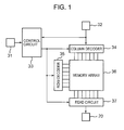
- FIG. 1 illustrates the semiconductor memory device.
- the semiconductor memory device includes a clock terminal 31, a serial input terminal 32, and a serial output terminal 20.
- the semiconductor memory device further includes a control circuit 33, a column decoder 34, a row decoder 35, a memory array 36, and a read circuit 37.
- the memory array 36 includes a plurality of memory cells.
- An input signal from the serial input terminal 32 is input to the control circuit 33 and the column decoder 34.
- a clock signal is input to the control circuit 33.
- the control circuit 33 controls the column decoder 34, the row decoder 35, and the read circuit 37.
- the column decoder 34, the row decoder 35, and the read circuit 37 are connected to the memory array 36 for each of the plurality of memory cells of the memory array 36.
- the read circuit 37 outputs data to the serial output terminal 20.
- the control circuit 33 captures the input signal from the serial input terminal 32 in synchronization with the clock signal input to the clock terminal 31.
- the input signal includes an instruction, an address, and data.
- the control circuit 33 recognizes the instruction and the address and makes an access to a predetermined memory cell of the memory array 36 corresponding to the intended address through the row decoder 35 and the column decoder 34 to select the memory cell. After that, the data is written to the memory cell.
- the control circuit 33 captures the input signal from the serial input terminal 32 in synchronization with the clock signal input to the clock terminal 31.
- the input signal includes an instruction and an address.
- the control circuit 33 recognizes the instruction and the address and makes an access to a predetermined memory cell of the memory array 36 corresponding to the intended address through the row decoder 35 and the column decoder 34 to select the memory cell. After that, the data is read from the memory cell to the read circuit 37. The data is output from the serial output terminal 20.
- FIG. 2 illustrates the read circuit.
- the read circuit 37 includes typical signal lines, that is, a bus bit line 10, bit lines bit0 to bit6, and bit lines bit7_1 to bit7_4.
- the read circuit 37 further includes byte selectors B0 to B3, switches SW0 to SW6, switches SW7_1 to SW7_4, sense amplifiers A1 to A4, latches L1 to L4, and selectors SL1 to SL5.
- the byte selectors B0 to B3 are connected to the bus bit line 10.
- the byte selector B0 includes 0th to 6th output terminals connected to the bit lines bit0 to bit6, respectively, and a 7th output terminal connected to the bit line bit7_1.
- the byte selector B1 includes 0th to 6th output terminals connected to the bit lines bit0 to bit6, respectively, and a 7th output terminal connected to the bit line bit7_2.
- the byte selector B2 includes 0th to 6th output terminals connected to the bit lines bit0 to bit6, respectively, and a 7th output terminal connected to the bit line bit7_3.
- the byte selector B3 includes 0th to 6th output terminals connected to the bit lines bit0 to bit6, respectively, and a 7th output terminal connected to the bit line bit7_4.
- the switch SW0 is provided between the bit line bit0 and an input terminal of the sense amplifier A4.
- the switch SW1 is provided between the bit line bit1 and an input terminal of the sense amplifier A3.
- the switch SW2 is provided between the bit line bit2 and the input terminal of the sense amplifier A4.
- the switch SW3 is provided between the bit line bit3 and the input terminal of the sense amplifier A3.
- the switch SW4 is provided between the bit line bit4 and the input terminal of the sense amplifier A4.
- the switch SW5 is provided between the bit line bit5 and the input terminal of the sense amplifier A3.
- the switch SW6 is provided between the bit line bit6 and an input terminal of the sense amplifier A1.
- the switch SW7_1 is provided between the bit line bit7_1 and the input terminal of the sense amplifier A1.
- the switch SW7_2 is provided between the bit line bit7_2 and an input terminal of the sense amplifier A2.
- the switch SW7_3 is provided between the bit line bit7_3 and the input terminal of the sense amplifier A3.
- the switch SW7_4 is provided between the bit line bit7_4 and the input terminal of the sense amplifier A4.
- Signals s0 to s6 are input to gates of the switches SW0 to SW6.
- Signals s7_1 to s7_4 are input to gates of the switches SW7_1 to SW7_4.
- Output terminals of the sense amplifiers A1 to A4 are connected to input terminals of the latches L1 to L4.
- a signal clk2 is input to each of clock terminals of the latches L1 to L4.
- the selector SL1 includes a first input terminal connected to an output terminal of the latch L1, a second input terminal connected to an output terminal of the latch L2, a third input terminal connected to an output terminal of the latch L3, and a fourth input terminal connected to an output terminal of the latch L4.
- the selector SL2 includes an input terminal connected to the output terminal of the sense amplifier A1.
- the selector SL3 includes an input terminal connected to the output terminal of the latch L3.
- the selector SL4 includes an input terminal connected to the output terminal of the latch L4.
- the selector SL5 includes an input terminal connected to an output terminal of the selector SL1. Signals sel1 to sel5 are input to control terminals of the selectors SL1 to SL5. Output terminals of the selectors SL2 to SL5 are connected to the serial output terminal 20.
- the byte selectors B0 to B3 each output data signals D7 to D0 from a plurality of predetermined memory cells based on an address.
- the sense amplifiers A1 to A4 simultaneously sense the respective data signals D7 from the byte selectors B0 to B3 which may be selected to determine the address before the determination of the address, simultaneously sense the data signals D6 to D4 from the byte selector corresponding to the determined address, simultaneously sense the data signals D3 and D2 from the byte selector corresponding to the determined address, and simultaneously sense the data signals D1 and D0 from the byte selector corresponding to the determined address.
- the latches L1 to L4 latch respective signals from the sense amplifiers A1 to A4. After the determination of the address, the selectors SL1 to SL5 selectively read the data signal D7 from the byte selector corresponding to the determined address, of the respective data signals D7 and sequentially selectively read the data signals D6 to D0.
- the semiconductor memory device is electrically rewritable and includes, for example, an electrically erasable programmable read only memory (EEPROM).
- EEPROM electrically erasable programmable read only memory
- FIG. 3 is a timing chart illustrating signals including data from the serial output terminal.
- the instruction is a total of eight instruction signals corresponding to eight clocks of first to eighth clock signals.
- the address is a total of 16 address signals a0 to a15 corresponding to 16 clocks of 9th to 24th clock signals.
- the data is a total of eight data signals D0 to D7 corresponding to eight clocks of 25th to 32nd clock signals.
- the instruction signals are input to the control circuit 33 in response to the eight clocks of the first to eighth clock signals. The instruction is then determined at the rising edge of the eighth clock signal.
- the address signals are input to the control circuit 33 in response to the 16 clocks of the 9th to 24th clock signals. The address is then determined at the rising edge of the 24th clock signal.
- the data signals corresponding to the address are serially read from the serial output terminal 20 at the falling edges of the 24th to 31st clock signals.
- the data signals on the bus bit line 10 are selected by the byte selectors B0 to B3 and output to the bit lines bit0 to bit6 or the bit lines bit7_1 to bit7_4.
- the control circuit 33 selects the byte selectors B0 to B3 corresponding to the four addresses.
- the byte selectors B0 to B3 output the respective data signals D7 corresponding to the four addresses to each of the bit lines bit7_1 to bit7_4.
- the control circuit 33 outputs the signals s0 to s6 and the signals s7_1 to s7_4 to turn off the switches SW0 to SW6 and turn on the switches SW7_1 to SW7_4.
- the bit lines bit7_1 to bit7_4 are connected to the input terminals of the sense amplifiers A1 to A4 through the switches SW7_1 to SW7_4. Therefore, at the rising edge of the 22nd clock signal, signals m1 to m4 input to the sense amplifiers A1 to A4 correspond to the respective data signals D7 from the byte selectors B0 to B3.
- the signals m1 to m4 (respective data signals D7 from byte selectors B0 to B3) are held until the rising edge of the 24th clock signal because the switches SW0 to SW6 continue to be turned off and the switches SW7_1 to SW7_4 continue to be turned on. Then, the signals m1 to m4 are latched as signals r1 to r4 into the latches L1 to L4 at the falling edge of the 23rd clock signal in response to the signal clk2.
- the address is determined at the rising edge of the 24th clock signal.
- the byte selector B0 corresponds to the determined address.
- the data signal D7 from the byte selector B0 (signal r1 from latch L1) is output from the serial output terminal 20 through the selectors SL1 and SL5 in response to the signals sel1 to sel5 at the falling edge of the 24th clock signal.
- the control circuit 33 After the falling edge of the 23rd clock signal, the control circuit 33 outputs the signals s0 to s6 and the signals s7_1 to s7_4 to turn on the switches SW4 to SW6 and turn off the switches SW0 to SW3 and the switches SW7_1 to SW7_4.
- bit lines bit6 to bit4 are connected to the input terminals of the sense amplifiers A1, A3, and A4 through the switches SW6 to SW4, respectively. Therefore, at the rising edge of the 24th clock signal, the signals m1, m3, and m4 input to the sense amplifiers A1, A3, and A4 correspond to the data signals D6 to D4 from the byte selector B0, respectively.
- the signals m1, m3, and m4 (data signals D6 to D4 from byte selector B0) are held until the rising edge of the 26th clock signal because the switches SW4 to SW6 continue to be turned on and the switches SW0 to SW3 and the switches SW7_1 to SW7_4 continue to be turned off. Then, the signals m1, m3, and m4 are latched as signals r1, r3, and r4 into the latches L1, L3, and L4, respectively, at the falling edge of the 25th clock signal in response to the signal clk2.
- the data signal D6 from the byte selector B0 (signal input to latch L1) is latched into the latch L1 and output from the serial output terminal 20 through the selector SL2 in response to the signal sel2.
- the data signal D5 from the byte selector B0 (signal r3 from latch L3) is output from the serial output terminal 20 through the selector SL3 in response to the signals sel1 to sel5.
- the data signal D4 from the byte selector B0 (signal r4 from latch L4) is output from the serial output terminal 20 through the selector SL4 in response to the signals sel1 to sel5.
- the control circuit 33 outputs the signals s0 to s6 and the signals s7_1 to s7_4 to turn on the switches SW2 and SW3 and turn off the switches SW0, SW1, SW4 to SW6, and SW7_1 to SW7_4.
- the bit lines bit3 and bit2 are connected to the input terminals of the sense amplifiers A3 and A4 through the switches SW3 and SW2, respectively. Therefore, at the rising edge of the 26th clock signal, the signals m3 and m4 input to the sense amplifiers A3 and A4 correspond to the data signals D3 and D2 from the byte selector B0, respectively.
- the signals m3 and m4 (data signals D3 and D2 from byte selector B0 are held until the rising edge of the 28th clock signal because the switches SW2 and SW3 continue to be turned on and the switches SW0, SW1, SW4 to SW6, and SW7_1 to SW7_4 continue to be turned off. Then, the signals m3 and m4 are latched as signals r3 and r4 into the latches L3 and L4, respectively, at the falling edge of the 27th clock signal in response to the signal clk2.
- the data signal D3 from the byte selector B0 (signal r3 from latch L3) is output from the serial output terminal 20 through the selector SL3 in response to the signals sel1 to sel5.
- the data signal D2 from the byte selector B0 (signal r4 from latch L4) is output from the serial output terminal 20 through the selector SL4 in response to the signals sel1 to sel5.
- the data signal D1 from the byte selector B0 (signal r3 from latch L3) is output from the serial output terminal 20 through the selector SL3 in response to the signals sel1 to sel5.
- the data signal D0 from the byte selector B0 (signal r4 from latch L4) is output from the serial output terminal 20 through the selector SL4 in response to the signals sel1 to sel5.
- a read processing time of each of the sense amplifiers is more likely to be longer than 1/2 of the clock signal period.
- the read processing time of each of the sense amplifiers is equal to 3/2 of the clock signal period. Therefore, the read circuit 37 and the semiconductor memory device are easily operated at high speed.
- the four byte selectors are illustrated.
- Only the byte selectors B0 to B3 corresponding to the four addresses are illustrated.
- the four sense amplifiers are provided corresponding to the byte selectors B0 to B3.
- the eight addresses correspond to eight byte selectors, and hence eight sense amplifiers may be provided corresponding to the eight byte selectors.
Landscapes
- Read Only Memory (AREA)
- Dram (AREA)
Claims (8)
- Leseschaltung (37) für eine Halbleiterspeichervorrichtung zum seriellen Lesen von Daten aus einem seriellen Ausgabeanschluss, umfassend:mehrere Byte-Selektoren (B0 - B3), jeweils zum Ausgeben erster und folgender Datensignale (D7 - D0) von mehreren vorbestimmten Speicherzellen auf der Basis einer Adresse, wobei zumindest die ersten Datensignale ausgegeben werden, bevor die Adresse bestimmt ist;mehrere Erfassungsverstärker (A1 - A4) zum gleichzeitigen Erfassen zumindest der ersten Datensignale (D7 - D0) von den mehreren Byte-Selektoren; undeine Selektorschaltung (SL1 - SD5) zum selektiven Lesen durch die mehreren Erfassungsverstärker (A1 - A4) eines der ersten Datensignale (D7), das von einem der mehreren Byte-Selektoren ausgegeben wird, der einer bestimmten Adresse entspricht, nachdem die Adresse bestimmt wurde, und sequenziellem selektiven Lesen der folgenden Datensignale (D6 - D0) aus einem der mehreren Byte-Selektoren (B0 - B3), wobei:die mehreren Byte-Selektoren (B0 - B3) jeweils zur Ausgabe erster bis achter Datensignale aus den mehreren vorbestimmten Speicherzellen auf der Basis der Adresse dienen; und wobeidie Anzahl von Erfassungsverstärkern (A1 - A4) von den mehreren Erfassungsverstärkern (A1 - A4) dieselbe ist, wie die Anzahl von Byte-Selektoren (B0 - B3) von den mehreren Byte-Selektoren (B0 - B3);die mehreren Erfassungsverstärker (A1 - A4) zum gleichzeitigen Erfassen der ersten Datensignale (D7) aus den mehreren Byte-Selektoren (B0 - B3) dienen,bevor die Adresse bestimmt ist, und zum Erfassen der zweiten bis achten Datensignale (D6 - D0) aus dem einem der mehreren Byte-Selektoren, der der bestimmten Adresse entspricht, nachdem die Adresse bestimmt wurde;die Selektorschaltung (SL1 - SL5) zum selektiven Lesen des einen der ersten Datensignale, das von dem einen der mehreren Byte-Selektoren ausgegeben wird, der der bestimmten Adresse entspricht, nachdem die Adresse bestimmt wurde, und sequenziellem selektiven Lesen der zweiten bis achten Datensignale (D6 - D0) aus dem einem der mehreren Byte-Selektoren dient; unddie mehreren Erfassungsverstärker (A1 - A4) dazu ausgebildet sind, gleichzeitig die ersten Datensignale (D7) aus den mehreren Byte-Selektoren zu erfassen,bevor die Adresse bestimmt ist, gleichzeitig die zweiten bis vierten Datensignale (D6 - D4) aus dem einen der mehreren Byte-Selektoren zu erfassen, der der bestimmten Adresse entspricht, gleichzeitig das fünfte und sechste Datensignal (D3, D2) aus dem einen der mehreren Byte-Selektoren zu erfassen, der der bestimmten Adresse entspricht, und gleichzeitig das siebente und achte Datensignal (D1, D0) aus dem einen der mehreren Byte-Selektoren zu erfassen, der der bestimmten Adresse entspricht
- Leseschaltung für eine Halbleiterspeichervorrichtung nach Anspruch 1, wobei, bevor die Adresse bestimmt wird, ein Adressensignal mit Ausnahme von zwei niederwertigen Bits von mehreren Bits, die zur Adressbestimmung notwendig sind, eingegeben wird.
- Leseschaltung für eine Halbleiterspeichervorrichtung nach einem der vorangehenden Ansprüche, wobei vier der Erfassungsverstärker (A1 - A4) vorgesehen sind.
- Leseschaltung für eine Halbleiterspeichervorrichtung nach einem der vorangehenden Ansprüche, des Weiteren umfassend mehrere Signalspeicher (L1 - L4) zum Speichern von Signalen von den mehreren Erfassungsverstärkern.
- Leseschaltung für eine Halbleiterspeichervorrichtung nach einem der vorangehenden Ansprüche, des Weiteren umfassend einen Schaltkreis (SW0 - SW6, SW7_1 - SW7_4), der zwischen den mehreren Byte-Selektoren und den mehreren Erfassungsverstärkern vorgesehen ist.
- Leseschaltung für eine Halbleiterspeichervorrichtung nach einem der vorangehenden Ansprüche, wobei die Halbleiterspeichervorrichtung elektrisch wieder beschreibbar ist.
- Leseschaltung nach Anspruch 1, wobei:die mehreren Byte-Selektoren (B0 - B3) zum Ausgeben von Daten aus zumindest zwei der Speicherzellen dienen, die in Reihen angeordnet sind, die den bestimmten Adressdaten entsprechen, bevor die Adresse bestimmt wird;die Leseschaltung des Weiteren mehrere Schaltkreise (SW0 - SW6, SW7_1 - SW7_4) umfasst, die zwischen den mehreren Byte-Selektoren und den mehreren Erfassungsverstärkern vorgesehen sind; unddie Selektorschaltung (SL1 - SL5) an die mehreren Erfassungsverstärker zum Schalten und Ausgeben von Ausgaben aus den mehreren Erfassungsverstärkern angeschlossen ist, nachdem die Adressdaten bestimmt wurden;wobei nach der Bestimmung der Adressdaten ein ersten Datensignal (D7) von einem der mehreren Byte-Selektoren, der den bestimmten Adressdaten entspricht, selektiv von einem ersten Schaltkreis der mehreren Schaltkreise gelesen wird und dann das zweite und folgende Datensignale sequenziell selektiv von den mehreren Schaltkreisen gelesen werden.
- Halbleiterspeichervorrichtung, umfassend:einen Reihendekodierer (35);einen Spaltendekodierer (34);eine Speicheranordnung (36), die mehrere Speicherzellen, die in Reihen angeordnet sind, und eine Ausgangs-Bitleitung (10) enthält, wobei zumindest eine der mehreren Speicherzellen, die sich in einer vorbestimmten Reihe befindet, von dem Reihendekodierer und Spaltendekodierer gewählt wird;eine Steuerschaltung (33), die eine Ausgangssignalleitung enthält, zum Erfassen einer Anweisung und von Adressdaten, die in einem Eingangssignal enthalten sind, und für einen Zugriff auf mindestens eine der mehreren Speicherzellen, die sich in einer Reihe befinden, entsprechend den Adressdaten durch den Reihendekodierer und Spaltendekodierer; undeine Leseschaltung (37) nach einem der vorangehenden Ansprüche, wobei die Lesesignalschaltung an die Ausgangssignalleitung der Steuerschaltung angeschlossen ist und die mehreren Byte-Selektoren an die Ausgangs-Bitleitung (10) der Speicheranordnung angeschlossen ist für eine serielle Ausgabe von Daten aus der zumindest einen der mehreren Speicherzellen, die sich in der Reihe befinden, die den Adressdaten entspricht.
Applications Claiming Priority (1)
| Application Number | Priority Date | Filing Date | Title |
|---|---|---|---|
| JP2008289480A JP5291437B2 (ja) | 2008-11-12 | 2008-11-12 | 半導体記憶装置の読出回路及び半導体記憶装置 |
Publications (2)
| Publication Number | Publication Date |
|---|---|
| EP2187399A1 EP2187399A1 (de) | 2010-05-19 |
| EP2187399B1 true EP2187399B1 (de) | 2012-07-18 |
Family
ID=41650330
Family Applications (1)
| Application Number | Title | Priority Date | Filing Date |
|---|---|---|---|
| EP09175332A Not-in-force EP2187399B1 (de) | 2008-11-12 | 2009-11-06 | Leseschaltung für eine Halbleiterspeichervorrichtung und Halbleiterspeichervorrichtung |
Country Status (6)
| Country | Link |
|---|---|
| US (1) | US8218388B2 (de) |
| EP (1) | EP2187399B1 (de) |
| JP (1) | JP5291437B2 (de) |
| KR (1) | KR101268652B1 (de) |
| CN (1) | CN101740098B (de) |
| TW (1) | TWI494938B (de) |
Families Citing this family (7)
| Publication number | Priority date | Publication date | Assignee | Title |
|---|---|---|---|---|
| JP5319572B2 (ja) * | 2010-02-23 | 2013-10-16 | セミコンダクター・コンポーネンツ・インダストリーズ・リミテッド・ライアビリティ・カンパニー | メモリ装置 |
| CN103544991B (zh) * | 2012-07-12 | 2016-06-22 | 华邦电子股份有限公司 | 闪存装置及其操作的方法 |
| CN108459983B (zh) * | 2017-02-22 | 2021-04-02 | 致茂电子(苏州)有限公司 | 可程序化信号传输方法 |
| US11398271B2 (en) | 2019-12-30 | 2022-07-26 | Taiwan Semiconductor Manufacturing Company, Ltd. | Memory device having a comparator circuit |
| DE102020130253A1 (de) * | 2019-12-30 | 2021-07-01 | Taiwan Semiconductor Manufacturing Co., Ltd. | Speichervorrichtung |
| CN114692558B (zh) * | 2020-12-29 | 2025-12-05 | 格科微电子(上海)有限公司 | 基于3d封装的集成电路 |
| CN112542193B (zh) * | 2020-12-30 | 2023-07-25 | 芯天下技术股份有限公司 | 一种高速读取数据的spi接口的flash存储器 |
Family Cites Families (9)
| Publication number | Priority date | Publication date | Assignee | Title |
|---|---|---|---|---|
| JP3112021B2 (ja) * | 1990-07-09 | 2000-11-27 | 株式会社日立製作所 | 半導体メモリ |
| JPH06111572A (ja) * | 1992-09-29 | 1994-04-22 | Nec Corp | 半導体記憶装置 |
| FR2726934B1 (fr) * | 1994-11-10 | 1997-01-17 | Sgs Thomson Microelectronics | Procede de lecture anticipee de memoire a acces serie et memoire s'y rapportant |
| JP3317187B2 (ja) * | 1997-04-25 | 2002-08-26 | 日本電気株式会社 | 半導体記憶装置 |
| JPH11288594A (ja) * | 1998-03-31 | 1999-10-19 | Asahi Kasei Micro Syst Co Ltd | 半導体記憶装置 |
| US6038185A (en) * | 1998-05-12 | 2000-03-14 | Atmel Corporation | Method and apparatus for a serial access memory |
| JP2002216483A (ja) * | 2001-01-18 | 2002-08-02 | Toshiba Corp | 半導体記憶装置 |
| JP2002251886A (ja) * | 2001-02-22 | 2002-09-06 | Seiko Instruments Inc | シリアル入出力メモリ |
| US7529149B2 (en) * | 2006-12-12 | 2009-05-05 | Mosaid Technologies Incorporated | Memory system and method with serial and parallel modes |
-
2008
- 2008-11-12 JP JP2008289480A patent/JP5291437B2/ja active Active
-
2009
- 2009-11-04 TW TW098137398A patent/TWI494938B/zh active
- 2009-11-06 EP EP09175332A patent/EP2187399B1/de not_active Not-in-force
- 2009-11-09 US US12/614,909 patent/US8218388B2/en not_active Expired - Fee Related
- 2009-11-11 KR KR1020090108677A patent/KR101268652B1/ko active Active
- 2009-11-12 CN CN200910225288.1A patent/CN101740098B/zh active Active
Also Published As
| Publication number | Publication date |
|---|---|
| EP2187399A1 (de) | 2010-05-19 |
| CN101740098B (zh) | 2016-03-30 |
| KR101268652B1 (ko) | 2013-05-29 |
| JP2010118102A (ja) | 2010-05-27 |
| US20100118624A1 (en) | 2010-05-13 |
| JP5291437B2 (ja) | 2013-09-18 |
| CN101740098A (zh) | 2010-06-16 |
| TW201025350A (en) | 2010-07-01 |
| US8218388B2 (en) | 2012-07-10 |
| KR20100053472A (ko) | 2010-05-20 |
| TWI494938B (zh) | 2015-08-01 |
Similar Documents
| Publication | Publication Date | Title |
|---|---|---|
| EP2187399B1 (de) | Leseschaltung für eine Halbleiterspeichervorrichtung und Halbleiterspeichervorrichtung | |
| US7808825B2 (en) | Non-volatile memory device and method of programming the same | |
| KR101036727B1 (ko) | I2c 어드레싱의 방법 및 이를 수행하기 위한 디바이스 | |
| US6965964B2 (en) | Nand flash memory device | |
| CN112634960B (zh) | 存储器及其寻址方法 | |
| CN111627481A (zh) | 一种字线译码电路、字线选通方法及存储器和电子设备 | |
| US7051153B1 (en) | Memory array operating as a shift register | |
| US6282136B1 (en) | Semiconductor memory devices and sensors using the same | |
| EP1335386B1 (de) | Schieberegister | |
| US20100226172A1 (en) | Method of reading data and method of inputting and outputting data in non-volatile memory device | |
| CN110349605B (zh) | 通道控制装置 | |
| KR20040093817A (ko) | 초기화 동작시간이 감소된 태그블럭을 구비하는 반도체메모리 장치 | |
| KR20160093548A (ko) | 반도체 기억 장치 및 데이터 기입 방법 | |
| KR100305083B1 (ko) | 배선전환회로를구비한반도체장치 | |
| US7075846B2 (en) | Apparatus for interleave and method thereof | |
| JP3600233B2 (ja) | 信号処理装置 | |
| EP3460799B1 (de) | Halbleiterspeichervorrichtung und verfahren zur steuerung einer halbleiterspeichervorrichtung | |
| CN114756487A (zh) | 一种串行eeprom的型号识别及控制器设计方法 | |
| JP3600234B2 (ja) | オーディオ装置 | |
| KR100624286B1 (ko) | 플래시 메모리의 리페어 장치 | |
| JP2008165887A (ja) | メモリリード回路、それを用いたメモリ装置 | |
| KR100399923B1 (ko) | 코드 및 데이터 저장용 플래쉬 메모리 장치 | |
| CN117724600A (zh) | 读写控制电路及读写控制方法 | |
| KR20080088172A (ko) | 더블 데이터 레이트 낸드 플래시 메모리 장치 | |
| KR19990003406A (ko) | 다중 레벨 셀들을 갖는 메모리 장치 및 그것의 데이터 기입 방법 |
Legal Events
| Date | Code | Title | Description |
|---|---|---|---|
| PUAI | Public reference made under article 153(3) epc to a published international application that has entered the european phase |
Free format text: ORIGINAL CODE: 0009012 |
|
| AK | Designated contracting states |
Kind code of ref document: A1 Designated state(s): AT BE BG CH CY CZ DE DK EE ES FI FR GB GR HR HU IE IS IT LI LT LU LV MC MK MT NL NO PL PT RO SE SI SK SM TR |
|
| AX | Request for extension of the european patent |
Extension state: AL BA RS |
|
| 17P | Request for examination filed |
Effective date: 20101119 |
|
| 17Q | First examination report despatched |
Effective date: 20110107 |
|
| GRAP | Despatch of communication of intention to grant a patent |
Free format text: ORIGINAL CODE: EPIDOSNIGR1 |
|
| GRAS | Grant fee paid |
Free format text: ORIGINAL CODE: EPIDOSNIGR3 |
|
| GRAA | (expected) grant |
Free format text: ORIGINAL CODE: 0009210 |
|
| AK | Designated contracting states |
Kind code of ref document: B1 Designated state(s): AT BE BG CH CY CZ DE DK EE ES FI FR GB GR HR HU IE IS IT LI LT LU LV MC MK MT NL NO PL PT RO SE SI SK SM TR |
|
| REG | Reference to a national code |
Ref country code: GB Ref legal event code: FG4D |
|
| REG | Reference to a national code |
Ref country code: CH Ref legal event code: EP |
|
| REG | Reference to a national code |
Ref country code: AT Ref legal event code: REF Ref document number: 567192 Country of ref document: AT Kind code of ref document: T Effective date: 20120815 Ref country code: IE Ref legal event code: FG4D |
|
| REG | Reference to a national code |
Ref country code: DE Ref legal event code: R096 Ref document number: 602009008343 Country of ref document: DE Effective date: 20120913 |
|
| REG | Reference to a national code |
Ref country code: NL Ref legal event code: VDEP Effective date: 20120718 |
|
| REG | Reference to a national code |
Ref country code: AT Ref legal event code: MK05 Ref document number: 567192 Country of ref document: AT Kind code of ref document: T Effective date: 20120718 |
|
| REG | Reference to a national code |
Ref country code: LT Ref legal event code: MG4D Effective date: 20120718 |
|
| PG25 | Lapsed in a contracting state [announced via postgrant information from national office to epo] |
Ref country code: FI Free format text: LAPSE BECAUSE OF FAILURE TO SUBMIT A TRANSLATION OF THE DESCRIPTION OR TO PAY THE FEE WITHIN THE PRESCRIBED TIME-LIMIT Effective date: 20120718 Ref country code: HR Free format text: LAPSE BECAUSE OF FAILURE TO SUBMIT A TRANSLATION OF THE DESCRIPTION OR TO PAY THE FEE WITHIN THE PRESCRIBED TIME-LIMIT Effective date: 20120718 Ref country code: LT Free format text: LAPSE BECAUSE OF FAILURE TO SUBMIT A TRANSLATION OF THE DESCRIPTION OR TO PAY THE FEE WITHIN THE PRESCRIBED TIME-LIMIT Effective date: 20120718 Ref country code: BE Free format text: LAPSE BECAUSE OF FAILURE TO SUBMIT A TRANSLATION OF THE DESCRIPTION OR TO PAY THE FEE WITHIN THE PRESCRIBED TIME-LIMIT Effective date: 20120718 Ref country code: IS Free format text: LAPSE BECAUSE OF FAILURE TO SUBMIT A TRANSLATION OF THE DESCRIPTION OR TO PAY THE FEE WITHIN THE PRESCRIBED TIME-LIMIT Effective date: 20121118 Ref country code: NO Free format text: LAPSE BECAUSE OF FAILURE TO SUBMIT A TRANSLATION OF THE DESCRIPTION OR TO PAY THE FEE WITHIN THE PRESCRIBED TIME-LIMIT Effective date: 20121018 Ref country code: CY Free format text: LAPSE BECAUSE OF FAILURE TO SUBMIT A TRANSLATION OF THE DESCRIPTION OR TO PAY THE FEE WITHIN THE PRESCRIBED TIME-LIMIT Effective date: 20120718 Ref country code: AT Free format text: LAPSE BECAUSE OF FAILURE TO SUBMIT A TRANSLATION OF THE DESCRIPTION OR TO PAY THE FEE WITHIN THE PRESCRIBED TIME-LIMIT Effective date: 20120718 |
|
| PG25 | Lapsed in a contracting state [announced via postgrant information from national office to epo] |
Ref country code: SI Free format text: LAPSE BECAUSE OF FAILURE TO SUBMIT A TRANSLATION OF THE DESCRIPTION OR TO PAY THE FEE WITHIN THE PRESCRIBED TIME-LIMIT Effective date: 20120718 Ref country code: PT Free format text: LAPSE BECAUSE OF FAILURE TO SUBMIT A TRANSLATION OF THE DESCRIPTION OR TO PAY THE FEE WITHIN THE PRESCRIBED TIME-LIMIT Effective date: 20121119 Ref country code: PL Free format text: LAPSE BECAUSE OF FAILURE TO SUBMIT A TRANSLATION OF THE DESCRIPTION OR TO PAY THE FEE WITHIN THE PRESCRIBED TIME-LIMIT Effective date: 20120718 Ref country code: LV Free format text: LAPSE BECAUSE OF FAILURE TO SUBMIT A TRANSLATION OF THE DESCRIPTION OR TO PAY THE FEE WITHIN THE PRESCRIBED TIME-LIMIT Effective date: 20120718 Ref country code: SE Free format text: LAPSE BECAUSE OF FAILURE TO SUBMIT A TRANSLATION OF THE DESCRIPTION OR TO PAY THE FEE WITHIN THE PRESCRIBED TIME-LIMIT Effective date: 20120718 Ref country code: GR Free format text: LAPSE BECAUSE OF FAILURE TO SUBMIT A TRANSLATION OF THE DESCRIPTION OR TO PAY THE FEE WITHIN THE PRESCRIBED TIME-LIMIT Effective date: 20121019 |
|
| PG25 | Lapsed in a contracting state [announced via postgrant information from national office to epo] |
Ref country code: NL Free format text: LAPSE BECAUSE OF FAILURE TO SUBMIT A TRANSLATION OF THE DESCRIPTION OR TO PAY THE FEE WITHIN THE PRESCRIBED TIME-LIMIT Effective date: 20120718 |
|
| PG25 | Lapsed in a contracting state [announced via postgrant information from national office to epo] |
Ref country code: EE Free format text: LAPSE BECAUSE OF FAILURE TO SUBMIT A TRANSLATION OF THE DESCRIPTION OR TO PAY THE FEE WITHIN THE PRESCRIBED TIME-LIMIT Effective date: 20120718 Ref country code: CZ Free format text: LAPSE BECAUSE OF FAILURE TO SUBMIT A TRANSLATION OF THE DESCRIPTION OR TO PAY THE FEE WITHIN THE PRESCRIBED TIME-LIMIT Effective date: 20120718 Ref country code: DK Free format text: LAPSE BECAUSE OF FAILURE TO SUBMIT A TRANSLATION OF THE DESCRIPTION OR TO PAY THE FEE WITHIN THE PRESCRIBED TIME-LIMIT Effective date: 20120718 Ref country code: RO Free format text: LAPSE BECAUSE OF FAILURE TO SUBMIT A TRANSLATION OF THE DESCRIPTION OR TO PAY THE FEE WITHIN THE PRESCRIBED TIME-LIMIT Effective date: 20120718 Ref country code: ES Free format text: LAPSE BECAUSE OF FAILURE TO SUBMIT A TRANSLATION OF THE DESCRIPTION OR TO PAY THE FEE WITHIN THE PRESCRIBED TIME-LIMIT Effective date: 20121029 |
|
| PLBE | No opposition filed within time limit |
Free format text: ORIGINAL CODE: 0009261 |
|
| STAA | Information on the status of an ep patent application or granted ep patent |
Free format text: STATUS: NO OPPOSITION FILED WITHIN TIME LIMIT |
|
| PG25 | Lapsed in a contracting state [announced via postgrant information from national office to epo] |
Ref country code: IT Free format text: LAPSE BECAUSE OF FAILURE TO SUBMIT A TRANSLATION OF THE DESCRIPTION OR TO PAY THE FEE WITHIN THE PRESCRIBED TIME-LIMIT Effective date: 20120718 Ref country code: SK Free format text: LAPSE BECAUSE OF FAILURE TO SUBMIT A TRANSLATION OF THE DESCRIPTION OR TO PAY THE FEE WITHIN THE PRESCRIBED TIME-LIMIT Effective date: 20120718 |
|
| 26N | No opposition filed |
Effective date: 20130419 |
|
| PG25 | Lapsed in a contracting state [announced via postgrant information from national office to epo] |
Ref country code: BG Free format text: LAPSE BECAUSE OF FAILURE TO SUBMIT A TRANSLATION OF THE DESCRIPTION OR TO PAY THE FEE WITHIN THE PRESCRIBED TIME-LIMIT Effective date: 20121018 |
|
| REG | Reference to a national code |
Ref country code: DE Ref legal event code: R097 Ref document number: 602009008343 Country of ref document: DE Effective date: 20130419 Ref country code: IE Ref legal event code: MM4A |
|
| PG25 | Lapsed in a contracting state [announced via postgrant information from national office to epo] |
Ref country code: IE Free format text: LAPSE BECAUSE OF NON-PAYMENT OF DUE FEES Effective date: 20121106 |
|
| PG25 | Lapsed in a contracting state [announced via postgrant information from national office to epo] |
Ref country code: MT Free format text: LAPSE BECAUSE OF FAILURE TO SUBMIT A TRANSLATION OF THE DESCRIPTION OR TO PAY THE FEE WITHIN THE PRESCRIBED TIME-LIMIT Effective date: 20120718 |
|
| PG25 | Lapsed in a contracting state [announced via postgrant information from national office to epo] |
Ref country code: MC Free format text: LAPSE BECAUSE OF NON-PAYMENT OF DUE FEES Effective date: 20121130 Ref country code: TR Free format text: LAPSE BECAUSE OF FAILURE TO SUBMIT A TRANSLATION OF THE DESCRIPTION OR TO PAY THE FEE WITHIN THE PRESCRIBED TIME-LIMIT Effective date: 20120718 |
|
| PG25 | Lapsed in a contracting state [announced via postgrant information from national office to epo] |
Ref country code: SM Free format text: LAPSE BECAUSE OF FAILURE TO SUBMIT A TRANSLATION OF THE DESCRIPTION OR TO PAY THE FEE WITHIN THE PRESCRIBED TIME-LIMIT Effective date: 20120718 Ref country code: LU Free format text: LAPSE BECAUSE OF NON-PAYMENT OF DUE FEES Effective date: 20121106 |
|
| REG | Reference to a national code |
Ref country code: CH Ref legal event code: PL |
|
| GBPC | Gb: european patent ceased through non-payment of renewal fee |
Effective date: 20131106 |
|
| PG25 | Lapsed in a contracting state [announced via postgrant information from national office to epo] |
Ref country code: HU Free format text: LAPSE BECAUSE OF FAILURE TO SUBMIT A TRANSLATION OF THE DESCRIPTION OR TO PAY THE FEE WITHIN THE PRESCRIBED TIME-LIMIT Effective date: 20091106 Ref country code: CH Free format text: LAPSE BECAUSE OF NON-PAYMENT OF DUE FEES Effective date: 20131130 Ref country code: LI Free format text: LAPSE BECAUSE OF NON-PAYMENT OF DUE FEES Effective date: 20131130 |
|
| PG25 | Lapsed in a contracting state [announced via postgrant information from national office to epo] |
Ref country code: GB Free format text: LAPSE BECAUSE OF NON-PAYMENT OF DUE FEES Effective date: 20131106 |
|
| PG25 | Lapsed in a contracting state [announced via postgrant information from national office to epo] |
Ref country code: MK Free format text: LAPSE BECAUSE OF FAILURE TO SUBMIT A TRANSLATION OF THE DESCRIPTION OR TO PAY THE FEE WITHIN THE PRESCRIBED TIME-LIMIT Effective date: 20120718 |
|
| REG | Reference to a national code |
Ref country code: FR Ref legal event code: PLFP Year of fee payment: 7 |
|
| REG | Reference to a national code |
Ref country code: DE Ref legal event code: R081 Ref document number: 602009008343 Country of ref document: DE Owner name: SII SEMICONDUCTOR CORPORATION, CHIBA-SHI, JP Free format text: FORMER OWNER: SEIKO INSTRUMENTS INC., CHIBA, JP Ref country code: DE Ref legal event code: R081 Ref document number: 602009008343 Country of ref document: DE Owner name: ABLIC INC., JP Free format text: FORMER OWNER: SEIKO INSTRUMENTS INC., CHIBA, JP |
|
| REG | Reference to a national code |
Ref country code: FR Ref legal event code: TP Owner name: SII SEMICONDUCTOR CORPORATION, JP Effective date: 20160603 |
|
| REG | Reference to a national code |
Ref country code: FR Ref legal event code: PLFP Year of fee payment: 8 |
|
| REG | Reference to a national code |
Ref country code: FR Ref legal event code: PLFP Year of fee payment: 9 |
|
| REG | Reference to a national code |
Ref country code: DE Ref legal event code: R081 Ref document number: 602009008343 Country of ref document: DE Owner name: ABLIC INC., JP Free format text: FORMER OWNER: SII SEMICONDUCTOR CORPORATION, CHIBA-SHI, CHIBA-KEN, JP |
|
| REG | Reference to a national code |
Ref country code: FR Ref legal event code: PLFP Year of fee payment: 10 |
|
| PGFP | Annual fee paid to national office [announced via postgrant information from national office to epo] |
Ref country code: DE Payment date: 20210929 Year of fee payment: 13 |
|
| PGFP | Annual fee paid to national office [announced via postgrant information from national office to epo] |
Ref country code: FR Payment date: 20211018 Year of fee payment: 13 |
|
| REG | Reference to a national code |
Ref country code: DE Ref legal event code: R119 Ref document number: 602009008343 Country of ref document: DE |
|
| PG25 | Lapsed in a contracting state [announced via postgrant information from national office to epo] |
Ref country code: DE Free format text: LAPSE BECAUSE OF NON-PAYMENT OF DUE FEES Effective date: 20230601 |
|
| PG25 | Lapsed in a contracting state [announced via postgrant information from national office to epo] |
Ref country code: FR Free format text: LAPSE BECAUSE OF NON-PAYMENT OF DUE FEES Effective date: 20221130 |