JP3600233B2 - 信号処理装置 - Google Patents
信号処理装置 Download PDFInfo
- Publication number
- JP3600233B2 JP3600233B2 JP2004017406A JP2004017406A JP3600233B2 JP 3600233 B2 JP3600233 B2 JP 3600233B2 JP 2004017406 A JP2004017406 A JP 2004017406A JP 2004017406 A JP2004017406 A JP 2004017406A JP 3600233 B2 JP3600233 B2 JP 3600233B2
- Authority
- JP
- Japan
- Prior art keywords
- signal
- output
- signal processing
- processing device
- data
- Prior art date
- Legal status (The legal status is an assumption and is not a legal conclusion. Google has not performed a legal analysis and makes no representation as to the accuracy of the status listed.)
- Expired - Lifetime
Links
Images




Landscapes
- Analogue/Digital Conversion (AREA)
Description
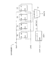
31 信号処理装置(シリアル/パラレル変換器)
41 デジタル信号処理回路
42 デジタル/アナログ変換器
43 伸長信号処理回路
44 デジタル/アナログ変換部
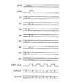
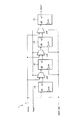
CNT1 2ビットカウンタ
CNT2 3ビットカウンタ
D1〜D4 入力端子
DEC1,DEC2 デコード回路(選択手段)
F1〜F4 ANDゲート(選択手段)
G;G1〜G4 クロック入力端子
INV インバータ(選択手段)
Q1〜Q4 出力端子
R1〜R4 レジスタ(記憶素子)
S1,S2 セレクタ(選択手段)
μCOM 制御マイコン(選択手段)
Claims (1)
- 予め定めるデータ単位のビット数分の記憶素子を備える記憶素子群と、
前記各記憶素子を予め定める順に個別に選択してゆき、選択された記憶素子から信号を順次出力させる選択手段とを備え、
前記選択手段が、カウンタと、前記カウンタのカウント値に応じて前記各記憶素子を選択していゆくセレクタとを備える信号処理装置において、
所定数の信号転送区間が設定されており、
前記カウンタが冗長または空白ビットを用いることにより、前記セレクタが前記信号転送区間の前詰め出力と後詰め出力との切換えを行うことを特徴とする信号処理装置。
Priority Applications (1)
| Application Number | Priority Date | Filing Date | Title |
|---|---|---|---|
| JP2004017406A JP3600233B2 (ja) | 2004-01-26 | 2004-01-26 | 信号処理装置 |
Applications Claiming Priority (1)
| Application Number | Priority Date | Filing Date | Title |
|---|---|---|---|
| JP2004017406A JP3600233B2 (ja) | 2004-01-26 | 2004-01-26 | 信号処理装置 |
Related Parent Applications (1)
| Application Number | Title | Priority Date | Filing Date |
|---|---|---|---|
| JP2000124848A Division JP2001308719A (ja) | 2000-04-25 | 2000-04-25 | 信号処理装置 |
Publications (2)
| Publication Number | Publication Date |
|---|---|
| JP2004147353A JP2004147353A (ja) | 2004-05-20 |
| JP3600233B2 true JP3600233B2 (ja) | 2004-12-15 |
Family
ID=32464203
Family Applications (1)
| Application Number | Title | Priority Date | Filing Date |
|---|---|---|---|
| JP2004017406A Expired - Lifetime JP3600233B2 (ja) | 2004-01-26 | 2004-01-26 | 信号処理装置 |
Country Status (1)
| Country | Link |
|---|---|
| JP (1) | JP3600233B2 (ja) |
Families Citing this family (1)
| Publication number | Priority date | Publication date | Assignee | Title |
|---|---|---|---|---|
| JP4517891B2 (ja) * | 2005-02-28 | 2010-08-04 | 日本電気株式会社 | シリアル/パラレル変換回路及びパラレル/シリアル変換回路 |
-
2004
- 2004-01-26 JP JP2004017406A patent/JP3600233B2/ja not_active Expired - Lifetime
Also Published As
| Publication number | Publication date |
|---|---|
| JP2004147353A (ja) | 2004-05-20 |
Similar Documents
| Publication | Publication Date | Title |
|---|---|---|
| KR100383421B1 (ko) | 메모리 제어 회로 | |
| JPS59157811A (ja) | デ−タ補間回路 | |
| EP2187399B1 (en) | Read circuit for semiconductor memory device and semiconductor memory device | |
| US7051153B1 (en) | Memory array operating as a shift register | |
| JP2566206B2 (ja) | 逐次近似レジスタ | |
| JP2000156092A (ja) | 同期式バースト不揮発性半導体記憶装置 | |
| JP3600233B2 (ja) | 信号処理装置 | |
| JP3600234B2 (ja) | オーディオ装置 | |
| JP2001308719A (ja) | 信号処理装置 | |
| US20080117710A1 (en) | Look-up table cascade circuit, look-up table cascade array circuit and a pipeline control method thereof | |
| JP2000304831A (ja) | テスト回路 | |
| JP3909509B2 (ja) | シリアルインタフェース回路 | |
| KR100671355B1 (ko) | 입력 회로 및 그 입력 회로를 이용하는 반도체 장치 | |
| US8327108B2 (en) | Slave and a master device, a system incorporating the devices, and a method of operating the slave device | |
| JP4129280B2 (ja) | バレルシフト装置 | |
| JP4510498B2 (ja) | 半導体集積回路 | |
| TWI575384B (zh) | 通道控制裝置 | |
| JP3288262B2 (ja) | データインタリーブ回路 | |
| JP2002005994A (ja) | 半導体装置のテスト回路 | |
| KR100200489B1 (ko) | 데이타 인터페이스 장치 | |
| JP4682786B2 (ja) | マイクロコンピュータ | |
| JP4973042B2 (ja) | データ位置変換装置およびデータ位置変換方法 | |
| JP2007304073A (ja) | 半導体装置および半導体装置のテスト実行方法 | |
| JPH01314023A (ja) | ディジタル信号処理回路 | |
| JP2001167570A (ja) | ラインメモリ装置 |
Legal Events
| Date | Code | Title | Description |
|---|---|---|---|
| A131 | Notification of reasons for refusal |
Free format text: JAPANESE INTERMEDIATE CODE: A131 Effective date: 20040622 |
|
| A521 | Written amendment |
Free format text: JAPANESE INTERMEDIATE CODE: A523 Effective date: 20040823 |
|
| TRDD | Decision of grant or rejection written | ||
| A01 | Written decision to grant a patent or to grant a registration (utility model) |
Free format text: JAPANESE INTERMEDIATE CODE: A01 Effective date: 20040914 |
|
| A61 | First payment of annual fees (during grant procedure) |
Free format text: JAPANESE INTERMEDIATE CODE: A61 Effective date: 20040915 |
|
| R150 | Certificate of patent (=grant) or registration of utility model |
Free format text: JAPANESE INTERMEDIATE CODE: R150 |
|
| FPAY | Renewal fee payment (prs date is renewal date of database) |
Free format text: PAYMENT UNTIL: 20080924 Year of fee payment: 4 |
|
| FPAY | Renewal fee payment (prs date is renewal date of database) |
Free format text: PAYMENT UNTIL: 20080924 Year of fee payment: 4 |
|
| FPAY | Renewal fee payment (prs date is renewal date of database) |
Free format text: PAYMENT UNTIL: 20090924 Year of fee payment: 5 |
|
| FPAY | Renewal fee payment (prs date is renewal date of database) |
Free format text: PAYMENT UNTIL: 20090924 Year of fee payment: 5 |
|
| FPAY | Renewal fee payment (prs date is renewal date of database) |
Free format text: PAYMENT UNTIL: 20100924 Year of fee payment: 6 |
|
| FPAY | Renewal fee payment (prs date is renewal date of database) |
Free format text: PAYMENT UNTIL: 20110924 Year of fee payment: 7 |
|
| FPAY | Renewal fee payment (prs date is renewal date of database) |
Free format text: PAYMENT UNTIL: 20120924 Year of fee payment: 8 |