EP2187452A2 - Procédé de marquage/codage d'une cellule solaire et cellule solaire - Google Patents
Procédé de marquage/codage d'une cellule solaire et cellule solaire Download PDFInfo
- Publication number
- EP2187452A2 EP2187452A2 EP09174084A EP09174084A EP2187452A2 EP 2187452 A2 EP2187452 A2 EP 2187452A2 EP 09174084 A EP09174084 A EP 09174084A EP 09174084 A EP09174084 A EP 09174084A EP 2187452 A2 EP2187452 A2 EP 2187452A2
- Authority
- EP
- European Patent Office
- Prior art keywords
- coding
- solar cell
- electrode finger
- electrode fingers
- electrode
- Prior art date
- Legal status (The legal status is an assumption and is not a legal conclusion. Google has not performed a legal analysis and makes no representation as to the accuracy of the status listed.)
- Withdrawn
Links
Images

Classifications
-
- H—ELECTRICITY
- H10—SEMICONDUCTOR DEVICES; ELECTRIC SOLID-STATE DEVICES NOT OTHERWISE PROVIDED FOR
- H10F—INORGANIC SEMICONDUCTOR DEVICES SENSITIVE TO INFRARED RADIATION, LIGHT, ELECTROMAGNETIC RADIATION OF SHORTER WAVELENGTH OR CORPUSCULAR RADIATION
- H10F71/00—Manufacture or treatment of devices covered by this subclass
-
- H—ELECTRICITY
- H10—SEMICONDUCTOR DEVICES; ELECTRIC SOLID-STATE DEVICES NOT OTHERWISE PROVIDED FOR
- H10F—INORGANIC SEMICONDUCTOR DEVICES SENSITIVE TO INFRARED RADIATION, LIGHT, ELECTROMAGNETIC RADIATION OF SHORTER WAVELENGTH OR CORPUSCULAR RADIATION
- H10F77/00—Constructional details of devices covered by this subclass
- H10F77/20—Electrodes
- H10F77/206—Electrodes for devices having potential barriers
- H10F77/211—Electrodes for devices having potential barriers for photovoltaic cells
- H10F77/215—Geometries of grid contacts
-
- H—ELECTRICITY
- H10—SEMICONDUCTOR DEVICES; ELECTRIC SOLID-STATE DEVICES NOT OTHERWISE PROVIDED FOR
- H10W—GENERIC PACKAGES, INTERCONNECTIONS, CONNECTORS OR OTHER CONSTRUCTIONAL DETAILS OF DEVICES COVERED BY CLASS H10
- H10W46/00—Marks applied to devices, e.g. for alignment or identification
-
- H—ELECTRICITY
- H10—SEMICONDUCTOR DEVICES; ELECTRIC SOLID-STATE DEVICES NOT OTHERWISE PROVIDED FOR
- H10W—GENERIC PACKAGES, INTERCONNECTIONS, CONNECTORS OR OTHER CONSTRUCTIONAL DETAILS OF DEVICES COVERED BY CLASS H10
- H10W46/00—Marks applied to devices, e.g. for alignment or identification
- H10W46/401—Marks applied to devices, e.g. for alignment or identification for identification or tracking
-
- H—ELECTRICITY
- H10—SEMICONDUCTOR DEVICES; ELECTRIC SOLID-STATE DEVICES NOT OTHERWISE PROVIDED FOR
- H10W—GENERIC PACKAGES, INTERCONNECTIONS, CONNECTORS OR OTHER CONSTRUCTIONAL DETAILS OF DEVICES COVERED BY CLASS H10
- H10W46/00—Marks applied to devices, e.g. for alignment or identification
- H10W46/601—Marks applied to devices, e.g. for alignment or identification for use after dicing
- H10W46/603—Formed on wafers or substrates before dicing and remaining on chips after dicing
-
- Y—GENERAL TAGGING OF NEW TECHNOLOGICAL DEVELOPMENTS; GENERAL TAGGING OF CROSS-SECTIONAL TECHNOLOGIES SPANNING OVER SEVERAL SECTIONS OF THE IPC; TECHNICAL SUBJECTS COVERED BY FORMER USPC CROSS-REFERENCE ART COLLECTIONS [XRACs] AND DIGESTS
- Y02—TECHNOLOGIES OR APPLICATIONS FOR MITIGATION OR ADAPTATION AGAINST CLIMATE CHANGE
- Y02E—REDUCTION OF GREENHOUSE GAS [GHG] EMISSIONS, RELATED TO ENERGY GENERATION, TRANSMISSION OR DISTRIBUTION
- Y02E10/00—Energy generation through renewable energy sources
- Y02E10/50—Photovoltaic [PV] energy
Definitions
- the invention relates to a method for marking or coding a solar cell and a solar cell.
- markings are usually applied to the visible surfaces of the solar cells, which identify the respective manufacturer. This makes it possible, in case of malfunction of a solar cell, to determine the responsible manufacturer at a glance. In addition, it may be necessary to mark different types of solar cells of the same manufacturer with different markings, for example, to prevent confusion when assembling modules from different solar cell types.
- a mark e.g., manufacturer's logo
- additional coding e.g. of the solar cell type by means of alphanumeric markings avoided.
- Such markings also have the disadvantage that the solar cell areas occupied by them are not available for the conversion of light into solar power due to shading or other impairments. In addition, additional materials and possibly further work steps are needed for the markings.
- the invention is based on the consideration of using the electrode fingers or grid fingers for the marking of the solar cell, which are applied in any case on the surface of the solar cell, in particular in front-contacted solar cells, in order to ensure their function.
- the geometric and / or optical properties of the electrode fingers are chosen so that they can represent an encoded number, and at the same time their functionality for current extraction from the solar cell and / or current transmission maintained.
- the license plate is first converted into a number, which is coded in a place value system.
- the significance system can be, for example, a binary system, a ternary system or the like.
- This number is then introduced into the electrode finger pattern on the surface of the solar cell in such a way that the number can be read from the geometric and / or optical properties of the electrode fingers.
- These properties used for the coding of the number are to be selected so that they have no or only a small, ideally negligible, influence on the functionality of the electrode fingers as current collecting elements for the solar cell.
- the geometric and / or optical properties may include properties that are optically readable.
- geometric Properties include thickness, width, length, orientation and position of an electrode finger as well as the distance between several electrode fingers.
- optical properties such as, for example, the reflexivity of an electrode finger and its permeability or its absorption capacity for electromagnetic radiation, for example in the visible, infrared or ultraviolet range, are also suitable for this purpose.
- conductor sections on the solar cell surface which are stretched in their direction of extent and are provided for removing, collecting and / or forwarding the solar cell generated currents, thus also shorter connecting pieces which are longer than bridge elements, usually over almost the connect the entire width of the surface extending conductor sections together.
- This geometric and / or optical property, which identifies the solar cell is preferably a characteristic deviating from the other electrode fingers of the electrode finger pattern, for example an offset relative to adjacent electrode fingers or an increased or reduced electrode width compared to the other electrode fingers.
- the marking electrode finger fulfills the same electrical functions as the non-marking electrode fingers and only additionally by its position on the substrate surface or other geometric and / or optical properties of the solar cell, for example, as belonging to a specific series type.
- a solar cell with the following features is disclosed.
- the solar cell has a surface with an electrode finger pattern applied to the surface with a plurality of electrically conductive electrode fingers, wherein at least one electrically conductive electrode finger is designed as a coding electrode finger, in that the encoding electrode finger comprises geometric and / or optical properties that represent a characteristic of the solar cell. Characteristics can be all conceivable properties of the solar cell. Examples of an indicator are the serial type of the cell, defined functional properties for specific applications or operating scenarios. A preferred variant of this solar cell is the definition of the mark explained above in connection with the method. In this respect, a solar cell produced by this process is also disclosed.
- each digit of the coded number is represented by means of a geometric and / or optical property of at least one coding electrode finger of the plurality of electrode fingers.
- the term "digit" is used as a synonym for a digit of the number in the rating system.
- the geometric and / or optical property of the at least one coding electrode finger comprises a deviation in the geometry and / or in the optical properties of the at least one coding electrode finger compared to non-coding Electrode fingers of the plurality of electrode fingers.
- the geometric and / or optical properties of the encoding electrode fingers, by means of which the coded number is converted are relative properties that can be compared by means of a comparison with the corresponding properties of the non-coding Electrode fingers are readable.
- a particular thickness of the encoding electrode finger or its distance to a solar cell edge in a binary system may represent a logical 1 if it deviates from the thickness of a non-coding electrode finger or its distance from the solar cell edge. Otherwise, it represents a logical 0 in the binary system.
- the geometric property comprises an offset of the coding electrode finger with respect to the non-coding electrode fingers. If the place value system is a binary system, the presence of an offset may already represent a logical 1. In a ternary system, or generally in n-based rank systems, said offset of the encoding electrode finger relative to the non-coding electrode fingers is of a similar magnitude.
- the geometric property of the at least one coding electrode finger comprises a width of the encoding electrode finger.
- width is meant the amount of extension transverse to an extension or longitudinal direction of the electrode finger.
- At least one non-coding electrode finger is arranged. This simplifies the reading of the digit in case two consecutive digits in the number have the same value.
- the non-coding electrode fingers arranged between the two coding electrode fingers thus represents a spacer between the two assigned digits of the number in the place value system. Background is the optical measuring technique: A secure readout should also be able to take place under mass production conditions. Therefore, the pseudo error rate is not increased.
- the geometric property of the at least one coding electrode finger comprises a position on the surface of the solar cell.
- the presence of the encoding electrode finger in a particular position represents a particular value for a digit of the number.
- the presence of the electrode finger at a predetermined position on the surface of the solar cell may represent a logical 1. This has the advantage that the associated digit can be read out by means of a detector directed to this position. This is done for example by means of image recognition using suitable software.
- the geometric property of the at least one coding electrode finger comprises a distance of the coding electrode finger from an edge of the solar cell.
- each allowed distance value can be assigned a value of the digit belonging to the coding electrode finger in the position value system.
- the encoding electrode fingers and / or the non-coding electrode fingers have a substantially same orientation. In other words, they extend along mutually substantially parallel directions of extension.
- the non-coding electrode fingers may be aligned together along one direction, while non-coding electrode fingers may point in a different direction to distinguish. In this case, angular deviations between the coding and the non-coding electrode fingers can each be assigned an associated digit value.
- the coding electrode fingers and / or the non-coding electrode fingers are arranged substantially along a straight line. If, for example, the non-coding electrode fingers are arranged along a common straight line, a deviation from this position can easily be detected and read by a coding electrode finger.
- the tag is selected as an alphanumeric tag.
- Such tags also include purely numerical or all-character tags.
- the ranking system is a binary system. This has the advantage that the number can be easily incorporated into a digital data processing system. In addition, because of the digital nature, erroneous readings are more effectively prevented. In contrast, however, have significance system, which are based on a higher basis, such as ternary systems, the advantage that larger number ranges are represented by a smaller number of digits and thus by a smaller number of encoding electrode fingers.
- the application of the electrode finger pattern comprises a screen printing process, a galvanic process, a vapor deposition process, an inkjet process, a sputtering process and / or a lift-off process.
- the electroplating process can be combined with other deposition processes to increase the thickness of a previously applied electrode finger pattern.
- a seed layer can be applied by means of screen printing, which is reinforced by electroplating.
- the inkjet process has the advantage that each electrode finger pattern can be designed individually.
- each fabricated solar cell may include an individual electrode finger pattern, and thus a tag encoded therein, such as a tag that includes a serial number.
- the electrode finger pattern is expediently applied to a light incidence side of the solar cell. This has the advantage that a code coded in the electrode finger pattern can also be recognized or identified in hindsight, for example after the encapsulation of the solar cell in a solar cell module.
- the solar cell proposed here comprises a surface and an electrode finger pattern applied to the surface having a plurality of electrically conductive electrode fingers comprising one or more encoding electrode fingers, wherein an encoded number which is encoded in a place value system and represents a mark a geometric property of at least one of the coding electrode fingers is represented in such a way that the coding electrode finger is a connecting piece which bridges longer conductor sections at conductor end regions and has an offset relative to adjacent electrode fingers in its distance from an edge of the solar cell.
- the Fig. 1 shows a detail of a surface of a front-side-contacted solar cell 1, on which an electrode finger pattern with a plurality of electrode fingers 3 and a bus bar 5 is applied.
- the electrode fingers 3 comprise a plurality of longer electrode fingers 3, which extend from the vicinity of an edge 7 of the solar cell 1 to the busbar 5 and shorter electrode fingers 3, which are arranged along the edge 7 of the solar cell 1 and connect the free ends of the longer electrode fingers 3 together and thus forming bridges between them.
- the solar cell 1 is not marked with a mark.
- the shows Fig. 2 a surface of a solar cell 1, on which an electrode finger pattern with a plurality of electrode fingers 3 is applied, which encode electrode fingers 35 and non-coding electrode fingers 33.
- Some of the non-coding electrode fingers 33 are arranged parallel to an edge 7 of the solar cell 1 and along a common line. Opposite these non-coding electrode fingers 33, the coding electrode finger 35 is engaged away from the edge 7. This can be interpreted, for example, as a logical 1 in a binary system.
- the coding of a digit with the aid of the coding electrode finger 35 is present depending on the view as a position of the coding electrode finger 35 on the surface of the solar cell 1, as a distance of the coding electrode finger 35 from the edge 7 of the solar cell 1 or as a displacement of the coding electrode finger 35 realized with respect to the non-coding electrode fingers 33 by a certain distance.
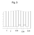
- a surface of a solar cell 1 having an electrode finger pattern that differs from the pattern in FIG Fig. 2 differs by another encoding electrode finger 35.
- the further encoding electrode finger 35 represents another digit of the number in the rank system.
- the corresponding electrode finger 3 in the Fig. 2 may also be considered as a coding electrode finger 35, but which represents the digit 0 in the rank system. If the place value system is a binary system, then it is the in Fig. 3 shown electrode finger pattern to the representation of the decimal number 3.
- a non-coding electrode finger 33 is located between the two coding electrode fingers 35 each representing 1 bit.
- This intermediate finger serves as a spacer between the coding electrode fingers 35 in order to ensure reliable and simple readout. If this intermediate finger were missing, there would be a risk that the two in the Fig. 3 shown encoding electrode fingers 35 as a single encoding electrode finger 35 would be interpreted.
- the longer finger connecting the non-coding electrode fingers 33 and the non-coding electrode finger 33 itself can ensure good current drainage at the edge of the solar cell 1.
- a label is first selected with which the solar cell is to be marked.
- This tag which may include a series of alphanumeric characters, including punctuation or other characters represented by an ASCII code, is then coded into a number in a rank system by encoding. In the place value system, the number includes several digits. Each of these numbers is represented by at least one coding electrode finger 35 in the electrode finger pattern to be subsequently produced.
- the value of the digit in the rank system is represented by the distance of an associated encoding electrode finger 35 from an imaginary line connecting the non-coding electrode fingers 35 or the distance of the encoding electrode finger 35 from the edge 7 of the solar cell 1.
- the thus formed staggered electrode-encoding finger 35 may further fulfill its function of collecting and / or relaying currents generated in the solar cell 1. Marking efficiency reduction is minimal or absent.
Landscapes
- Photovoltaic Devices (AREA)
Applications Claiming Priority (1)
| Application Number | Priority Date | Filing Date | Title |
|---|---|---|---|
| DE102008043750A DE102008043750A1 (de) | 2008-11-14 | 2008-11-14 | Verfahren zur Makierung/Codierung einer Solarzelle und Solarzelle |
Publications (2)
| Publication Number | Publication Date |
|---|---|
| EP2187452A2 true EP2187452A2 (fr) | 2010-05-19 |
| EP2187452A3 EP2187452A3 (fr) | 2010-10-20 |
Family
ID=42077117
Family Applications (1)
| Application Number | Title | Priority Date | Filing Date |
|---|---|---|---|
| EP09174084A Withdrawn EP2187452A3 (fr) | 2008-11-14 | 2009-10-26 | Procédé de marquage/codage d'une cellule solaire et cellule solaire |
Country Status (2)
| Country | Link |
|---|---|
| EP (1) | EP2187452A3 (fr) |
| DE (1) | DE102008043750A1 (fr) |
Cited By (4)
| Publication number | Priority date | Publication date | Assignee | Title |
|---|---|---|---|---|
| WO2011154033A3 (fr) * | 2010-06-07 | 2012-03-08 | Q-Cells Se | Procédé pour marquer une cellule solaire et cellule solaire |
| ITUD20110090A1 (it) * | 2011-06-14 | 2012-12-15 | Applied Materials Italia Srl | Cella fotovoltaica provvista di un codice identificativo e procedimento per realizzarla |
| WO2015012008A1 (fr) * | 2013-07-25 | 2015-01-29 | シャープ株式会社 | Photopile de type électrode arrière, module de photopile faisant appel à une photopile de type électrode arrière et procédé de fabrication de photopile de type électrode arrière |
| CN113410237A (zh) * | 2020-03-17 | 2021-09-17 | 铠侠股份有限公司 | 半导体存储装置 |
Families Citing this family (1)
| Publication number | Priority date | Publication date | Assignee | Title |
|---|---|---|---|---|
| DE102010032469B4 (de) * | 2010-07-28 | 2014-12-04 | Ioss Intelligente Optische Sensoren & Systeme Gmbh | Verfahren und Vorrichtung zum Lesen von Codes auf Solarzellen-Wafern |
Family Cites Families (6)
| Publication number | Priority date | Publication date | Assignee | Title |
|---|---|---|---|---|
| JPH0677509A (ja) * | 1992-08-25 | 1994-03-18 | Sanyo Electric Co Ltd | 太陽電池に於けるセル識別方式 |
| EP1868249B1 (fr) * | 1999-09-28 | 2011-07-13 | Kaneka Corporation | Procédé de contrôle du processus de fabrication d'un appareil de conversion photoélectrique |
| JP2002064214A (ja) * | 2000-08-17 | 2002-02-28 | Honda Motor Co Ltd | 太陽電池の集電用電極およびその製造方法 |
| JP2004259790A (ja) * | 2003-02-25 | 2004-09-16 | Canon Inc | マークを付与した基板の製造方法及びマークの読み取りプログラム及びマークの読み取り装置 |
| EP1989740B2 (fr) * | 2006-02-28 | 2019-05-22 | Hanwha Q CELLS GmbH | Procede de marquage de cellules solaires et cellules solaires |
| US7804022B2 (en) * | 2007-03-16 | 2010-09-28 | Sunpower Corporation | Solar cell contact fingers and solder pad arrangement for enhanced efficiency |
-
2008
- 2008-11-14 DE DE102008043750A patent/DE102008043750A1/de not_active Ceased
-
2009
- 2009-10-26 EP EP09174084A patent/EP2187452A3/fr not_active Withdrawn
Cited By (6)
| Publication number | Priority date | Publication date | Assignee | Title |
|---|---|---|---|---|
| WO2011154033A3 (fr) * | 2010-06-07 | 2012-03-08 | Q-Cells Se | Procédé pour marquer une cellule solaire et cellule solaire |
| ITUD20110090A1 (it) * | 2011-06-14 | 2012-12-15 | Applied Materials Italia Srl | Cella fotovoltaica provvista di un codice identificativo e procedimento per realizzarla |
| WO2015012008A1 (fr) * | 2013-07-25 | 2015-01-29 | シャープ株式会社 | Photopile de type électrode arrière, module de photopile faisant appel à une photopile de type électrode arrière et procédé de fabrication de photopile de type électrode arrière |
| JP2015026665A (ja) * | 2013-07-25 | 2015-02-05 | シャープ株式会社 | 裏面電極型太陽電池、裏面電極型太陽電池を使用した太陽電池モジュールおよび裏面電極型太陽電池の製造方法 |
| CN113410237A (zh) * | 2020-03-17 | 2021-09-17 | 铠侠股份有限公司 | 半导体存储装置 |
| CN113410237B (zh) * | 2020-03-17 | 2024-02-02 | 铠侠股份有限公司 | 半导体存储装置 |
Also Published As
| Publication number | Publication date |
|---|---|
| DE102008043750A1 (de) | 2010-05-20 |
| EP2187452A3 (fr) | 2010-10-20 |
Similar Documents
| Publication | Publication Date | Title |
|---|---|---|
| DE69619147T2 (de) | Streifenkodekodierungssystem mit Vierzustandskoden | |
| EP3208100B1 (fr) | Élément de sécurité à codage magnétique et son procédé de fabrication | |
| EP2187452A2 (fr) | Procédé de marquage/codage d'une cellule solaire et cellule solaire | |
| DE2726746B2 (de) | Verfahren und Einrichtung zur Fehlerkontrolle des Oberflächenmusters eines Objektes | |
| DE3512708C1 (de) | Optoelektronische Messlatte | |
| DE3330261A1 (de) | Verfahren zum codieren bzw. dekodieren von informationen, vorrichtung zum aufbringen der codierten information auf eine druckform bzw. zum uebertragen der information von der druckform auf einen anderen informationstraeger und die druckform selbst | |
| CH616254A5 (fr) | ||
| DE102018008539A1 (de) | Kalibriervorrichtung und Verfahren zur Kamerakalibrierung für die Photogrammetrie | |
| DE102018204259A1 (de) | Verfahren zum Herstellen eines mit einem Code versehenen Bauteils sowie Bauteil mit einem Code | |
| DE102013220747A1 (de) | Maßverkörperung für ein absolutes Positionsmesssystem | |
| DE102015118836B4 (de) | Optisch lesbarer Code und Verfahren zur Kennzeichnung von Leiterplatten mittels eines optisch lesbaren Codes | |
| DE2823679C2 (fr) | ||
| DE102017118509B4 (de) | Zylinder mit einer Kolbenstange und einem optischen Positionsmesser | |
| DE102009009499B4 (de) | Markierungsverfahren, Halbleiterbauelement sowie Solar-Modul | |
| DE2817630A1 (de) | Verfahren zum beurteilen der eingelesenen daten fuer einen etikettenleser | |
| DE2756832A1 (de) | Addierer fuer fibonacci-codes | |
| DE2746779A1 (de) | Taktgebevorrichtung bei einem ausweiskarten-lesegeraet | |
| DE102023120909B3 (de) | Elektronisches Bauelement zum Messen eines elektrischen Stroms, Leiterplatte sowie Messanordnung | |
| DE102008001876A1 (de) | Sensoranordnung und Verfahren zum Betrieb einer Sensoranordnung | |
| DE102011003284A1 (de) | Leistungshalbleiterelement und Anordnung eines Leistungshalbleiterelements zu mindestens einer Solarzelle | |
| DE102018112398A1 (de) | Vorrichtung zur Erfassung einer linearen Verschiebung | |
| DE102023107507A1 (de) | Verfahren zur Bereitstellung eines SMD-Bauelements und entsprechendes SMD-Bauelement | |
| EP0365702A1 (fr) | Transmetteur de position numérique | |
| DE202021100822U1 (de) | Solarzellenmodul und Solarzellenmodulsystem | |
| DE102023134831A1 (de) | Greifelement zum Einsatz in der Robotik und Kobotik |
Legal Events
| Date | Code | Title | Description |
|---|---|---|---|
| PUAI | Public reference made under article 153(3) epc to a published international application that has entered the european phase |
Free format text: ORIGINAL CODE: 0009012 |
|
| AK | Designated contracting states |
Kind code of ref document: A2 Designated state(s): AT BE BG CH CY CZ DE DK EE ES FI FR GB GR HR HU IE IS IT LI LT LU LV MC MK MT NL NO PL PT RO SE SI SK SM TR |
|
| AX | Request for extension of the european patent |
Extension state: AL BA RS |
|
| PUAL | Search report despatched |
Free format text: ORIGINAL CODE: 0009013 |
|
| RAP1 | Party data changed (applicant data changed or rights of an application transferred) |
Owner name: Q-CELLS SE |
|
| AK | Designated contracting states |
Kind code of ref document: A3 Designated state(s): AT BE BG CH CY CZ DE DK EE ES FI FR GB GR HR HU IE IS IT LI LT LU LV MC MK MT NL NO PL PT RO SE SI SK SM TR |
|
| AX | Request for extension of the european patent |
Extension state: AL BA RS |
|
| STAA | Information on the status of an ep patent application or granted ep patent |
Free format text: STATUS: THE APPLICATION IS DEEMED TO BE WITHDRAWN |
|
| 18D | Application deemed to be withdrawn |
Effective date: 20110421 |