EP2187720A1 - Flexible leiterplatte und herstellungsverfahren dafür - Google Patents
Flexible leiterplatte und herstellungsverfahren dafür Download PDFInfo
- Publication number
- EP2187720A1 EP2187720A1 EP08873265A EP08873265A EP2187720A1 EP 2187720 A1 EP2187720 A1 EP 2187720A1 EP 08873265 A EP08873265 A EP 08873265A EP 08873265 A EP08873265 A EP 08873265A EP 2187720 A1 EP2187720 A1 EP 2187720A1
- Authority
- EP
- European Patent Office
- Prior art keywords
- base material
- flexible
- flexible base
- layer
- insulation layers
- Prior art date
- Legal status (The legal status is an assumption and is not a legal conclusion. Google has not performed a legal analysis and makes no representation as to the accuracy of the status listed.)
- Withdrawn
Links
Images


Classifications
-
- H—ELECTRICITY
- H05—ELECTRIC TECHNIQUES NOT OTHERWISE PROVIDED FOR
- H05K—PRINTED CIRCUITS; CASINGS OR CONSTRUCTIONAL DETAILS OF ELECTRIC APPARATUS; MANUFACTURE OF ASSEMBLAGES OF ELECTRICAL COMPONENTS
- H05K3/00—Apparatus or processes for manufacturing printed circuits
- H05K3/46—Manufacturing multilayer circuits
- H05K3/4688—Composite multilayer circuits, i.e. comprising insulating layers having different properties
- H05K3/4691—Rigid-flexible multilayer circuits comprising rigid and flexible layers, e.g. having in the bending regions only flexible layers
-
- H—ELECTRICITY
- H05—ELECTRIC TECHNIQUES NOT OTHERWISE PROVIDED FOR
- H05K—PRINTED CIRCUITS; CASINGS OR CONSTRUCTIONAL DETAILS OF ELECTRIC APPARATUS; MANUFACTURE OF ASSEMBLAGES OF ELECTRICAL COMPONENTS
- H05K3/00—Apparatus or processes for manufacturing printed circuits
- H05K3/46—Manufacturing multilayer circuits
-
- H—ELECTRICITY
- H05—ELECTRIC TECHNIQUES NOT OTHERWISE PROVIDED FOR
- H05K—PRINTED CIRCUITS; CASINGS OR CONSTRUCTIONAL DETAILS OF ELECTRIC APPARATUS; MANUFACTURE OF ASSEMBLAGES OF ELECTRICAL COMPONENTS
- H05K1/00—Printed circuits
- H05K1/02—Details
-
- H—ELECTRICITY
- H05—ELECTRIC TECHNIQUES NOT OTHERWISE PROVIDED FOR
- H05K—PRINTED CIRCUITS; CASINGS OR CONSTRUCTIONAL DETAILS OF ELECTRIC APPARATUS; MANUFACTURE OF ASSEMBLAGES OF ELECTRICAL COMPONENTS
- H05K1/00—Printed circuits
- H05K1/02—Details
- H05K1/0213—Electrical arrangements not otherwise provided for
- H05K1/0216—Reduction of cross-talk, noise or electromagnetic interference
- H05K1/0218—Reduction of cross-talk, noise or electromagnetic interference by printed shielding conductors, ground planes or power plane
-
- H—ELECTRICITY
- H05—ELECTRIC TECHNIQUES NOT OTHERWISE PROVIDED FOR
- H05K—PRINTED CIRCUITS; CASINGS OR CONSTRUCTIONAL DETAILS OF ELECTRIC APPARATUS; MANUFACTURE OF ASSEMBLAGES OF ELECTRICAL COMPONENTS
- H05K2201/00—Indexing scheme relating to printed circuits covered by H05K1/00
- H05K2201/01—Dielectrics
- H05K2201/0183—Dielectric layers
- H05K2201/0187—Dielectric layers with regions of different dielectrics in the same layer, e.g. in a printed capacitor for locally changing the dielectric properties
-
- H—ELECTRICITY
- H05—ELECTRIC TECHNIQUES NOT OTHERWISE PROVIDED FOR
- H05K—PRINTED CIRCUITS; CASINGS OR CONSTRUCTIONAL DETAILS OF ELECTRIC APPARATUS; MANUFACTURE OF ASSEMBLAGES OF ELECTRICAL COMPONENTS
- H05K2201/00—Indexing scheme relating to printed circuits covered by H05K1/00
- H05K2201/07—Electric details
- H05K2201/0707—Shielding
- H05K2201/0715—Shielding provided by an outer layer of PCB
-
- H—ELECTRICITY
- H05—ELECTRIC TECHNIQUES NOT OTHERWISE PROVIDED FOR
- H05K—PRINTED CIRCUITS; CASINGS OR CONSTRUCTIONAL DETAILS OF ELECTRIC APPARATUS; MANUFACTURE OF ASSEMBLAGES OF ELECTRICAL COMPONENTS
- H05K2201/00—Indexing scheme relating to printed circuits covered by H05K1/00
- H05K2201/09—Shape and layout
- H05K2201/09009—Substrate related
- H05K2201/09127—PCB or component having an integral separable or breakable part
-
- H—ELECTRICITY
- H05—ELECTRIC TECHNIQUES NOT OTHERWISE PROVIDED FOR
- H05K—PRINTED CIRCUITS; CASINGS OR CONSTRUCTIONAL DETAILS OF ELECTRIC APPARATUS; MANUFACTURE OF ASSEMBLAGES OF ELECTRICAL COMPONENTS
- H05K2201/00—Indexing scheme relating to printed circuits covered by H05K1/00
- H05K2201/09—Shape and layout
- H05K2201/09209—Shape and layout details of conductors
- H05K2201/095—Conductive through-holes or vias
- H05K2201/09509—Blind vias, i.e. vias having one side closed
-
- H—ELECTRICITY
- H05—ELECTRIC TECHNIQUES NOT OTHERWISE PROVIDED FOR
- H05K—PRINTED CIRCUITS; CASINGS OR CONSTRUCTIONAL DETAILS OF ELECTRIC APPARATUS; MANUFACTURE OF ASSEMBLAGES OF ELECTRICAL COMPONENTS
- H05K2201/00—Indexing scheme relating to printed circuits covered by H05K1/00
- H05K2201/09—Shape and layout
- H05K2201/09209—Shape and layout details of conductors
- H05K2201/095—Conductive through-holes or vias
- H05K2201/09563—Metal filled via
-
- H—ELECTRICITY
- H05—ELECTRIC TECHNIQUES NOT OTHERWISE PROVIDED FOR
- H05K—PRINTED CIRCUITS; CASINGS OR CONSTRUCTIONAL DETAILS OF ELECTRIC APPARATUS; MANUFACTURE OF ASSEMBLAGES OF ELECTRICAL COMPONENTS
- H05K3/00—Apparatus or processes for manufacturing printed circuits
- H05K3/46—Manufacturing multilayer circuits
- H05K3/4602—Manufacturing multilayer circuits characterized by a special circuit board as base or central core whereon additional circuit layers are built or additional circuit boards are laminated
-
- H—ELECTRICITY
- H05—ELECTRIC TECHNIQUES NOT OTHERWISE PROVIDED FOR
- H05K—PRINTED CIRCUITS; CASINGS OR CONSTRUCTIONAL DETAILS OF ELECTRIC APPARATUS; MANUFACTURE OF ASSEMBLAGES OF ELECTRICAL COMPONENTS
- H05K3/00—Apparatus or processes for manufacturing printed circuits
- H05K3/46—Manufacturing multilayer circuits
- H05K3/4644—Manufacturing multilayer circuits by building the multilayer layer by layer, i.e. build-up multilayer circuits
- H05K3/4652—Adding a circuit layer by laminating a metal foil or a preformed metal foil pattern
-
- Y—GENERAL TAGGING OF NEW TECHNOLOGICAL DEVELOPMENTS; GENERAL TAGGING OF CROSS-SECTIONAL TECHNOLOGIES SPANNING OVER SEVERAL SECTIONS OF THE IPC; TECHNICAL SUBJECTS COVERED BY FORMER USPC CROSS-REFERENCE ART COLLECTIONS [XRACs] AND DIGESTS
- Y10—TECHNICAL SUBJECTS COVERED BY FORMER USPC
- Y10T—TECHNICAL SUBJECTS COVERED BY FORMER US CLASSIFICATION
- Y10T29/00—Metal working
- Y10T29/49—Method of mechanical manufacture
- Y10T29/49002—Electrical device making
- Y10T29/49117—Conductor or circuit manufacturing
- Y10T29/49124—On flat or curved insulated base, e.g., printed circuit, etc.
- Y10T29/49155—Manufacturing circuit on or in base
Definitions
- the present invention relates to a bendable flexible wiring board and its manufacturing method.
- Patent Literature 1 to 3 As for a wiring board, part of which is rigid and the other part flexible, for example, some are disclosed in Patent Literature 1 to 3.
- the present invention was carried out considering the above situation.
- the objective is to provide a flexible wiring board with high reliability, especially high connection reliability, and its manufacturing method.
- another objective of the present invention is to provide a flexible wiring board which is easy to manufacture at low cost, and its manufacturing method.
- first flexible base material and second flexible base material are formed with different materials, and the first flexible base material is formed with a material having more flexibility and higher abrasion and heat resistance than the second flexible base material.
- the second flexible base material is formed by laminating multiple flexible sheets.
- first flexible sheet and second flexible sheet are disposed so as to sandwich a tip of first flexible base material.
- the first flexible sheet and second flexible sheet may be configured to correspond to the outline of first flexible base material.
- first and second insulation layers are preferred to be configured to correspond to the outline of the tip of first flexible base material and that of the second flexible base material.
- conductive patterns are formed on the surfaces of the second flexible base material.
- insulation layers cover the border region between the tip of first flexible base material and the edge of second flexible base material.
- vias are formed in insulation layers, and conductive patterns on the insulation layers are connected to conductive patterns in the first flexible base material through the vias.
- upper-layer insulation layers are further formed.
- upper-layer conductive patterns are formed on the upper-layer insulation layers, and conductive patterns on the insulation layers and the upper-layer conductive patterns are connected through upper-layer vias filled with plated metal.
- first upper-layer insulation layers are further formed; on the first upper-layer insulation layers, first upper-layer conductive patterns are formed; on the first upper-layer conductive patterns, second upper-layer insulation layers are formed; on the second upper-layer insulation layers, second upper-layer conductive patterns are formed; the conductive patterns on the insulation layers and the first upper-layer conductive patterns are connected through first upper-layer vias filled with plated metal; and substantially directly on top of the first upper-layer vias in the second upper-layer insulation layers, second upper-layer vias are formed that connect the first upper-layer conductive patterns and the second upper-layer conductive patterns and are filled with plated metal.
- upper-layer insulation layers are formed; on the upper-layer insulation layers, upper-layer vias are formed that are connected to the conductive patterns on the insulation layers; and on the upper-layer insulation layers, conductive patterns connected to the upper-layer vias are formed.
- first flexible base material and second flexible base material be formed with different materials, and that the first flexible base material be formed with a material having higher flexibility and higher abrasion and heat resistance than the second flexible base material.
- the first flexible base material By forming the first flexible base material with a material having high flexibility and high abrasion resistance, its durability when the exposed portion of the first flexible base material is bent may be enhanced. By forming the first flexible base material with a material having high thermal resistance, the base material will not be damaged by heat during the reflow process for soldering when mounting an electronic component in the first flexible base material. Thus, the electronic component may be mounted.
- the second flexible base material may be formed by laminating multiple flexible sheets.
- first flexible sheet and second flexible sheet are disposed so as to sandwich a tip of first flexible base material.
- first flexible sheet and second flexible sheet are configured to correspond to the outline of the first flexible base material.
- first and second insulation layers may be configured to correspond to the outline of the tip of the first flexible base material and that of the second flexible base material.
- upper-layer insulation layers are formed; on the upper-layer insulation layers, upper-layer conductive patterns are formed; and conductive patterns on the insulation layers and upper-layer conductive patterns are connected through upper-layer vias formed in the upper-layer insulation layers and filled with plated metal.
- vias are filled with metal.
- the vias penetrate the insulation layers and are filled with plated metal; on the insulation layers, upper-layer insulation layers and upper-layer conductive patterns are laminated; in the upper-layer insulation layers, upper-layer vias are formed that connect the conductive patterns formed on the insulation layers and the upper-layer conductive patterns; and the upper-layer vias are connected to the vias filled with the plated metal.
- conductive patterns on the insulation layers are extended to the edges of the insulation layers.
- Plane conductive layers may be formed on the edge of the insulation layers positioned on the side of the first flexible base material.
- the first flexible base material has multiple connection pads which are connected to vias, and the pitch of the connection pads is wider than the pitches of the multiple conductive patterns formed in the first flexible base material.
- the conductive patterns are formed in such a way that their pitches widen toward the connection pads and are electrically connected to corresponding connection pads.
- upper-layer insulation layers are formed; on the upper-layer insulation layers, upper-layer conductive patterns are formed; the conductive patterns on the insulation layers and the upper-layer conductive patterns are connected through the upper-layer vias formed in the upper-layer insulation layers; and the edges of the insulation layers on the side of the first flexible base material protrude beyond the edges of the upper-layer insulation layers on the side of the first flexible base material.
- upper-layer insulation layers are formed; on the upper-layer insulation layers, upper-layer conductive patterns are formed; the conductive patterns on the insulation layers and the upper-layer conductive patterns are connected through the upper-layer vias formed in the upper-layer insulation layers; and in the upper-layer vias, cured conductive paste is filled.
- a flexible wiring board of a third aspect of the present invention comprises:
- the vias formed in the insulation layers penetrate the protective layers.
- the conductive patterns formed on the insulation layers and the conductive patterns in the first flexible base material are connected.
- the first flexible base material and the second flexible base material are formed with different materials, and the first flexible base material is formed with a material having more flexibility and higher abrasion and heat resistance than the second flexible base material.
- the second flexible base material is formed by laminating multiple flexible sheets.
- the second flexible base material is formed by laminating multiple flexible sheets; and the first flexible sheet and second flexible sheet are disposed so as to sandwich the tip of first flexible base material.
- the second flexible base material is formed by laminating multiple flexible sheets; first flexible sheet and second flexible sheet are disposed so as to sandwich the tip of first flexible base material; the first flexible base material has different levels at the tip; and first flexible sheet and second flexible sheet are configured to correspond to the outline of the first flexible base material.
- the first flexible base material has different levels at the tip, and the first and second insulation layers are configured to correspond to the outline of the tip of the first flexible base material and that of the second flexible base material.
- the width of the section where the first flexible base material and the insulation layers are stacked is wider than the width where they are not stacked.
- the width of the border between the first flexible base material and the insulation layers is wider than the rest.
- the protective layer includes an insulative film.
- vias are formed that penetrate them and electrically connect the conductive patterns on the insulation layers and the conductive patterns formed in the first flexible base material.
- the protective layer in the first flexible base material includes, for example, an electromagnetic shield layer.
- a conductive pattern is formed, an insulative film is formed on the conductive pattern and an electromagnetic shield layer is formed on the insulative film.
- a conductive pattern is formed; on the conductive pattern, an insulative film is formed; on the insulative film, an electromagnetic shield layer is formed; and on the electromagnetic shield layer, a protective layer is formed.
- a conductive pattern is formed; on the conductive pattern, an insulative film is formed; on the insulative film, an electromagnetic shield layer is formed; and on the electromagnetic shield layer, a protective layer which is in contact with the insulation layer is formed.
- a method of manufacturing a flexible wiring board according to a fourth aspect of the present invention comprises:
- First flexible base material and second flexible base material are formed with different materials.
- the first flexible base material is formed with a material having higher flexibility and higher abrasion and heat resistance than the second flexible base material.
- the first flexible base material is made of, for example, polyimide, liquid crystal polymer or polyether ether ketone.
- the second flexible base material is made of, for example, polyester or glass-epoxy material (the thickness of the board is 0.2 mm or less).
- the interior of the via is filled with plated metal.
- both the top and bottom sides of the border between the flexible base material and the non-flexible base material are covered.
- the above flexible wiring board may be manufactured, for example, by preparing a first flexible base material having a conductive pattern and a second flexible base material having a conductive pattern; disposing the first and second flexible base materials adjacent to each other; disposing insulation layers on the border region between the first and second flexible base materials; further disposing conductive layers on the insulation layers; pressing them; forming vias that penetrate the insulation layers and reach the conductive layers; plating the resultant structure to form plated layers on the surfaces and vias; and patterning the plated layers.
- the following may be conducted: on the patterned plated layers, disposing second insulation layers; in the second insulation layers, forming vias that reach the conductive layers on the insulation layers; plating the resultant structure to form plated layers on its surfaces and vias; and patterning the plated layers.
- the conductor on the first flexible base material may be removed.
- the present invention enables provision of a flexible wiring board with high reliability, especially high connection reliability and its manufacturing method. Also, a flexible wiring board which is easy to manufacture at low cost and its manufacturing method are provided.
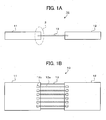
- Flexible wiring board (10) is, as shown in FIGS. 1A and 1B , structured with first multilayer substrate (11), second multilayer substrate (12) and flexible substrate (13) connecting the first and second multilayer substrates (11, 12).
- First and second multilayer substrates (11, 12) are flexible and may be bent to a certain degree.
- any circuit patterns are formed to which, according to requirements, electronic components such as a semiconductor chip or the like are connected.
- Flexible substrate (13) is flexible and may be bent at any point.
- striped wiring (13a) is formed to connect the circuit patterns on first multilayer substrate (11) and second multilayer substrate (12). At both ends of wiring (13a), connection pads (13b) are placed. To connection pads (13b), land portions of the circuit patterns on multilayer substrates (11, 12) are connected. The circuit patterns on first and second multilayer substrates (11, 12) are connected to each other by means of wiring (13a).
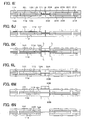
- FIG. 2 is an enlarged cross-sectional view of the area indicated as "2" in FIG. 1A .
- flexible substrate (13) is formed by laminating first flexible base material (131), conductive layers (132, 133), insulation layers (134, 135), shield layers (136, 137) and coverlays (138, 139).
- First flexible base material (131) is formed with an insulative flexible sheet, for example, a polyimide sheet, polyester sheet, liquid crystal polymer sheet or polyether-ether-ketone sheet, with a thickness in the range of 20-50 ⁇ m, preferably with a thickness of approximately 30 ⁇ m.
- an insulative flexible sheet for example, a polyimide sheet, polyester sheet, liquid crystal polymer sheet or polyether-ether-ketone sheet, with a thickness in the range of 20-50 ⁇ m, preferably with a thickness of approximately 30 ⁇ m.
- Conductive layers (132, 133) are formed respectively on the top and bottom surfaces of first flexible base material (131), structuring striped wiring (13a) as shown in FIG. 1B .
- Conductive layers (132, 133) are formed, for example, from copper patterns with a thickness of approximately 5-15 ⁇ m.
- Insulation layers (134, 135) are formed with an approximately 5-15 ⁇ m-thick insulative film such as polyimide film, polyester film, liquid-crystal polymer film or polyether-ether film, which insulate conductive layers (132, 133) from the outside.
- insulative film such as polyimide film, polyester film, liquid-crystal polymer film or polyether-ether film, which insulate conductive layers (132, 133) from the outside.
- Shield layers (136, 137) are formed with conductive layers, for example, cured silver-paste films, and they shield conductive layers (132, 133) from outside electromagnetic noise as well as shield electromagnetic noise from conductive layers (132, 133) to the outside.
- Coverlays (138, 139) are formed with, for example, an approximately 5-15 ⁇ m-thick insulative film such as polyimide, and they insulate the entire flexible substrate (13) from the outside and protect it as well.
- first multilayer substrate (11) is formed by laminating second flexible base material (101), first and second insulation layers (112, 113) and first and second upper-layer insulation layers (114, 115).
- Second flexible base material (101) provides strength for multilayer substrate (11) and is formed with, for example, a material having excellent insulation and flexibility which costs less than polyimide, such as heat-resistant polyester or the like. Second flexible base material (101) is disposed horizontal to, but separated from, first flexible base material (131) of flexible substrate (13).
- circuit patterns (103, 105) are formed on both surfaces of second flexible base material (101). Circuit patterns (103, 105) are connected to each other according to requirements through filled vias (107) or the like that are filled with conductor such as copper. Furthermore, circuit patterns (103, 104) are connected to other circuits through vias or wiring not shown in the drawing.
- First and second insulation layers (112, 113) are formed with insulative base material such as polyimide, polyester, liquid crystal polymer or polyether ether and are joined by an adhesive agent to flexible substrate (13) and second flexible base material (101).
- First and second insulation layers (112, 113) each have a thickness in the range of 50-100 ⁇ m, preferably approximately 50 ⁇ m.
- First and second insulation layers (112, 113) cover second flexible base material (101) and the tip of flexible substrate (13) on both the top and bottom surfaces, and expose part of flexible substrate (13).
- Second flexible base material (101) and first and second insulation layers (112, 113) form the flexible core of multilayer substrate (11), and support and anchor flexible substrate (13) by sandwiching its tip.
- vias via holes or contact holes
- shield layer (137) and coverlay (139) are removed from the portion facing vias (116) (the portion where connection pads (13b) of wiring (13a) are formed). Vias (116) penetrate second insulation layer (113) and insulation layer (135) in flexible substrate (13), and expose connection pads (13b) of conductive layer (133).
- via (116) On the inner surface of via (116), conductive layer (117) made of plated copper or the like is formed. Conductive layers (117) are connected through plating to connection pads (13b) of conductive layer (133) in flexible substrate (13). Also, vias (116) have a conformal via structure.
- Extended pattern (118) is formed from a copper-plated layer or the like.
- copper pattern (124) insulated from the rest is disposed at an edge of second insulation layer (113), namely at the section positioned beyond the border between flexible substrate (13) and second flexible base material (101). Copper pattern (124) works as a radiation board. Thus, the heat generated in multilayer substrate (11) may be effectively radiated.
- First upper-layer insulation layer (114) is laminated on second insulation layer (113).
- First upper-layer insulation layer (114) is formed with a flexible insulative film such as polyimide, polyester, liquid crystal polymer or polyether ether ketone, and is adhered to second insulation layer (113).
- first upper-layer insulation layer (114) may be formed by curing a prepreg made by impregnating resin in glass cloth or the like. However, because the prepreg itself is very thin, first upper-layer insulation layer (114) also has a certain degree of flexibility.
- first upper-layer insulation layer (114) On first upper-layer insulation layer (114), second upper-layer insulation layer (115) is disposed. Second upper-layer insulation layer (115) is formed with a flexible insulative film such as polyimide, polyester, liquid crystal polymer or polyether ether ketone, and is adhered to second insulation layer (113). Alternatively, first upper-layer insulation layer (114) may be formed by curing a prepreg made by impregnating resin in glass cloth or the like.
- first upper-layer insulation layer (114) vias (first upper-layer vias) (119) connected to extended pattern (118) are formed. Vias (119) are filled with conductor (120) such as copper. Also, on second upper-layer insulation layer (115) laminated on first upper-layer insulation layer (114), vias (second upper-layer vias) (121) connected to vias (119) are formed. Vias (121) are filled with conductor (120) such as copper. Namely, filled built-up vias are formed with vias (119, 121).
- conductive pattern (circuit pattern) (123) is formed appropriately. Vias (119) are also connected appropriately to conductive pattern (123).
- multilayer substrate (12), and that of the joint section between multilayer substrate (12) and flexible substrate (13) are the same as the structure of multilayer substrate (11) shown in FIG. 1 and that of the joint section between multilayer substrate (11) and flexible substrate (13).
- the tip of flexible substrate (13) is inserted between first and second insulation layer (112, 113) that form the core section of multilayer substrate (11). Furthermore, by means of conductive layers (copper-plated layers) (117) formed in vias (116) which are formed in second insulation layer (113) and insulation layer (135), connection pads (13b) of conductive layer (133) in flexible substrate (13) and conductive pattern (123) on multilayer substrate (11) are connected.
- conductive layer (133) in flexible substrate (13) and conductive layers (117) in vias (116) in multilayer substrate (11) are connected through plating. Thus, the reliability of the joint section is high.
- first and second insulation layers (112, 113) on the side of flexible substrate (13) protrude beyond the edge surface of upper-layer insulation layer (114) on the side of flexible substrate (13). Therefore, when flexible substrate (13) is bent, the stress exerted on flexible substrate (13) is seldom conveyed to the joint section of multilayer substrate (11) (vias 116, conductive layers 117). Accordingly, stress exerted on the joint section between multilayer substrate (11) and flexible substrate (13) is lowered, and thus its reliability is high.
- multilayer substrate (11) is formed in such a way that its core section holds the expansion/shrinkage of flexible substrate (13), which tends to expand/shrink easily, in a horizontal direction. Therefore, reliability against mechanical bending and heat-resistance reliability are high.
- flexible wiring board (10) is structured in such a way that first and second insulation layers (112, 113) of multilayer substrate (11) sandwich the tip of flexible substrate (13).
- first and second insulation layers (112, 113) of multilayer substrate (11) sandwich the tip of flexible substrate (13).
- the margin of error in aligning the connection land (via 116) of multilayer substrate (11) may be minimized.
- the diameter of vias (116) may be designed to be smaller.
- second flexible base material (101) is formed with a material having high flexibility and high abrasion resistance, durability may be enhanced when flexible substrate (13) is bent.
- second flexible base material (101) is formed with material having high heat resistance, it will not be damaged by heat during the reflow process to fuse solder. Accordingly, an electronic component may be mounted.
- the manufacturing cost may be suppressed without lowering the level of performance.
- Conductive layer (132), insulation layer (134), shield layer (136) and coverlay (138) may be removed from the structure of flexible substrate (13) shown in FIG. 2 .
- conductive patterns were formed only on the top surfaces of multilayer substrates (11, 12).
- the present invention is not limited to such an example.
- conductive patterns may also be formed on the bottom surfaces of multilayer substrates (11, 12).
- vias (141) are formed in first insulation layer (112) and insulation layer (134) of flexible substrate (13).
- conductor (142) such as copper is filled and connected to extended pattern (143) formed on first insulation layer (112).
- Third and fourth upper-layer insulation layers (144, 145) are laminated and disposed on first insulation layer (112). Third and fourth upper-layer insulation layers (144, 145) are also formed with flexible base material or prepreg. In third and fourth upper-layer insulation layers (144, 145), vias (146, 147) are formed respectively.
- vias (116) are filled vias which are filled with conductor (117a).
- a copper film is formed on both surfaces of flexible base material (131) formed with polyimide processed to be a predetermined size.
- conductive layers (132, 133), each having wiring (13a) and connection pads (13b), are formed.
- insulation layers (134, 135) made with polyimide or the like are formed on flexible substrate (13) with the structure shown in FIG. 3 is completed.
- silver paste is applied on the area that excludes the tip of flexible substrate (13) where connection pads (13b) are formed.
- shield layers (136, 137) are formed.
- coverlays (138, 139) are arranged to cover shield layers (136, 137) on the top and bottom surfaces.
- second flexible base material (101) is prepared as shown in FIG. 5A .
- a laser is beamed at the via-formation region in second flexible base material (101) to form vias (107) as shown in FIG. 5B .
- circuit patterns (103, 105) are formed as shown in FIG. 5D .
- flexible substrate (13), second flexible base material (101) to form multilayer substrate (11) and flexible base material (201) to form flexible substrate (13) are arranged.
- flexible base materials to make first insulation layer (112) and second insulation layer (113) are disposed.
- flexible substrate (13) flexible base materials (212, 213) are also disposed.
- conductive films (161, 162) such as copper are disposed.
- the pressure-pressing is conducted, for example, using hydropressing equipment under the following conditions: temperature of 200°C, pressure of 40 kgf and pressing time approximately 3 hours.
- each portion is configured to correspond to each other's shape.
- IVHs Interstitial Via Hole
- vias (116, 141) and others to connect conductive layers (132, 133) of flexible substrate (13) and multilayer substrates (11, 12) are also formed.
- vias (116, 141, 163) copper film may be disposed only on the inner surfaces of vias (116, 141, 163) to make them conformed vias.
- first and second insulation layers (112, 113) third and first upper-layer insulation layers (144, 114) are disposed respectively.
- third and first upper-layer insulation layers (244, 214) are also respectively disposed as well.
- Upper-layer insulation layers (144, 114, 244, 214) are formed with an insulative film such as polyimide, polyethylene, liquid crystal polymer, polyether ether ketone or glass epoxy (for example, 0.2 mm thick or less).
- first and third upper-layer insulation films (114, 214, 144, 244) are adhered to second and first insulation layers (113, 112, 213, 212).
- copper foil (301) is pasted on first upper-layer insulation films (114, 214) using an adhesive agent; and copper foil (302) is pasted on third upper-layer insulation films (144, 244) using an adhesive agent.
- a thermal fusion type is used, then heated to fuse their surfaces, on which copper foils (301, 302) may be pasted.
- vias (119, 146, 219, 246) are formed in first and third upper-layer insulation layers (114, 144, 214, 244).
- copper-plated layers (303, 304) are patterned to form wiring and filled vias.
- the process is repeated in which flexible base materials are laminated, via holes are formed, plating is performed and plated layers are patterned.
- laser “L” is beamed at the areas corresponding to the tips of first and second insulation layers (112, 113, 212, 213). Accordingly, as shown in FIG. 6L , structures (305, 306), which are severed from their surroundings, are formed in the center. Laser “L” is beamed to such an extent that it roughly makes a cutting in copper film (171).
- structures (305, 306) are removed. At that time, since copper foil (171) and flexible substrate (13) are not adhered, the exposed portions of copper foil (171) are removed along with structures (305, 306).
- flexible wiring board (10) is completed in which the tips of flexible substrate (13) are inserted between the core portions of multilayer substrates (11, 12) (first and second insulation layers 112, 113), and the lands of multilayer substrates (11, 12) and connection pads of flexible substrate (13) are connected through plating.
- the material, size and number of layers of each of the above-described layers may be freely modified.
- a circuit pattern may be formed at any position and the circuit pattern may also be formed on any layer.
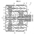
- second flexible base material (101) in multilayer substrates (11, 12) was formed with a layer of flexible sheet.
- it may be formed with multiple flexible sheets.
- second flexible base material (101) is formed with three layers of flexible base material (101a, 101b, 101c).
- Flexible base material (101a) has substantially the same thickness as first flexible base material (131) of flexible substrate (13).
- flexible base material (101b) is adhered to flexible base material (101a), and its edge is configured to correspond to the outline of the different levels formed by coverlay (138) at the tip of flexible substrate (13).
- flexible base material (101c) is adhered to flexible base material (101a), and its tip is configured to correspond to the outline of the different levels formed by coverlay (139) at the tip of flexible substrate (13).
- a tip of flexible substrate (13) (first flexible base material (131), conductive layers (132, 133), insulation layers (134, 135)) is inserted and anchored; furthermore, between second flexible base material (101) (101a-101c) and first and second insulation layers (112, 113), an even longer region of the tip of flexible substrate (13) is inserted and anchored. Accordingly, multilayer substrates (11, 12) may anchor and support flexible substrate (13) even more securely. Thus, the connection reliability between multilayer substrates (11, 12) and flexible substrate (13) is also high.
- a circuit pattern may be formed in each sheet as shown by reference numerals (231-239) in FIG. 8 .
- the material for flexible base materials (101a-101c) may be the same or different.
- flexible base material (101 a) may be formed with polyimide
- flexible base materials (101b, 101c) may be formed with polyester.
- thermopressing flexible substrate (13) and second flexible base material (101) by means of an adhesive agent both are anchored. Furthermore, by disposing the first and second insulation layers, applying an adhesive agent if necessary, and thermopressing them, they will be anchored.
- the first flexible base material to structure flexible substrate (13) may be formed by laminating multiple flexible base materials.
- the material for each flexible base material may be the same or different.
- wiring patterns formed on multilayer substrates (11, 12) and flexible substrate (13) are not limited to the example shown in FIG. 1 , but may be configured, for example, as shown in FIG. 9 , to fan out from flexible substrate (13) toward multilayer substrates (11, 12).
- the pitch of connection pads (13b) may be larger than the pitch of wiring (13a). In doing so, more wiring may be arranged in flexible substrate (13) and a flexible rigid wiring board with high-density wiring may be formed.
- part of flexible substrate (13) may be configured to be wider than the rest as shown in FIGS. 10 and 11 .
- the joint areas between flexible substrate (13) and multilayer substrates (11, 12) increase, thus enhancing the connection reliability of vias.
- the tips of flexible substrate (13) are extended to enlarge the size of the sections anchored by multilayer substrates (11, 12). By doing so, the strength in the tips of flexible substrate (13) increases, thus enhancing their resistance against mechanical bending.
- projected portions are formed where flexible substrate (13) is repeatedly bent (such as the places corresponding to the edge lines of multilayer substrates (11, 12)) to enhance strength in the places which will be repeatedly bent.
- insulation layers were laminated on the flexible base material without an adhesive layer disposed in between. Also, without an adhesive layer, upper-layer insulation layers were laminated on the insulation layers.
- a flexible wiring substrate according to the present invention is not limited to such an embodiment.
- a flexible wiring substrate may be structured as shown in FIG. 12 .
- first insulation layer (112) is laminated beneath flexible base material (101) by means of first adhesive layer (180); and second insulation layer (113) is laminated on flexible base material (101) by means of first adhesive layer (181).
- first upper-layer insulation layer (144) is laminated beneath first insulation layer (112) by means of second adhesive layer (182); and first upper-layer insulation layer (114) is laminated on second insulation layer (113) by means of second adhesive layer (183).
- Second upper-layer insulation layer (145) is laminated beneath first upper-layer insulation layer (144) by means of third adhesive layer (184); also, second upper-layer insulation layer (115) is laminated on first upper-layer insulation layer (114) by means of third adhesive layer (185).
- adhesive layer (186) is formed between insulation layer (135) and flexible base material (101c); and between insulation layer (134) and flexible base material (101b), adhesive layer (187) is formed.
- adhesive layer (188) is formed between flexible base material (101a) and flexible base material (101c); and between flexible base material (101 a) and flexible base material (101b), adhesive layer (189) is formed.
- Flexible base materials are formed with polyimide, polyester or the like.
- first insulation layer (113), second insulation layer (112), first upper-layer insulation layers (114, 144) and second upper-layer insulation layers (115, 145) may also be formed with a resin such as polyimide, polyester or the like.
- Adhesive layers (180, 181, 182, 183, 184, 185, 186, 187, 188, 189) are formed by curing an adhesive agent.
- the adhesive agent is preferred to have a high elasticity ratio, a high glass-transition temperature point and high heat resistance, let alone high adhesiveness. Also, to avoid having a negative impact on the environment, it is preferred to use a halogen-free type.
- thermosetting type epoxy adhesive agent may be used.
- thermal treatment is conducted at temperatures of 100-180°C for a period of several dozen minutes to a few hours.
- the thickness of adhesive layers (180, 181, 182, 183, 184, 185, 186, 187, 188, 189), formed by curing the adhesive agent, may be made in the range of 10-30 ⁇ m.
- the thickness of adhesive layers (180, 181, 182, 183, 184, 185, 186, 187, 188, 189) is made thinner than that of conductive patterns. However, it may be made the same thickness as the conductive patterns, or it may be made thicker than the conductive patterns.
- first adhesive layer (180) With first adhesive layer (180), the adhesiveness between first insulation layer (112) and flexible base material (101) may be enhanced. With first adhesive layer (181), the adhesiveness between second insulation layer (113) and flexible base material (101) may be enhanced.
- second adhesive layer (182) the adhesiveness between first upper-layer insulation layer (144) and first insulation layer (112) may be enhanced.
- second adhesive layer (183) the adhesiveness between first upper-layer insulation layer (114) and second insulation layer (113) may be enhanced.
- third adhesive layer (184) the adhesiveness between second upper-layer insulation layer (145) and first upper-layer insulation layer (144) may be enhanced.
- third adhesive layer (185) the adhesiveness between second upper-layer insulation layer (115) and first upper-layer insulation layer (114) may be enhanced.
- the adhesiveness between insulation layer (135) and flexible base material (101c) may be enhanced.
- adhesive layer (187) the adhesiveness between insulation layer (134) and flexible base material (101b) may be enhanced.
- adhesive layer (188) the adhesiveness between flexible base material (101a) and flexible base material (101c) may be enhanced.
- adhesive layer (189) the adhesiveness between flexible base material (101a) and flexible base material (101b) may be enhanced.
- a method of manufacturing flex-rigid wiring board (10) is not limited to the example described above with reference to FIGS. 6A-6N .
- separator (291) may be placed in space (113a) between second insulation layers (113) and (213) in the step described with reference to FIG. 6A .
- Separator (291) is formed, for example, with a cured prepreg, polyimide film or the like.
- an adhesive agent may be disposed between the separator and copper foil (162).
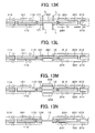
- FIG. 13B Next, the entire structure is pressed as shown in FIG. 13B .
- vias (116, 141, 163) are formed.
- FIG. 13D using conductive film (162) as a seed layer, copper film (171) is formed.
- FIG. 13E copper film (171) is patterned to form copper patterns.
- first insulation layers (112, 212) on first insulation layers (112, 212), second upper-layer insulation layer (prepreg) (144) is disposed. Also, on second insulation layers (113, 213), first upper-layer insulation layer (prepreg) (114) is disposed. Then, they are pressed.
- copper foils (301, 302) are respectively pasted on upper-layer insulation films (114, 144) by means of an adhesive agent.
- a thermal fusion type is used, and then heated to fuse their surfaces, on which copper foil (301, 302) may be pasted. Then, a process such as roughening the surfaces of copper foils (301, 302) is conducted to enhance laser beam reception performance.
- vias (119, 146, 219, 246) are formed in upper-layer insulation layers (114, 144).
- copper-plated layers (303, 304) are patterned to form wiring and filled vias.
- the steps are repeated in which flexible base materials are laminated, via holes are formed, plating is performed and plated layers are patterned.
- laser “L” is beamed from the top and bottom sides of flexible base material (13) to cut off upper-layer insulation layers (114, 144). Accordingly, as shown in FIG. 13L , structures (305, 306) separated from their surroundings are formed in the center. Laser “L” is beamed to such an extent that it roughly makes a cutting in copper film (171).
- structures (305, 306) are removed. At that time, since copper film (171) and flexible base material (13) are not adhered, the exposed portions of copper film (171) are removed along with structures (305, 306).
- flexible wiring board (10) is completed in which the tips of flexible substrate (13) are inserted between the core portions (first and second insulation layers 112, 113) of multilayer substrates (11, 12), and the lands of multilayer substrates (11, 12) and connection pads of the flexible substrate are connected through plating.
- a manufacturing method, for example, shown in FIGS. 14A-14D may also be employed.
- separator (291) is first placed as shown in FIG. 13A , the steps shown in FIGS. 13B-13F are carried out. Then, using a laser or the like, cutting line (292) is formed on the portion above separator (291) in upper-layer insulation layer (114) as shown in FIG. 14A .
- upper-layer insulation layer (115) is disposed and on upper-layer insulation layer (155), upper-layer insulation layer (145) is disposed.
- separator (293) an edge of which is positioned on cutting line (292), is substituted for part of upper-layer insulation layer (115) as shown in FIG. 14B .
- cutting lines (294, 295) are formed in part of an edge of separator (291) and in part of another edge of separator (291).
- structure (296) formed with cutting line (294), separator (291), cutting line (292), separator (293) and cutting line (295) is removed.
- the area that does not contribute to the formation of circuits may be removed and the volume of the wiring board may be decreased.
- the steps of manufacturing multilayer substrate (12) are modified.
- the steps of manufacturing rigid substrate (11) or those of both multilayer substrates (11, 12) may also be modified.
- examples of modification in the steps of manufacturing the upper portion of flexible wiring board (10) were shown.
- the lower portion of flexible wiring board (10) or the entire structure may be manufactured by the modified method.
- the present invention is applicable for a bendable flexible wiring board.
Landscapes
- Engineering & Computer Science (AREA)
- Microelectronics & Electronic Packaging (AREA)
- Manufacturing & Machinery (AREA)
- Structure Of Printed Boards (AREA)
- Production Of Multi-Layered Print Wiring Board (AREA)
- Printing Elements For Providing Electric Connections Between Printed Circuits (AREA)
- Shielding Devices Or Components To Electric Or Magnetic Fields (AREA)
Applications Claiming Priority (2)
| Application Number | Priority Date | Filing Date | Title |
|---|---|---|---|
| US3516908P | 2008-03-10 | 2008-03-10 | |
| PCT/JP2008/069463 WO2009113202A1 (ja) | 2008-03-10 | 2008-10-27 | フレキシブル配線板及びその製造方法 |
Publications (2)
| Publication Number | Publication Date |
|---|---|
| EP2187720A1 true EP2187720A1 (de) | 2010-05-19 |
| EP2187720A4 EP2187720A4 (de) | 2011-11-23 |
Family
ID=41061773
Family Applications (1)
| Application Number | Title | Priority Date | Filing Date |
|---|---|---|---|
| EP08873265A Withdrawn EP2187720A4 (de) | 2008-03-10 | 2008-10-27 | Flexible leiterplatte und herstellungsverfahren dafür |
Country Status (7)
| Country | Link |
|---|---|
| US (2) | US8405999B2 (de) |
| EP (1) | EP2187720A4 (de) |
| JP (1) | JP4971460B2 (de) |
| KR (1) | KR101098072B1 (de) |
| CN (1) | CN101658081B (de) |
| TW (1) | TWI391064B (de) |
| WO (1) | WO2009113202A1 (de) |
Cited By (1)
| Publication number | Priority date | Publication date | Assignee | Title |
|---|---|---|---|---|
| US10034368B2 (en) | 2012-02-21 | 2018-07-24 | Samsung Electro-Mechanics Co., Ltd. | Flying tail type rigid-flexible printed circuit board |
Families Citing this family (39)
| Publication number | Priority date | Publication date | Assignee | Title |
|---|---|---|---|---|
| US8071883B2 (en) | 2006-10-23 | 2011-12-06 | Ibiden Co., Ltd. | Flex-rigid wiring board including flexible substrate and non-flexible substrate and method of manufacturing the same |
| US7982135B2 (en) * | 2006-10-30 | 2011-07-19 | Ibiden Co., Ltd. | Flex-rigid wiring board and method of manufacturing the same |
| EP2187720A4 (de) * | 2008-03-10 | 2011-11-23 | Ibiden Co Ltd | Flexible leiterplatte und herstellungsverfahren dafür |
| JP5295596B2 (ja) * | 2008-03-19 | 2013-09-18 | 新光電気工業株式会社 | 多層配線基板およびその製造方法 |
| JP5202254B2 (ja) * | 2008-11-27 | 2013-06-05 | 株式会社ジャパンディスプレイイースト | 表示装置および表示装置の製造方法 |
| TWI372558B (en) * | 2009-04-08 | 2012-09-11 | Flexible thin image-sensing module with anti-emi function and flexible thin pcb module with anti-emi function | |
| CN102577646B (zh) * | 2009-09-30 | 2015-03-04 | 株式会社村田制作所 | 电路基板及其制造方法 |
| US20110147069A1 (en) * | 2009-12-18 | 2011-06-23 | International Business Machines Corporation | Multi-tiered Circuit Board and Method of Manufacture |
| TW201127228A (en) | 2010-01-22 | 2011-08-01 | Ibiden Co Ltd | Flex-rigid wiring board and method for manufacturing the same |
| TW201127246A (en) | 2010-01-22 | 2011-08-01 | Ibiden Co Ltd | Flex-rigid wiring board and method for manufacturing the same |
| TW201130405A (en) | 2010-02-23 | 2011-09-01 | Ibiden Co Ltd | Flex-rigid wiring board and method for manufacturing the same |
| JP2012079866A (ja) * | 2010-09-30 | 2012-04-19 | Kinko Denshi Kofun Yugenkoshi | フレックスリジッド回路板とその製造方法 |
| KR101241544B1 (ko) * | 2011-06-10 | 2013-03-11 | 엘지이노텍 주식회사 | 인쇄회로기판 및 그의 제조 방법 |
| CN103458605B (zh) * | 2012-05-30 | 2016-12-14 | 欣兴电子股份有限公司 | 软硬复合电路板及其制作方法 |
| US20130341077A1 (en) * | 2012-06-25 | 2013-12-26 | Ibiden Co., Ltd. | Method for repairing disconnection in wiring board, method for manufacturing wiring board, method for forming wiring in wiring board and wiring board |
| KR101482404B1 (ko) * | 2013-05-27 | 2015-01-13 | 삼성전기주식회사 | 리지드 플렉시블 인쇄회로기판 및 그 제조방법 |
| TWI501713B (zh) * | 2013-08-26 | 2015-09-21 | Unimicron Technology Corp | 軟硬板模組以及軟硬板模組的製造方法 |
| US9868536B2 (en) * | 2013-10-30 | 2018-01-16 | Goodrich Corporation | Electrical interconnects for ice protection systems |
| CN104754855B (zh) * | 2013-12-31 | 2018-01-30 | 鹏鼎控股(深圳)股份有限公司 | 柔性电路板及其制作方法 |
| KR20150125424A (ko) * | 2014-04-30 | 2015-11-09 | 삼성전기주식회사 | 강연성 인쇄회로기판 및 강연성 인쇄회로기판의 제조 방법 |
| USD785575S1 (en) * | 2014-05-28 | 2017-05-02 | Sumitomo Electric Industries, Ltd. | Flexible printed wiring board |
| KR20160073766A (ko) * | 2014-12-17 | 2016-06-27 | 삼성전기주식회사 | 연성 인쇄회로기판 및 그 제조 방법 |
| US10993635B1 (en) | 2016-03-22 | 2021-05-04 | Flextronics Ap, Llc | Integrating biosensor to compression shirt textile and interconnect method |
| JP6694763B2 (ja) * | 2016-06-08 | 2020-05-20 | 信越ポリマー株式会社 | 電磁波シールドフィルムおよび電磁波シールドフィルム付きプリント配線板 |
| JP2018032659A (ja) * | 2016-08-22 | 2018-03-01 | イビデン株式会社 | プリント配線板およびプリント配線板の製造方法 |
| CN209949597U (zh) * | 2016-10-24 | 2020-01-14 | 株式会社村田制作所 | 多层基板 |
| JP6700207B2 (ja) * | 2017-02-08 | 2020-05-27 | 矢崎総業株式会社 | 印刷回路の電気接続方法 |
| CN108538799B (zh) * | 2017-03-02 | 2024-02-27 | 弗莱克斯有限公司 | 互连部件和互连组件 |
| USD877099S1 (en) * | 2017-03-15 | 2020-03-03 | Sumitomo Electric Industries, Ltd. | Flexible printed wiring board for a module |
| WO2019000372A1 (zh) | 2017-06-30 | 2019-01-03 | 深圳市汇顶科技股份有限公司 | 生物特征检测装置及电子终端 |
| CN109219332A (zh) * | 2017-07-03 | 2019-01-15 | 信越聚合物株式会社 | 电磁波屏蔽膜及其制造方法、以及带有电磁波屏蔽膜的印刷电路板及其制造方法 |
| KR20190027579A (ko) * | 2017-09-07 | 2019-03-15 | 삼성전기주식회사 | 인쇄회로기판 |
| US11224117B1 (en) | 2018-07-05 | 2022-01-11 | Flex Ltd. | Heat transfer in the printed circuit board of an SMPS by an integrated heat exchanger |
| US10985484B1 (en) | 2018-10-01 | 2021-04-20 | Flex Ltd. | Electronic conductive interconnection for bridging across irregular areas in a textile product |
| US10638616B1 (en) | 2018-10-30 | 2020-04-28 | Taiwan Semiconductor Manufacturing Co., Ltd. | Circuit carrier and manifacturing method thereof |
| JP7297431B2 (ja) * | 2018-12-11 | 2023-06-26 | 株式会社小糸製作所 | 回路基板及び車両用灯具 |
| WO2022215381A1 (ja) | 2021-04-09 | 2022-10-13 | 株式会社村田製作所 | 接続構造およびアンテナモジュール |
| CN115226293B (zh) * | 2021-04-16 | 2025-09-23 | 鹏鼎控股(深圳)股份有限公司 | 可穿戴设备用固定带、制作方法及可穿戴设备 |
| CN113342209B (zh) * | 2021-06-25 | 2023-05-02 | 武汉华星光电技术有限公司 | 一种显示面板及显示装置 |
Family Cites Families (56)
| Publication number | Priority date | Publication date | Assignee | Title |
|---|---|---|---|---|
| US3471348A (en) * | 1968-10-04 | 1969-10-07 | North American Rockwell | Method of making flexible circuit connections to multilayer circuit boards |
| US4099038A (en) * | 1976-12-22 | 1978-07-04 | The United States Of America As Represented By The Secretary Of The Navy | Separable electrical flexible cable assembly for moving stores such as missiles |
| JPS58212120A (ja) | 1982-06-03 | 1983-12-09 | 日本電気株式会社 | 積層セラミツクコンデンサ |
| US4687695A (en) * | 1985-09-27 | 1987-08-18 | Hamby Bill L | Flexible printed circuits and methods of fabricating and forming plated thru-holes therein |
| US4715928A (en) * | 1985-09-27 | 1987-12-29 | Hamby Bill L | Flexible printed circuits and methods of fabricating and forming plated thru-holes therein |
| JPS63109772A (ja) | 1986-10-28 | 1988-05-14 | Nitto Electric Ind Co Ltd | 植物細胞等の培養方法 |
| JPS63293991A (ja) | 1987-05-19 | 1988-11-30 | ビル エル.ハムビ− | フレキシブルプリント回路およびその製造方法 |
| JPH0693534B2 (ja) | 1990-02-26 | 1994-11-16 | 日本アビオニクス株式会社 | フレキシブル・リジッド・プリント配線板 |
| JPH0424846A (ja) * | 1990-05-18 | 1992-01-28 | Fujitsu Ten Ltd | 書換可能メモリの実装確認方法 |
| US5121297A (en) | 1990-12-31 | 1992-06-09 | Compaq Computer Corporation | Flexible printed circuits |
| JPH0590756A (ja) | 1991-09-28 | 1993-04-09 | Ibiden Co Ltd | リジツドフレキ基板の製造方法 |
| GB9125173D0 (en) | 1991-11-27 | 1992-01-29 | Northumbria Circuits Limited | Printed circuit combination and process |
| DE4208610C1 (en) | 1992-03-18 | 1993-05-19 | Fa. Carl Freudenberg, 6940 Weinheim, De | Rigid-flexible PCB with flexible circuit foil mfg. - having flexible PCB in flexible region with fracture lines in rigid outer layers along rigid-flexible transition allowing rigid part to be removed along fracture lines after processing |
| JPH05315758A (ja) * | 1992-05-01 | 1993-11-26 | Nitto Denko Corp | 多層フレキシブル回路基板およびその製法 |
| US5854534A (en) * | 1992-08-05 | 1998-12-29 | Fujitsu Limited | Controlled impedence interposer substrate |
| JP3224889B2 (ja) | 1993-01-13 | 2001-11-05 | イビデン株式会社 | プリント配線板とその製造方法 |
| JPH0794835A (ja) | 1993-09-21 | 1995-04-07 | Nippon Avionics Co Ltd | フレキシブル・リジッド・プリント配線板 |
| JPH09148731A (ja) | 1995-11-17 | 1997-06-06 | Fujitsu Ltd | 配線基板間の接続構造の製造方法 |
| US6350387B2 (en) * | 1997-02-14 | 2002-02-26 | Teledyne Industries, Inc. | Multilayer combined rigid/flex printed circuit board containing flexible soldermask |
| US6226862B1 (en) * | 1998-04-30 | 2001-05-08 | Sheldahl, Inc. | Method for manufacturing printed circuit board assembly |
| KR100855529B1 (ko) | 1998-09-03 | 2008-09-01 | 이비덴 가부시키가이샤 | 다층프린트배선판 및 그 제조방법 |
| TW478306B (en) | 2000-09-22 | 2002-03-01 | Unitech Printed Circuit Board | Manufacturing method of soft and hard combined multi-layer printed circuit board |
| JP2003152309A (ja) | 2001-11-14 | 2003-05-23 | Nippon Mektron Ltd | 両面可撓性回路基板の製造法 |
| AU2003284573A1 (en) | 2002-11-27 | 2004-06-18 | Sumitomo Bakelite Company Limited | Circuit board, multi-layer wiring board, method for making circuit board, and method for making multi-layer wiring board |
| JP2004266236A (ja) | 2003-01-09 | 2004-09-24 | Sony Chem Corp | 基板素片とその基板素片を用いた複合配線板 |
| US7378596B2 (en) * | 2003-04-18 | 2008-05-27 | Ibiden Co., Ltd. | Rigid-flex wiring board |
| JP4408343B2 (ja) * | 2003-04-30 | 2010-02-03 | 日本圧着端子製造株式会社 | 多層プリント配線板の接続構造 |
| US7258549B2 (en) * | 2004-02-20 | 2007-08-21 | Matsushita Electric Industrial Co., Ltd. | Connection member and mount assembly and production method of the same |
| US7291795B2 (en) * | 2004-04-01 | 2007-11-06 | Arie Maharshak | Flexible printed circuits with many tiny holes |
| JP2005322878A (ja) * | 2004-04-09 | 2005-11-17 | Dainippon Printing Co Ltd | 印刷配線基板の組付パネル、印刷配線基板の実装用単位シート、リジッド−フレキシブル基板及びこれらの製造方法 |
| JP4574288B2 (ja) * | 2004-04-09 | 2010-11-04 | 大日本印刷株式会社 | リジッド−フレキシブル基板の製造方法 |
| JP2005311244A (ja) | 2004-04-26 | 2005-11-04 | Fujikura Ltd | 部分多層配線板およびその製造方法 |
| JP4536430B2 (ja) | 2004-06-10 | 2010-09-01 | イビデン株式会社 | フレックスリジッド配線板 |
| WO2005122657A1 (ja) | 2004-06-11 | 2005-12-22 | Ibiden Co., Ltd. | フレックスリジッド配線板とその製造方法 |
| JP2006073819A (ja) | 2004-09-02 | 2006-03-16 | Asahi Glass Co Ltd | プリント配線板及びプリント配線板の作製方法 |
| JP4574311B2 (ja) | 2004-09-30 | 2010-11-04 | 大日本印刷株式会社 | リジッド−フレキシブル基板の製造方法 |
| JP4574310B2 (ja) | 2004-09-30 | 2010-11-04 | 大日本印刷株式会社 | リジッド−フレキシブル基板の製造方法 |
| JP2006128360A (ja) | 2004-10-28 | 2006-05-18 | Fujikura Ltd | プリント配線板およびその製造方法 |
| JP2006140213A (ja) * | 2004-11-10 | 2006-06-01 | Cmk Corp | リジッドフレックス多層プリント配線板 |
| JP2006196800A (ja) | 2005-01-17 | 2006-07-27 | Cmk Corp | リジッドフレックス多層プリント配線板及びその製造方法 |
| JP5057653B2 (ja) | 2005-04-06 | 2012-10-24 | エルナー株式会社 | フレックスリジッド配線基板及びその製造方法 |
| US7759582B2 (en) * | 2005-07-07 | 2010-07-20 | Ibiden Co., Ltd. | Multilayer printed wiring board |
| US7601919B2 (en) | 2005-10-21 | 2009-10-13 | Neophotonics Corporation | Printed circuit boards for high-speed communication |
| JP4921769B2 (ja) | 2005-10-25 | 2012-04-25 | 株式会社リコー | プリント配線基板、プリント配線基板におけるインピーダンス調整方法、電子機器および画像形成装置 |
| JP4777759B2 (ja) * | 2005-12-01 | 2011-09-21 | 富士フイルム株式会社 | 配線基板及び配線基板接続装置 |
| JP2007273654A (ja) * | 2006-03-31 | 2007-10-18 | Sumitomo Bakelite Co Ltd | フレキシブル回路基板、フレキシブル回路基板の製造方法および電子機器 |
| KR100754080B1 (ko) | 2006-07-13 | 2007-08-31 | 삼성전기주식회사 | 리지드-플렉서블 인쇄회로기판 및 그 제조방법 |
| JP2008034511A (ja) * | 2006-07-27 | 2008-02-14 | Fujikura Ltd | 多層プリント配線板の製造方法 |
| US8071883B2 (en) * | 2006-10-23 | 2011-12-06 | Ibiden Co., Ltd. | Flex-rigid wiring board including flexible substrate and non-flexible substrate and method of manufacturing the same |
| ATE557577T1 (de) * | 2006-10-24 | 2012-05-15 | Ibiden Co Ltd | Flexibel-starre leiterplatte |
| EP1951016B1 (de) * | 2006-10-30 | 2013-05-29 | Ibiden Co., Ltd. | Flex-starre leiterplatte und herstellungsverfahren dafür |
| US7982135B2 (en) * | 2006-10-30 | 2011-07-19 | Ibiden Co., Ltd. | Flex-rigid wiring board and method of manufacturing the same |
| US7596863B2 (en) | 2007-01-12 | 2009-10-06 | Endicott Interconnect Technologies, Inc. | Method of providing a printed circuit board with an edge connection portion and/or a plurality of cavities therein |
| US8035983B2 (en) | 2007-07-17 | 2011-10-11 | Ibiden Co., Ltd. | Wiring board and method of manufacturing wiring board |
| EP2187720A4 (de) | 2008-03-10 | 2011-11-23 | Ibiden Co Ltd | Flexible leiterplatte und herstellungsverfahren dafür |
| CN102090159B (zh) | 2008-07-16 | 2013-07-31 | 揖斐电株式会社 | 刚挠性电路板以及其电子设备 |
-
2008
- 2008-10-27 EP EP08873265A patent/EP2187720A4/de not_active Withdrawn
- 2008-10-27 CN CN2008800110555A patent/CN101658081B/zh not_active Expired - Fee Related
- 2008-10-27 JP JP2009538539A patent/JP4971460B2/ja not_active Expired - Fee Related
- 2008-10-27 KR KR1020097020274A patent/KR101098072B1/ko not_active Expired - Fee Related
- 2008-10-27 WO PCT/JP2008/069463 patent/WO2009113202A1/ja not_active Ceased
- 2008-10-31 TW TW097142214A patent/TWI391064B/zh not_active IP Right Cessation
-
2009
- 2009-03-10 US US12/401,141 patent/US8405999B2/en active Active - Reinstated
-
2011
- 2011-08-01 US US13/195,139 patent/US20110283532A1/en not_active Abandoned
Cited By (1)
| Publication number | Priority date | Publication date | Assignee | Title |
|---|---|---|---|---|
| US10034368B2 (en) | 2012-02-21 | 2018-07-24 | Samsung Electro-Mechanics Co., Ltd. | Flying tail type rigid-flexible printed circuit board |
Also Published As
| Publication number | Publication date |
|---|---|
| CN101658081B (zh) | 2012-05-30 |
| US20090229876A1 (en) | 2009-09-17 |
| CN101658081A (zh) | 2010-02-24 |
| TWI391064B (zh) | 2013-03-21 |
| EP2187720A4 (de) | 2011-11-23 |
| US20110283532A1 (en) | 2011-11-24 |
| KR20090122365A (ko) | 2009-11-27 |
| JP4971460B2 (ja) | 2012-07-11 |
| KR101098072B1 (ko) | 2011-12-26 |
| JPWO2009113202A1 (ja) | 2011-07-21 |
| TW200939925A (en) | 2009-09-16 |
| WO2009113202A1 (ja) | 2009-09-17 |
| US8405999B2 (en) | 2013-03-26 |
Similar Documents
| Publication | Publication Date | Title |
|---|---|---|
| EP2187720A1 (de) | Flexible leiterplatte und herstellungsverfahren dafür | |
| US8476531B2 (en) | Flex-rigid wiring board and method of manufacturing the same | |
| EP2278866B1 (de) | Flexibel-starre Leiterplatte | |
| US8609991B2 (en) | Flex-rigid wiring board and method for manufacturing the same | |
| US8354596B2 (en) | Multilayer wiring board and method for manufacturing the same | |
| US8479389B2 (en) | Method of manufacturing a flex-rigid wiring board | |
| US8383948B2 (en) | Flex-rigid wiring board and method for manufacturing the same | |
| US8677612B2 (en) | Method for manufacturing flex-rigid wiring board | |
| JP2023096710A (ja) | 配線基板及び配線基板の製造方法 |
Legal Events
| Date | Code | Title | Description |
|---|---|---|---|
| PUAI | Public reference made under article 153(3) epc to a published international application that has entered the european phase |
Free format text: ORIGINAL CODE: 0009012 |
|
| 17P | Request for examination filed |
Effective date: 20100330 |
|
| AK | Designated contracting states |
Kind code of ref document: A1 Designated state(s): AT BE BG CH CY CZ DE DK EE ES FI FR GB GR HR HU IE IS IT LI LT LU LV MC MT NL NO PL PT RO SE SI SK TR |
|
| AX | Request for extension of the european patent |
Extension state: AL BA MK RS |
|
| DAX | Request for extension of the european patent (deleted) | ||
| A4 | Supplementary search report drawn up and despatched |
Effective date: 20111021 |
|
| RIC1 | Information provided on ipc code assigned before grant |
Ipc: H05K 3/46 20060101AFI20111017BHEP |
|
| STAA | Information on the status of an ep patent application or granted ep patent |
Free format text: STATUS: THE APPLICATION HAS BEEN WITHDRAWN |
|
| 18W | Application withdrawn |
Effective date: 20121220 |