EP2190036A1 - Dispositif électroluminescent et son procédé de fabrication - Google Patents
Dispositif électroluminescent et son procédé de fabrication Download PDFInfo
- Publication number
- EP2190036A1 EP2190036A1 EP09014384A EP09014384A EP2190036A1 EP 2190036 A1 EP2190036 A1 EP 2190036A1 EP 09014384 A EP09014384 A EP 09014384A EP 09014384 A EP09014384 A EP 09014384A EP 2190036 A1 EP2190036 A1 EP 2190036A1
- Authority
- EP
- European Patent Office
- Prior art keywords
- layer
- electrode layer
- current blocking
- type semiconductor
- conductive type
- Prior art date
- Legal status (The legal status is an assumption and is not a legal conclusion. Google has not performed a legal analysis and makes no representation as to the accuracy of the status listed.)
- Granted
Links
Images





Classifications
-
- H—ELECTRICITY
- H10—SEMICONDUCTOR DEVICES; ELECTRIC SOLID-STATE DEVICES NOT OTHERWISE PROVIDED FOR
- H10H—INORGANIC LIGHT-EMITTING SEMICONDUCTOR DEVICES HAVING POTENTIAL BARRIERS
- H10H20/00—Individual inorganic light-emitting semiconductor devices having potential barriers, e.g. light-emitting diodes [LED]
- H10H20/80—Constructional details
- H10H20/81—Bodies
- H10H20/816—Bodies having carrier transport control structures, e.g. highly-doped semiconductor layers or current-blocking structures
- H10H20/8162—Current-blocking structures
-
- H—ELECTRICITY
- H10—SEMICONDUCTOR DEVICES; ELECTRIC SOLID-STATE DEVICES NOT OTHERWISE PROVIDED FOR
- H10H—INORGANIC LIGHT-EMITTING SEMICONDUCTOR DEVICES HAVING POTENTIAL BARRIERS
- H10H20/00—Individual inorganic light-emitting semiconductor devices having potential barriers, e.g. light-emitting diodes [LED]
- H10H20/80—Constructional details
- H10H20/85—Packages
- H10H20/855—Optical field-shaping means, e.g. lenses
- H10H20/856—Reflecting means
Definitions
- Embodiments relate to a light emitting device and a method for manufacturing the same.
- LED light emitting diode
- the LED is an apparatus to convert electrical signals to light using characteristics of a semiconductor, wherein a first conductive type semiconductor layer, an active layer, and a second conductive type semiconductor are stacked and then power is applied to the stacked structure so that light is emitted from the active layer.
- the first conductive type semiconductor layer may be an n-type semiconductor layer and the second conductive type semiconductor layer may be a p-type semiconductor layer.
- the first conductive type semiconductor layer may be a p-type semiconductor layer and the second conductive type semiconductor layer may be an n-type semiconductor layer.
- the generated light is not completely output to the external of the light emitting device but is reflected on the first electrode layer to be absorbed by the light emitting device, thereby deteriorating the optical efficiency of the light emitting device.
- Embodiments provide a light emitting device having a new structure and a method for manufacturing the same.
- Embodiments provide a light emitting device that can remove or reduce a current concentration phenomenon and a method for manufacturing the same.
- Embodiments provide a light emitting device that can be driven at a stable operation voltage and be stably operated without the deterioration in the light intensity and a method for manufacturing the same.
- Embodiments also provide a light emitting device and a method for forming the same, which address the limitations and disadvantages associated with the related art.
- a semiconductor light emitting device comprises: a second electrode layer comprising a projection part; a current blocking layer on the projection part of the second electrode layer; a second conductive type semiconductor layer on the second electrode layer and the current blocking layer; an active layer on the second conductive type semiconductor layer; a first conductive type semiconductor layer on the active layer; and a first electrode layer on the first conductive type semiconductor layer, at least a portion of the first electrode layer being overlapped with the current blocking layer in the vertical direction.
- a light emitting device comprises: a second electrode layer; current blocking layers on the central portion and the peripheral portion of the second electrode layer; a second conductive type semiconductor layer on the second electrode layer and the current blocking layers; an active layer on the second conductive type semiconductor layer; a first conductive type semiconductor layer on the active layer; and a first electrode layer on the first conductive type semiconductor layer, at least a portion of the first electrode layer being overlapped with the current blocking layers in the vertical direction.
- a light emitting device comprises: a second electrode layer; a current blocking layer on the second electrode layer; a second conductive type semiconductor layer on the second electrode layer and the current blocking layer; an active layer on the second conductive type semiconductor layer; a first conductive type semiconductor layer on the active layer; and a first electrode layer on the first conductive type semiconductor layer, at least a portion of the first electrode layer being overlapped with the current blocking layer in the vertical direction.
- the preset invention provides a light emitting device, comprising: a second electrode layer comprising at least one projection part; at least one current blocking layer on the projection part of the second electrode layer; a second conductive type semiconductor layer on the second electrode layer and the current blocking layer; an active layer on the second conductive type semiconductor layer; a first conductive type semiconductor layer on the active layer; and a first electrode layer on the first conductive type semiconductor layer, at least a portion of the first electrode layer corresponding with the current blocking layer in a vertical direction.
- the present invention provides a light emitting device, comprising: a second electrode layer; current blocking layers on a central portion and at least one peripheral portion of the second electrode layer; a second conductive type semiconductor layer on the second electrode layer and the current blocking layers; an active layer on the second conductive type semiconductor layer; a first conductive type semiconductor layer on the active layer; and a first electrode layer on the first conductive type semiconductor layer and corresponding with at least one of the blocking layers.
- the present invention provides a light emitting device, comprising: a second electrode layer; a first current blocking layer on the second electrode layer; a second conductive type semiconductor layer on the second electrode layer and the first current blocking layer; an active layer on the second conductive type semiconductor layer; a first conductive type semiconductor layer on the active layer; and a first electrode layer on the first conductive type semiconductor layer, and being above the first current blocking layer in a vertical direction.
- a layer e.g., film
- area, pattern or structure(s) are described to be formed “on”, “over”, or “under” another layer (e.g., film), area, pattern or structure(s)
- the layer, area, pattern or structures are in direct contact with the another layer, area, pattern or structures or that other layer(s) (e.g., films), area(s), pattern(s) or structure(s) are additionally formed therebetween.
- each layer may have been exaggerated, omitted or schematically illustrated for the convenience and clarity of explanation. Also, the size of each constituent does not or may not necessarily reflect its actual size.
- FIGS. 1 to 5 are diagrams explaining a light emitting device according to a first embodiment, and a method for manufacturing the same.
- the light emitting device includes a second electrode layer 90, one or more current blocking layers 70 selectively formed on the second electrode layer 90, a second conductive type semiconductor layer 50 on the second electrode layer 90 and the current blocking layer(S) 70, an active layer 40 and a first conductive type semiconductor layer 30 formed on the active layer 40, and a first electrode layer 100 formed on the first conductive type semiconductor layer 30. All the components of the light emitting device are operatively coupled and configured.
- the current blocking layer(s) 70 are formed between the second electrode layer 90 and the second conductive type semiconductor layer 50, thereby changing the path of current flowing in the light emitting device.
- Each current blocking layer 70 includes a metal that forms a schottky contact with the second conductive type semiconductor layer 50.
- each current blocking layer 70 may be formed of at least one of titanium (Ti), zirconium (Zr), chrome (Cr), gold (Au) or tungsten (W), or an alloy including at least one of titanium (Ti), zirconium (Zr), chrome (Cr), gold (Au) or tungsten (W).
- At least one current blocking layer 70 may be disposed to be overlapped with the first electrode layer 100 in the vertical direction.
- the first electrode layer 100 may be formed on a central portion of the first conductive type semiconductor layer 30, and the current blocking layer 70 may be formed under the first electrode layer 100 to correspond with the location of the first electrode layer 100, e.g., on the central portion of the second electrode layer 90.
- the current blocking layer 70 may align completely or substantially with the first electrode layer 100.
- one or more current blocking layers 70 may also be formed on peripheral portion(s) of the second electrode layer 90.
- the current blocking layers 70 may be formed at regular intervals or non-regular intervals or as needed on the second electrode layer 90.
- the second electrode layer 90 forms an ohmic contact with the second conductive type semiconductor layer 50.
- the current flowing from the second electrode layer 90 to the first electrode layer 100 hardly flows through the area(s) having the current blocking layer(s) 70 formed therein, but flows from the second electrode layer 90 to the first electrode layer 100 in the area(S) where the current blocking layer(s) 70 are not formed.
- the electric current flow is not concentrated on a narrow path, but is spread out in a wider path, which reduces or eliminates the current concentration phenomenon.
- the second electrode layer 90 may include a conductive substrate, a reflective layer formed on the conductive substrate, and an ohmic contact layer formed on the reflective layer. Also, the second electrode layer 90 may be formed of a material that forms an ohmic contact with the second conductive type semiconductor layer 50.
- the conductive substrate in the second electrode layer 90 may be formed of at least one of copper (Cu), titanium (Ti), chrome (Cr), nickel (Ni), aluminum (Al), platinum (Pt), gold (Au), a semiconductor substrate implanted with impurity;
- the reflective layer may be formed of at least one of aluminum (Al), silver (Ag), and APC alloy (alloy including Ag, Pd, and Cu);
- the ohmic contact layer may be formed of at least one of nickel (Ni), palladium (Pd), platinum (Pt), ITO, ZnO, RuOx, TiO x and IrOx.
- the second electrode layer 90 may contact (touch directly) the lower surface and the side surface of the current blocking layer(s) 70.
- the upper surface of the second electrode layer 90 may be positioned on the same horizontal plane with the upper surface of the current blocking layer(s) 70.
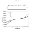
- FIGS. 10 and 11 are diagrams showing experimental structures for explaining ohmic contact characteristics and schottky contact characteristics by forming a metal that forms an ohmic contact and a metal that forms a schottky contact on a second conductive type semiconductor layer, and experimental results thereof, according to an embodiment of the invention. These are non-limiting examples for explaining the invention and the advantages associated thereto.
- a plurality of ohmic metal layers 91 (one example of a current blocking layer) and a plurality of schottky metal layers 71 (another example of a current blocking layer) are formed on a p-type GaN layer 51 (example of second conductive type semiconductor layer 50), respectively, where the plurality of ohmic metal layers 91 and the plurality of schottky metal layers 71 are spaced apart from each other.
- the interval or space 'd' between the two ohmic metal layers 91 is adjusted to be 20 ⁇ m, 30 ⁇ m, 40 ⁇ m, 60 ⁇ m, and 80 ⁇ m.
- the result of this experiment shows the ohmic barrier characteristics, as shown in FIG. 10 .
- the interval 'd' between the two schottky metal layers 71 is adjusted to be 20 ⁇ m, 30 ⁇ m, 40 ⁇ m, 60 ⁇ m, and 80 ⁇ m.
- the result of this experiment shows schottky barrier characteristics, as shown in FIG. 11 .
- the ohmic barrier characteristics and the schottky barrier characteristics are shown and vary according to the kind of metal (current blocking layer) contacting the second conductive type semiconductor layer 50.
- the current blocking layer 70 having the schottky barrier characteristics is formed on a position overlapped with (or substantially aligned with) the first electrode layer 100 in the vertical direction, thereby preventing the current from concentratedly flowing in the vertical direction from only a certain potion of the second electrode layer 90 to the lower side of the first electrode layer 100 and thereby allowing the current to more widely flow to the second conductive type semiconductor layer 50, the active layer 40 and the first conductive type semiconductor layer 30.
- the current concentration phenomenon where the current flows concentratedly to the lower side of the first electrode layer 100 can be prevented so that the light emitting device can be driven at stable operation voltages.
- the current concentration phenomenon when the current flows concentratedly to the lower side of the first electrode layer 100, light is mainly generated from the area of the active layer 40 positioned under the lower side of the first electrode layer 100.
- the light generated from the active layer 40 under the first electrode layer 100 is absorbed by the first electrode layer 100 so that the quantity of light is highly likely to be decreased or to be disappeared in the light emitting device.
- the light emitting device according to the embodiment has improve optical efficiency and is effective.
- the current blocking layers 70 are formed on the peripheral portions of the second electrode layer 90. As a result, current flowing to the peripheral portions adjacent to the side surface of the light emitting device can be reduced and accordingly, the leakage current of the light emitting device can be also reduced.
- FIGS. 1 to 5 are diagrams explaining a light emitting device according to the first embodiment, and a method for manufacturing the same.
- a un-doped GaN layer 20, a first conductive type semiconductor layer 30, an active layer 40, and a second conductive type semiconductor layer 50 are formed on a substrate 10. Also, a buffer layer (not shown) may further be formed between the substrate 10 and the un-doped GaN layer 20.
- the substrate 10 may be formed of at least one of sapphire (Al 2 O 3 ), Si, SiC, GaAs, ZnO, and MgO.
- the buffer layer may be formed in a multi layer having a stacked structure such as AlInN/GaN, In x Ga 1-x N/GaN, Al x InyGa 1-w-y N/In x Ga 1-x N/GaN, etc., and for example, it may grow by implanting trimethylgallium (TMGa), trimethylindium (TMIn), and trimethylaluminum (TMA1) into the chamber, together with hydrogen gas and ammonium gas.
- TMGa trimethylgallium
- TMIn trimethylindium
- TMA1 trimethylaluminum
- the un-doped GaN layer 20 may grow by implanting trimethylgallium (TMGa) into the chamber, together with hydrogen gas and ammonium gas.
- TMGa trimethylgallium
- the first conductive type semiconductor layer 30 may be a nitride semiconductor layer implanted with first conductive type impurity ions, for example, a semiconductor layer implanted with n-type impurity ions.
- the first conductive semiconductor layer 30 may grow by implanting trimethylgallium (TMGa) and siren gas (SiN 4 ) including n-type impurity (for example, Si) into the chamber, together with hydrogen gas and ammonium gas.
- TMGa trimethylgallium
- SiN 4 siren gas
- the active layer 40 and second conductive type semiconductor layer 50 are formed on the first conductive type semiconductor layer 30.
- the active layer 40 may be formed in a single-quantum well structure or in a multi-quantum well structure, for example, in a stacked structure of InGaN well layer/GaN barrier layer.
- the second conductive type semiconductor layer 50 may be a nitride semiconductor layer implanted with second conductive type impurity ions, for example, a semiconductor layer implanted with p-type impurity ions.
- the second conductive type semiconductor layer 50 may grow by implanting trimethylgallium (TMGa) and bisethylcyclopentadienyl magnesium (EtCp 2 Mg) ⁇ Mg(C 2 HsCsH 4 ) 2 ⁇ into the chamber, together with hydrogen gas and ammonium gas.
- TMGa trimethylgallium
- EtCp 2 Mg bisethylcyclopentadienyl magnesium
- mask layers 60 are formed on the second conductive type semiconductor layer 50.
- the mask layers 60 are used for selectively forming the current blocking layers 70 on the second conductive type semiconductor layer 50.
- the metal that forms a schottky contact may use at least one of titanium (Ti), zirconium (Zr), chrome (Cr), gold (Au) or tungsten (W).
- the second electrode layer 90 is formed on the second conductive type semiconductor layer 50 and the current blocking layers 70.
- the second electrode layer 90 may include an ohmic contact layer, a reflective layer, and a conductive substrate.
- the ohmic contact layer may be formed on the second conductive type semiconductor layer 50 and the current blocking layers 70, and the reflective electrode layer and the conductive substrate may be formed on the ohmic contact layer.
- the conductive substrate or the reflective layer having the ohmic contact characteristics may be formed directly on the second conductive type semiconductor layer 50.
- the substrate 10 and the un-doped GaN layer 20 are removed.
- the buffer layer is also removed.
- the first electrode layer 100 is formed on the first conductive type semiconductor layer 30.
- the first electrode layer 100 may be formed of at least one of copper (Cu), titanium (Ti), chrome (Cr), nickel (Ni), aluminum (Al), platinum (Pt), or gold (Au).
- the light emitting device according to the first embodiment can be manufactured.
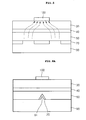
- FIG. 6A is a diagram explaining a light emitting device according to a second embodiment.
- the light emitting device includes a second electrode layer 90 that includes a projection part 91, a current blocking layer 70 formed on the projection part 91, a second conductive type semiconductor layer 50 formed on the second electrode layer 90 and the current blocking layer 70, an active layer 40 formed on the second conductive type semiconductor layer 50, a first conductive type semiconductor layer 30 formed on the active layer 40, and a first electrode layer 100 formed on the first conductive type semiconductor layer 30.
- the current blocking layer 70 is formed between the second electrode layer 90 and the second conductive semiconductor layer 50, thereby changing the path of current flowing in the light emitting device.
- the current blocking layer 70 includes a metal that forms a schottky contact with the second conductive type semiconductor layer 50.
- the current blocking layer 70 may be formed of at least one of titanium (Ti), zirconium (Zr), chrome (Cr), gold (Au) or tungsten (W), or an alloy including at least one of titanium (Ti), zirconium (Zr), chrome (Cr), gold (Au) or tungsten (W).
- At least a portion of the projection part 91 may be disposed to be overlapped with (or correspond with) the first electrode layer 100 in the vertical direction, and accordingly, at least a portion of the current blocking layer 70 may be disposed on the projection part 91 to overlap with or correspond with the first electrode layer 100 in the vertical direction.
- the first electrode layer 100 may be formed on a central portion of the first conductive type semiconductor layer 30, and the current blocking layer 70 may be formed under the first electrode layer 100, e.g., on the central portion of the second electrode layer 90.
- At least a portion of the current blocking layer 70 is disposed on the same horizontal plane with the second conductive type semiconductor layer 50, and at least a portion of the second electrode layer 90 is disposed on the same horizontal plane with the second conductive type semiconductor layer 50. Also, at least portions of the current blocking layer 70, the second electrode layer 90, and the second conductive type semiconductor layer 50 may be disposed on the same horizontal plane.
- the current blocking layer 70 serves to change the flow of current as in the light emitting device according to the first embodiment.
- the current blocking layer 70 is formed on the projection part 91, the light emitted from the active layer 40 is scattered by the current blocking layer 70, making it possible to improve the light extraction efficiency of the light emitting device.
- the current blocking layer 70 may be formed by forming a groove (or indentation) by selectively etching the second conductive type semiconductor layer 50 and then burying a material having schottky contact characteristics with the second conductive type semiconductor layer 50 in the groove. And then, a second electrode layer 90 is formed on the current blocking layer 70 and the second conductive type semiconductor layer 50, thereby making it possible to form the light emitting device having the structure as shown in FIG. 6 .
- the shape and size of the projection part 91 and the current blocking layer 70 may vary and the present invention encompasses such variations. For instance, the current blocking layer 70 may be in the shape of a "U" or "V" or a mere indentation.
- FIG. 6B illustrates a variation of the light emitting device of FIG. 6A according to the second embodiment.
- the current blocking layer 70 of FIG. 6B is formed directly on the flat part or coplanar surface of the second electrode 90, and can have a substantially triangular shape.
- the current blocking layer 70 of FIG. 6B can have a triangular/pyramid shape or an upside-down triangular/pyramid shape or some other shape.
- FIG. 7 is a diagram explaining a light emitting device according to a third embodiment.
- the light emitting device has current blocking layers that are a combination of the current blocking layers of the first and second embodiments.
- the current blocking layers 70 are formed on a central portion and peripheral portion(s) of the second electrode layer 90. Similarly, a projection part 91 is formed on the central portion of the second electrode layer 90 to be overlapped with (or correspond with) the first electrode layer 100 in the vertical direction, and the current blocking layer 70 is formed on the projection part 91.
- the current blocking layer 70 formed on the central portion of the second electrode layer 90 is formed in the similar shape as the current blocking layer 70 of the light emitting device according to the second embodiment, and the current blocking layer(s) 70 formed on the peripheral portion(s) of the second electrode layer 90 are formed in the similar shape as the current blocking layers 70 according to the first embodiment.
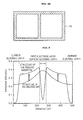
- FIG. 8A is a diagram explaining a light emitting device according to a fourth embodiment
- FIG. 8B is a top plan view of the light emitting device of FIG. 8A cut along a dotted line 8B-8B in FIG. 8A as a variation.
- the light emitting device according to the fourth embodiment has the shape similar with the light emitting device according to the second embodiment.
- the current blocking layers 70 are formed on a central portion and peripheral portion(s) of the second electrode 90.
- a projection part 91 is formed on the central portion of the second electrode layer 90 to be overlapped with or correspond with the first electrode layer 100 in the vertical direction, and the current blocking layer 70 is formed on the projection part 91.
- additional projection part(s) 91 are formed on the peripheral portion(s) on the second electrode layer 90, and additional current blocking layer(s) 70 are formed on the projection part(s) 91 to correspond with the additional projection part(s) 91.
- a window pattern or the like as shown in the top plan view of the current blocking layer(s) 70 in FIG. 8B may be formed by the current blocking layer(s) 70.
- the current blocking layer(s) 70 may be formed to surround only a part of the periphery of the second electrode 90, and thus may not completely surround it. All the current blocking layers 70 can have the same or similar shape and/or size to each other, or may have varying shapes and/or sizes.
- the current blocking layer can be formed with a non-metal or nonconductive material, e.g., SiO 2 or similar compound or material, other insulating material, ITO, ZnO, or IrO, etc.
- a non-metal or nonconductive material e.g., SiO 2 or similar compound or material, other insulating material, ITO, ZnO, or IrO, etc.
- FIG. 9 is a diagram explaining light extraction characteristics of a light emitting device according to embodiments.
- X axis represents distance from a left sided end of the light emitting device to a right sided end thereof in the cross sectional view of FIG. 5 , wherein the current blocking layers 70 are disposed on portions corresponding to 0 to 50 ⁇ m, 225 to 275 ⁇ m, and 450 to 550 ⁇ m.
- Y axis represents values that relatively represent the quantity of light extracted from the light emitting device on the assumption that the quantity of light generated from the light emitting devise is 1.
- the structure of the light emitting device in the related art means a structure where the current blocking layers 70 does not exist and are not formed between the second conductive type semiconductor layer 50 and the second electrode layer 90.
- more current flows towards the central portion so that the greatest quantity of light is generated and extracted from the area of the active layer 40 overlapped with the first electrode layer 100 in the vertical direction.
- the light generated from the area of the active layer 40 overlapped with the first electrode layer 100 in the vertical direction is absorbed by the first electrode layer 100 so that the quantity of light is highly likely to be decreased or to be disappeared in the light emitting device.
- any reference in this specification to "one embodiment,” “an embodiment,” “example embodiment,” etc. means that a particular feature, structure, or characteristic described in connection with the embodiment is included in at least one embodiment of the invention.
- the appearances of such phrases in various places in the specification are not necessarily all referring to the same embodiment.
Landscapes
- Led Devices (AREA)
- Electrodes Of Semiconductors (AREA)
Priority Applications (1)
| Application Number | Priority Date | Filing Date | Title |
|---|---|---|---|
| EP12183239.8A EP2533308B1 (fr) | 2008-11-24 | 2009-11-18 | Dispositif électroluminescent |
Applications Claiming Priority (1)
| Application Number | Priority Date | Filing Date | Title |
|---|---|---|---|
| KR1020080116751A KR101047634B1 (ko) | 2008-11-24 | 2008-11-24 | 발광 소자 및 그 제조방법 |
Related Child Applications (2)
| Application Number | Title | Priority Date | Filing Date |
|---|---|---|---|
| EP12183239.8A Division-Into EP2533308B1 (fr) | 2008-11-24 | 2009-11-18 | Dispositif électroluminescent |
| EP12183239.8A Division EP2533308B1 (fr) | 2008-11-24 | 2009-11-18 | Dispositif électroluminescent |
Publications (2)
| Publication Number | Publication Date |
|---|---|
| EP2190036A1 true EP2190036A1 (fr) | 2010-05-26 |
| EP2190036B1 EP2190036B1 (fr) | 2012-10-10 |
Family
ID=41611206
Family Applications (2)
| Application Number | Title | Priority Date | Filing Date |
|---|---|---|---|
| EP09014384A Not-in-force EP2190036B1 (fr) | 2008-11-24 | 2009-11-18 | Dispositif électroluminescent et son procédé de fabrication |
| EP12183239.8A Not-in-force EP2533308B1 (fr) | 2008-11-24 | 2009-11-18 | Dispositif électroluminescent |
Family Applications After (1)
| Application Number | Title | Priority Date | Filing Date |
|---|---|---|---|
| EP12183239.8A Not-in-force EP2533308B1 (fr) | 2008-11-24 | 2009-11-18 | Dispositif électroluminescent |
Country Status (4)
| Country | Link |
|---|---|
| US (2) | US8288786B2 (fr) |
| EP (2) | EP2190036B1 (fr) |
| KR (1) | KR101047634B1 (fr) |
| CN (1) | CN101740695B (fr) |
Cited By (1)
| Publication number | Priority date | Publication date | Assignee | Title |
|---|---|---|---|---|
| WO2016165983A1 (fr) * | 2015-04-15 | 2016-10-20 | Koninklijke Philips N.V. | Dispositif électroluminescent à réflecteur et à contact supérieur |
Families Citing this family (22)
| Publication number | Priority date | Publication date | Assignee | Title |
|---|---|---|---|---|
| KR101047634B1 (ko) * | 2008-11-24 | 2011-07-07 | 엘지이노텍 주식회사 | 발광 소자 및 그 제조방법 |
| TWI484671B (zh) * | 2010-01-14 | 2015-05-11 | Wen Pin Chen | 發光二極體及其製造方法 |
| KR101039937B1 (ko) * | 2010-04-28 | 2011-06-09 | 엘지이노텍 주식회사 | 발광소자, 발광소자의 제조방법, 발광소자 패키지 및 조명시스템 |
| KR101182920B1 (ko) * | 2010-07-05 | 2012-09-13 | 엘지이노텍 주식회사 | 발광 소자 및 그 제조방법 |
| CN101937957A (zh) * | 2010-08-11 | 2011-01-05 | 中国科学院半导体研究所 | 氮化镓基垂直结构发光二极管电极结构的制作方法 |
| KR101719623B1 (ko) | 2010-09-07 | 2017-03-24 | 엘지이노텍 주식회사 | 발광소자 |
| EP2439793B1 (fr) | 2010-10-11 | 2016-03-16 | LG Innotek Co., Ltd. | Dispositif électroluminescent et instrument d'éclairage l'incluant |
| KR20120040448A (ko) * | 2010-10-19 | 2012-04-27 | 삼성엘이디 주식회사 | 수직형 발광 소자 |
| US20120097918A1 (en) * | 2010-10-20 | 2012-04-26 | Varian Semiconductor Equipment Associates, Inc. | Implanted current confinement structure to improve current spreading |
| EP2445019B1 (fr) * | 2010-10-25 | 2018-01-24 | LG Innotek Co., Ltd. | Configuration d'électrode pour une diode électroluminescente |
| KR20120131983A (ko) * | 2011-05-27 | 2012-12-05 | 삼성전자주식회사 | 전류제한층을 구비한 반도체 발광 소자 |
| US20130001510A1 (en) * | 2011-06-29 | 2013-01-03 | SemiLEDs Optoelectronics Co., Ltd. | Optoelectronic device having current blocking insulation layer for uniform temperature distribution and method of fabrication |
| JP6056154B2 (ja) * | 2011-07-21 | 2017-01-11 | 富士ゼロックス株式会社 | 発光素子、発光素子アレイ、光書込みヘッドおよび画像形成装置 |
| CN103367559A (zh) * | 2012-03-29 | 2013-10-23 | 上海蓝光科技有限公司 | 一种发光二极管及其制造方法 |
| US8816379B2 (en) | 2012-05-17 | 2014-08-26 | High Power Opto, Inc. | Reflection curved mirror structure of a vertical light-emitting diode |
| US8748928B2 (en) | 2012-05-17 | 2014-06-10 | High Power Opto, Inc. | Continuous reflection curved mirror structure of a vertical light-emitting diode |
| US8546831B1 (en) * | 2012-05-17 | 2013-10-01 | High Power Opto Inc. | Reflection convex mirror structure of a vertical light-emitting diode |
| CN103000779B (zh) * | 2012-09-24 | 2015-01-07 | 安徽三安光电有限公司 | 具有电流阻挡功能的垂直发光二极管及其制作方法 |
| KR102140278B1 (ko) * | 2014-04-18 | 2020-07-31 | 엘지이노텍 주식회사 | 발광 소자 |
| KR102153123B1 (ko) * | 2014-06-10 | 2020-10-26 | 엘지이노텍 주식회사 | 발광소자 및 이를 구비한 발광소자 패키지 |
| CN104638069A (zh) * | 2015-02-04 | 2015-05-20 | 映瑞光电科技(上海)有限公司 | 垂直型led芯片结构及其制作方法 |
| CN105609596A (zh) * | 2015-09-11 | 2016-05-25 | 映瑞光电科技(上海)有限公司 | 具有电流阻挡结构的led垂直芯片及其制备方法 |
Citations (5)
| Publication number | Priority date | Publication date | Assignee | Title |
|---|---|---|---|---|
| DE19937624A1 (de) * | 1999-07-09 | 2001-03-01 | Epistar Corp | Leuchtdiode mit einer großen Helligkeit |
| US6492661B1 (en) * | 1999-11-04 | 2002-12-10 | Fen-Ren Chien | Light emitting semiconductor device having reflection layer structure |
| US20060163588A1 (en) * | 2003-01-06 | 2006-07-27 | Showa Denko K.K | Boron phosphide-based semiconductor light-emitting device and production method thereof |
| WO2007124708A1 (fr) | 2006-04-27 | 2007-11-08 | Osram Opto Semiconductors Gmbh | Puce à semi-conducteur optoélectronique |
| US20080217635A1 (en) | 2004-06-30 | 2008-09-11 | David Todd Emerson | Light emitting devices having current reducing structures and methods of forming light emitting devices having current reducing structures |
Family Cites Families (29)
| Publication number | Priority date | Publication date | Assignee | Title |
|---|---|---|---|---|
| KR940003109B1 (ko) | 1991-04-17 | 1994-04-13 | 삼성전자 주식회사 | 화상 기록장치 |
| KR940003109A (ko) * | 1992-07-31 | 1994-02-19 | 김광호 | 발광다이오드 및 그 제조방법 |
| US5565694A (en) * | 1995-07-10 | 1996-10-15 | Huang; Kuo-Hsin | Light emitting diode with current blocking layer |
| JP3787195B2 (ja) * | 1996-09-06 | 2006-06-21 | シャープ株式会社 | 窒化ガリウム系化合物半導体発光素子の製造方法 |
| JPH10294531A (ja) * | 1997-02-21 | 1998-11-04 | Toshiba Corp | 窒化物化合物半導体発光素子 |
| JP4083866B2 (ja) * | 1998-04-28 | 2008-04-30 | シャープ株式会社 | 半導体レーザ素子 |
| DE19937524A1 (de) | 1999-08-03 | 2001-02-15 | Harald Martin | Verfahren und Vorrichtung zum Beseitigen von Abprodukten und Abfallstoffen |
| JP2001274456A (ja) * | 2000-01-18 | 2001-10-05 | Sharp Corp | 発光ダイオード |
| JP2001223384A (ja) * | 2000-02-08 | 2001-08-17 | Toshiba Corp | 半導体発光素子 |
| US6462661B2 (en) * | 2000-11-20 | 2002-10-08 | Seagate Technology Llc | RF ID tag attachment to a disc drive |
| JP2003046119A (ja) | 2001-07-26 | 2003-02-14 | Hitachi Cable Ltd | 発光ダイオード及びその製造方法 |
| JP4148494B2 (ja) * | 2001-12-04 | 2008-09-10 | シャープ株式会社 | 窒化物系化合物半導体発光素子およびその製造方法 |
| US6784462B2 (en) * | 2001-12-13 | 2004-08-31 | Rensselaer Polytechnic Institute | Light-emitting diode with planar omni-directional reflector |
| JP2004047760A (ja) | 2002-07-12 | 2004-02-12 | Hitachi Cable Ltd | 発光ダイオード用エピタキシャルウェハ及び発光ダイオード |
| JP2004288799A (ja) * | 2003-03-20 | 2004-10-14 | Sony Corp | 半導体発光素子およびその製造方法、集積型半導体発光装置およびその製造方法、画像表示装置およびその製造方法ならびに照明装置およびその製造方法 |
| TWI270991B (en) * | 2004-01-16 | 2007-01-11 | Epistar Corp | Organic adhesive light-emitting device with ohmic metal contact |
| TWI244220B (en) * | 2004-02-20 | 2005-11-21 | Epistar Corp | Organic binding light-emitting device with vertical structure |
| DE102004026231B4 (de) * | 2004-05-28 | 2019-01-31 | Osram Opto Semiconductors Gmbh | Verfahren zur Herstellung eines Bereichs mit reduzierter elektrischer Leitfähigkeit innerhalb einer Halbleiterschicht und optoelektronisches Halbleiterbauelement |
| US7335920B2 (en) * | 2005-01-24 | 2008-02-26 | Cree, Inc. | LED with current confinement structure and surface roughening |
| KR100723150B1 (ko) * | 2005-12-26 | 2007-05-30 | 삼성전기주식회사 | 수직구조 질화물 반도체 발광소자 및 제조방법 |
| KR100673640B1 (ko) | 2006-01-09 | 2007-01-24 | 삼성전기주식회사 | 수직구조 질화갈륨계 발광다이오드 소자 |
| KR100752696B1 (ko) | 2006-02-16 | 2007-08-29 | 삼성전기주식회사 | 수직구조 질화갈륨계 발광다이오드 소자 |
| KR100856089B1 (ko) | 2006-08-23 | 2008-09-02 | 삼성전기주식회사 | 수직구조 질화갈륨계 발광 다이오드 소자 및 그 제조방법 |
| KR100867529B1 (ko) * | 2006-11-14 | 2008-11-10 | 삼성전기주식회사 | 수직형 발광 소자 |
| KR101008287B1 (ko) * | 2006-12-30 | 2011-01-13 | 주식회사 에피밸리 | 3족 질화물 반도체 발광소자 |
| US8124991B2 (en) * | 2007-07-26 | 2012-02-28 | The Regents Of The University Of California | Light emitting diodes with a P-type surface bonded to a transparent submount to increase light extraction efficiency |
| US20090242929A1 (en) * | 2008-03-31 | 2009-10-01 | Chao-Kun Lin | Light emitting diodes with patterned current blocking metal contact |
| JP5638514B2 (ja) * | 2008-04-30 | 2014-12-10 | エルジー イノテック カンパニー リミテッド | 発光素子及びその製造方法 |
| KR101047634B1 (ko) * | 2008-11-24 | 2011-07-07 | 엘지이노텍 주식회사 | 발광 소자 및 그 제조방법 |
-
2008
- 2008-11-24 KR KR1020080116751A patent/KR101047634B1/ko not_active Expired - Fee Related
-
2009
- 2009-11-06 US US12/614,240 patent/US8288786B2/en active Active
- 2009-11-18 EP EP09014384A patent/EP2190036B1/fr not_active Not-in-force
- 2009-11-18 EP EP12183239.8A patent/EP2533308B1/fr not_active Not-in-force
- 2009-11-24 CN CN200910226190.8A patent/CN101740695B/zh not_active Expired - Fee Related
-
2012
- 2012-09-14 US US13/618,952 patent/US8569784B2/en not_active Expired - Fee Related
Patent Citations (5)
| Publication number | Priority date | Publication date | Assignee | Title |
|---|---|---|---|---|
| DE19937624A1 (de) * | 1999-07-09 | 2001-03-01 | Epistar Corp | Leuchtdiode mit einer großen Helligkeit |
| US6492661B1 (en) * | 1999-11-04 | 2002-12-10 | Fen-Ren Chien | Light emitting semiconductor device having reflection layer structure |
| US20060163588A1 (en) * | 2003-01-06 | 2006-07-27 | Showa Denko K.K | Boron phosphide-based semiconductor light-emitting device and production method thereof |
| US20080217635A1 (en) | 2004-06-30 | 2008-09-11 | David Todd Emerson | Light emitting devices having current reducing structures and methods of forming light emitting devices having current reducing structures |
| WO2007124708A1 (fr) | 2006-04-27 | 2007-11-08 | Osram Opto Semiconductors Gmbh | Puce à semi-conducteur optoélectronique |
Cited By (2)
| Publication number | Priority date | Publication date | Assignee | Title |
|---|---|---|---|---|
| WO2016165983A1 (fr) * | 2015-04-15 | 2016-10-20 | Koninklijke Philips N.V. | Dispositif électroluminescent à réflecteur et à contact supérieur |
| US10026881B2 (en) | 2015-04-15 | 2018-07-17 | Koninklijke Philips N.V. | Light emitting device with reflector and a top contact |
Also Published As
| Publication number | Publication date |
|---|---|
| US8288786B2 (en) | 2012-10-16 |
| KR101047634B1 (ko) | 2011-07-07 |
| KR20100058072A (ko) | 2010-06-03 |
| US8569784B2 (en) | 2013-10-29 |
| US20100127303A1 (en) | 2010-05-27 |
| EP2533308A2 (fr) | 2012-12-12 |
| CN101740695A (zh) | 2010-06-16 |
| CN101740695B (zh) | 2014-06-11 |
| EP2190036B1 (fr) | 2012-10-10 |
| US20130009198A1 (en) | 2013-01-10 |
| EP2533308A3 (fr) | 2013-05-29 |
| EP2533308B1 (fr) | 2019-02-27 |
Similar Documents
| Publication | Publication Date | Title |
|---|---|---|
| EP2190036B1 (fr) | Dispositif électroluminescent et son procédé de fabrication | |
| US9142729B2 (en) | Light emitting element | |
| KR101493321B1 (ko) | 전류 분산 효과가 우수한 발광소자 및 그 제조 방법 | |
| KR101039896B1 (ko) | 발광소자 및 그 제조방법 | |
| EP2290707B1 (fr) | Dispositif électroluminescent à semi-conducteur | |
| US10121939B2 (en) | Semiconductor light-emitting devices and methods of manufacturing the same | |
| US8492782B2 (en) | Semiconductor light emitting device | |
| KR101103963B1 (ko) | 발광소자 및 그 제조방법 | |
| CN110931619A (zh) | 倒装led芯片及其制造方法 | |
| WO2002071450A2 (fr) | Fil conducteur de del destine a une extraction de lumiere amelioree | |
| JP2007214569A (ja) | フリップチップ型の発光素子 | |
| US9812614B2 (en) | Light-emitting device | |
| KR100952034B1 (ko) | 발광 소자 및 그 제조방법 | |
| JP5989318B2 (ja) | 半導体発光素子及びその製造方法 | |
| US8008684B2 (en) | Light emitting device and method for manufacturing the same | |
| KR20120055332A (ko) | 발광소자 및 발광소자 패키지 | |
| KR20120052747A (ko) | 발광소자 및 그 제조방법 | |
| KR20130113268A (ko) | 발광효율이 우수한 발광소자 어레이 | |
| KR20120065676A (ko) | 발광소자의 제조방법 | |
| KR102153123B1 (ko) | 발광소자 및 이를 구비한 발광소자 패키지 | |
| KR20120049694A (ko) | 발광소자 및 발광소자 패키지 | |
| KR20120017935A (ko) | 발광소자 |
Legal Events
| Date | Code | Title | Description |
|---|---|---|---|
| PUAI | Public reference made under article 153(3) epc to a published international application that has entered the european phase |
Free format text: ORIGINAL CODE: 0009012 |
|
| AK | Designated contracting states |
Kind code of ref document: A1 Designated state(s): AT BE BG CH CY CZ DE DK EE ES FI FR GB GR HR HU IE IS IT LI LT LU LV MC MK MT NL NO PL PT RO SE SI SK SM TR |
|
| AX | Request for extension of the european patent |
Extension state: AL BA RS |
|
| RAP1 | Party data changed (applicant data changed or rights of an application transferred) |
Owner name: LG INNOTEK CO., LTD. |
|
| 17P | Request for examination filed |
Effective date: 20101124 |
|
| GRAP | Despatch of communication of intention to grant a patent |
Free format text: ORIGINAL CODE: EPIDOSNIGR1 |
|
| RIN1 | Information on inventor provided before grant (corrected) |
Inventor name: HWANG, SUNG MIN Inventor name: PARK, GYEONG GEUN Inventor name: CHO, HYUN KYONG |
|
| GRAS | Grant fee paid |
Free format text: ORIGINAL CODE: EPIDOSNIGR3 |
|
| GRAA | (expected) grant |
Free format text: ORIGINAL CODE: 0009210 |
|
| AK | Designated contracting states |
Kind code of ref document: B1 Designated state(s): AT BE BG CH CY CZ DE DK EE ES FI FR GB GR HR HU IE IS IT LI LT LU LV MC MK MT NL NO PL PT RO SE SI SK SM TR |
|
| REG | Reference to a national code |
Ref country code: GB Ref legal event code: FG4D |
|
| REG | Reference to a national code |
Ref country code: AT Ref legal event code: REF Ref document number: 579304 Country of ref document: AT Kind code of ref document: T Effective date: 20121015 Ref country code: CH Ref legal event code: EP |
|
| REG | Reference to a national code |
Ref country code: IE Ref legal event code: FG4D |
|
| REG | Reference to a national code |
Ref country code: NL Ref legal event code: T3 |
|
| REG | Reference to a national code |
Ref country code: DE Ref legal event code: R096 Ref document number: 602009010278 Country of ref document: DE Effective date: 20121206 |
|
| PG25 | Lapsed in a contracting state [announced via postgrant information from national office to epo] |
Ref country code: SI Free format text: LAPSE BECAUSE OF FAILURE TO SUBMIT A TRANSLATION OF THE DESCRIPTION OR TO PAY THE FEE WITHIN THE PRESCRIBED TIME-LIMIT Effective date: 20121010 |
|
| REG | Reference to a national code |
Ref country code: AT Ref legal event code: MK05 Ref document number: 579304 Country of ref document: AT Kind code of ref document: T Effective date: 20121010 |
|
| REG | Reference to a national code |
Ref country code: LT Ref legal event code: MG4D |
|
| PG25 | Lapsed in a contracting state [announced via postgrant information from national office to epo] |
Ref country code: LT Free format text: LAPSE BECAUSE OF FAILURE TO SUBMIT A TRANSLATION OF THE DESCRIPTION OR TO PAY THE FEE WITHIN THE PRESCRIBED TIME-LIMIT Effective date: 20121010 Ref country code: FI Free format text: LAPSE BECAUSE OF FAILURE TO SUBMIT A TRANSLATION OF THE DESCRIPTION OR TO PAY THE FEE WITHIN THE PRESCRIBED TIME-LIMIT Effective date: 20121010 Ref country code: NO Free format text: LAPSE BECAUSE OF FAILURE TO SUBMIT A TRANSLATION OF THE DESCRIPTION OR TO PAY THE FEE WITHIN THE PRESCRIBED TIME-LIMIT Effective date: 20130110 Ref country code: SE Free format text: LAPSE BECAUSE OF FAILURE TO SUBMIT A TRANSLATION OF THE DESCRIPTION OR TO PAY THE FEE WITHIN THE PRESCRIBED TIME-LIMIT Effective date: 20121010 Ref country code: IS Free format text: LAPSE BECAUSE OF FAILURE TO SUBMIT A TRANSLATION OF THE DESCRIPTION OR TO PAY THE FEE WITHIN THE PRESCRIBED TIME-LIMIT Effective date: 20130210 Ref country code: HR Free format text: LAPSE BECAUSE OF FAILURE TO SUBMIT A TRANSLATION OF THE DESCRIPTION OR TO PAY THE FEE WITHIN THE PRESCRIBED TIME-LIMIT Effective date: 20121010 Ref country code: ES Free format text: LAPSE BECAUSE OF FAILURE TO SUBMIT A TRANSLATION OF THE DESCRIPTION OR TO PAY THE FEE WITHIN THE PRESCRIBED TIME-LIMIT Effective date: 20130121 |
|
| PG25 | Lapsed in a contracting state [announced via postgrant information from national office to epo] |
Ref country code: BE Free format text: LAPSE BECAUSE OF FAILURE TO SUBMIT A TRANSLATION OF THE DESCRIPTION OR TO PAY THE FEE WITHIN THE PRESCRIBED TIME-LIMIT Effective date: 20121010 Ref country code: PL Free format text: LAPSE BECAUSE OF FAILURE TO SUBMIT A TRANSLATION OF THE DESCRIPTION OR TO PAY THE FEE WITHIN THE PRESCRIBED TIME-LIMIT Effective date: 20121010 Ref country code: LV Free format text: LAPSE BECAUSE OF FAILURE TO SUBMIT A TRANSLATION OF THE DESCRIPTION OR TO PAY THE FEE WITHIN THE PRESCRIBED TIME-LIMIT Effective date: 20121010 Ref country code: PT Free format text: LAPSE BECAUSE OF FAILURE TO SUBMIT A TRANSLATION OF THE DESCRIPTION OR TO PAY THE FEE WITHIN THE PRESCRIBED TIME-LIMIT Effective date: 20130211 Ref country code: GR Free format text: LAPSE BECAUSE OF FAILURE TO SUBMIT A TRANSLATION OF THE DESCRIPTION OR TO PAY THE FEE WITHIN THE PRESCRIBED TIME-LIMIT Effective date: 20130111 |
|
| PG25 | Lapsed in a contracting state [announced via postgrant information from national office to epo] |
Ref country code: AT Free format text: LAPSE BECAUSE OF FAILURE TO SUBMIT A TRANSLATION OF THE DESCRIPTION OR TO PAY THE FEE WITHIN THE PRESCRIBED TIME-LIMIT Effective date: 20121010 |
|
| PG25 | Lapsed in a contracting state [announced via postgrant information from national office to epo] |
Ref country code: DK Free format text: LAPSE BECAUSE OF FAILURE TO SUBMIT A TRANSLATION OF THE DESCRIPTION OR TO PAY THE FEE WITHIN THE PRESCRIBED TIME-LIMIT Effective date: 20121010 Ref country code: EE Free format text: LAPSE BECAUSE OF FAILURE TO SUBMIT A TRANSLATION OF THE DESCRIPTION OR TO PAY THE FEE WITHIN THE PRESCRIBED TIME-LIMIT Effective date: 20121010 Ref country code: CZ Free format text: LAPSE BECAUSE OF FAILURE TO SUBMIT A TRANSLATION OF THE DESCRIPTION OR TO PAY THE FEE WITHIN THE PRESCRIBED TIME-LIMIT Effective date: 20121010 Ref country code: BG Free format text: LAPSE BECAUSE OF FAILURE TO SUBMIT A TRANSLATION OF THE DESCRIPTION OR TO PAY THE FEE WITHIN THE PRESCRIBED TIME-LIMIT Effective date: 20130110 Ref country code: SK Free format text: LAPSE BECAUSE OF FAILURE TO SUBMIT A TRANSLATION OF THE DESCRIPTION OR TO PAY THE FEE WITHIN THE PRESCRIBED TIME-LIMIT Effective date: 20121010 |
|
| REG | Reference to a national code |
Ref country code: IE Ref legal event code: MM4A |
|
| PLBE | No opposition filed within time limit |
Free format text: ORIGINAL CODE: 0009261 |
|
| STAA | Information on the status of an ep patent application or granted ep patent |
Free format text: STATUS: NO OPPOSITION FILED WITHIN TIME LIMIT |
|
| REG | Reference to a national code |
Ref country code: FR Ref legal event code: ST Effective date: 20130731 |
|
| PG25 | Lapsed in a contracting state [announced via postgrant information from national office to epo] |
Ref country code: RO Free format text: LAPSE BECAUSE OF FAILURE TO SUBMIT A TRANSLATION OF THE DESCRIPTION OR TO PAY THE FEE WITHIN THE PRESCRIBED TIME-LIMIT Effective date: 20121010 Ref country code: IT Free format text: LAPSE BECAUSE OF FAILURE TO SUBMIT A TRANSLATION OF THE DESCRIPTION OR TO PAY THE FEE WITHIN THE PRESCRIBED TIME-LIMIT Effective date: 20121010 |
|
| 26N | No opposition filed |
Effective date: 20130711 |
|
| PG25 | Lapsed in a contracting state [announced via postgrant information from national office to epo] |
Ref country code: IE Free format text: LAPSE BECAUSE OF NON-PAYMENT OF DUE FEES Effective date: 20121118 |
|
| REG | Reference to a national code |
Ref country code: DE Ref legal event code: R097 Ref document number: 602009010278 Country of ref document: DE Effective date: 20130711 |
|
| PG25 | Lapsed in a contracting state [announced via postgrant information from national office to epo] |
Ref country code: MT Free format text: LAPSE BECAUSE OF FAILURE TO SUBMIT A TRANSLATION OF THE DESCRIPTION OR TO PAY THE FEE WITHIN THE PRESCRIBED TIME-LIMIT Effective date: 20121010 Ref country code: CY Free format text: LAPSE BECAUSE OF FAILURE TO SUBMIT A TRANSLATION OF THE DESCRIPTION OR TO PAY THE FEE WITHIN THE PRESCRIBED TIME-LIMIT Effective date: 20121010 Ref country code: FR Free format text: LAPSE BECAUSE OF NON-PAYMENT OF DUE FEES Effective date: 20121210 |
|
| PG25 | Lapsed in a contracting state [announced via postgrant information from national office to epo] |
Ref country code: MC Free format text: LAPSE BECAUSE OF NON-PAYMENT OF DUE FEES Effective date: 20121130 Ref country code: TR Free format text: LAPSE BECAUSE OF FAILURE TO SUBMIT A TRANSLATION OF THE DESCRIPTION OR TO PAY THE FEE WITHIN THE PRESCRIBED TIME-LIMIT Effective date: 20121010 |
|
| PG25 | Lapsed in a contracting state [announced via postgrant information from national office to epo] |
Ref country code: LU Free format text: LAPSE BECAUSE OF NON-PAYMENT OF DUE FEES Effective date: 20121118 Ref country code: SM Free format text: LAPSE BECAUSE OF FAILURE TO SUBMIT A TRANSLATION OF THE DESCRIPTION OR TO PAY THE FEE WITHIN THE PRESCRIBED TIME-LIMIT Effective date: 20121010 |
|
| REG | Reference to a national code |
Ref country code: CH Ref legal event code: PL |
|
| PG25 | Lapsed in a contracting state [announced via postgrant information from national office to epo] |
Ref country code: LI Free format text: LAPSE BECAUSE OF NON-PAYMENT OF DUE FEES Effective date: 20131130 Ref country code: CH Free format text: LAPSE BECAUSE OF NON-PAYMENT OF DUE FEES Effective date: 20131130 Ref country code: HU Free format text: LAPSE BECAUSE OF FAILURE TO SUBMIT A TRANSLATION OF THE DESCRIPTION OR TO PAY THE FEE WITHIN THE PRESCRIBED TIME-LIMIT Effective date: 20091118 |
|
| PG25 | Lapsed in a contracting state [announced via postgrant information from national office to epo] |
Ref country code: MK Free format text: LAPSE BECAUSE OF FAILURE TO SUBMIT A TRANSLATION OF THE DESCRIPTION OR TO PAY THE FEE WITHIN THE PRESCRIBED TIME-LIMIT Effective date: 20121010 |
|
| PGFP | Annual fee paid to national office [announced via postgrant information from national office to epo] |
Ref country code: GB Payment date: 20161007 Year of fee payment: 8 Ref country code: NL Payment date: 20161007 Year of fee payment: 8 |
|
| REG | Reference to a national code |
Ref country code: NL Ref legal event code: MM Effective date: 20171201 |
|
| GBPC | Gb: european patent ceased through non-payment of renewal fee |
Effective date: 20171118 |
|
| PG25 | Lapsed in a contracting state [announced via postgrant information from national office to epo] |
Ref country code: NL Free format text: LAPSE BECAUSE OF NON-PAYMENT OF DUE FEES Effective date: 20171201 |
|
| PG25 | Lapsed in a contracting state [announced via postgrant information from national office to epo] |
Ref country code: GB Free format text: LAPSE BECAUSE OF NON-PAYMENT OF DUE FEES Effective date: 20171118 |
|
| PGFP | Annual fee paid to national office [announced via postgrant information from national office to epo] |
Ref country code: DE Payment date: 20181005 Year of fee payment: 10 |
|
| REG | Reference to a national code |
Ref country code: DE Ref legal event code: R119 Ref document number: 602009010278 Country of ref document: DE |
|
| PG25 | Lapsed in a contracting state [announced via postgrant information from national office to epo] |
Ref country code: DE Free format text: LAPSE BECAUSE OF NON-PAYMENT OF DUE FEES Effective date: 20200603 |