EP2190060A2 - Radiofrequenzidentifikations (RFID)-Etikett und Herstellungsverfahren dafür - Google Patents
Radiofrequenzidentifikations (RFID)-Etikett und Herstellungsverfahren dafür Download PDFInfo
- Publication number
- EP2190060A2 EP2190060A2 EP20100152269 EP10152269A EP2190060A2 EP 2190060 A2 EP2190060 A2 EP 2190060A2 EP 20100152269 EP20100152269 EP 20100152269 EP 10152269 A EP10152269 A EP 10152269A EP 2190060 A2 EP2190060 A2 EP 2190060A2
- Authority
- EP
- European Patent Office
- Prior art keywords
- chip
- dielectric member
- rfid tag
- antenna pattern
- dielectric
- Prior art date
- Legal status (The legal status is an assumption and is not a legal conclusion. Google has not performed a legal analysis and makes no representation as to the accuracy of the status listed.)
- Withdrawn
Links
Images







Classifications
-
- G—PHYSICS
- G06—COMPUTING OR CALCULATING; COUNTING
- G06K—GRAPHICAL DATA READING; PRESENTATION OF DATA; RECORD CARRIERS; HANDLING RECORD CARRIERS
- G06K19/00—Record carriers for use with machines and with at least a part designed to carry digital markings
- G06K19/06—Record carriers for use with machines and with at least a part designed to carry digital markings characterised by the kind of the digital marking, e.g. shape, nature, code
- G06K19/067—Record carriers with conductive marks, printed circuits or semiconductor circuit elements, e.g. credit or identity cards also with resonating or responding marks without active components
- G06K19/07—Record carriers with conductive marks, printed circuits or semiconductor circuit elements, e.g. credit or identity cards also with resonating or responding marks without active components with integrated circuit chips
- G06K19/077—Constructional details, e.g. mounting of circuits in the carrier
-
- H—ELECTRICITY
- H01—ELECTRIC ELEMENTS
- H01Q—ANTENNAS, i.e. RADIO AERIALS
- H01Q23/00—Antennas with active circuits or circuit elements integrated within them or attached to them
-
- G—PHYSICS
- G06—COMPUTING OR CALCULATING; COUNTING
- G06K—GRAPHICAL DATA READING; PRESENTATION OF DATA; RECORD CARRIERS; HANDLING RECORD CARRIERS
- G06K19/00—Record carriers for use with machines and with at least a part designed to carry digital markings
- G06K19/06—Record carriers for use with machines and with at least a part designed to carry digital markings characterised by the kind of the digital marking, e.g. shape, nature, code
- G06K19/067—Record carriers with conductive marks, printed circuits or semiconductor circuit elements, e.g. credit or identity cards also with resonating or responding marks without active components
- G06K19/07—Record carriers with conductive marks, printed circuits or semiconductor circuit elements, e.g. credit or identity cards also with resonating or responding marks without active components with integrated circuit chips
-
- G—PHYSICS
- G06—COMPUTING OR CALCULATING; COUNTING
- G06K—GRAPHICAL DATA READING; PRESENTATION OF DATA; RECORD CARRIERS; HANDLING RECORD CARRIERS
- G06K19/00—Record carriers for use with machines and with at least a part designed to carry digital markings
- G06K19/06—Record carriers for use with machines and with at least a part designed to carry digital markings characterised by the kind of the digital marking, e.g. shape, nature, code
- G06K19/067—Record carriers with conductive marks, printed circuits or semiconductor circuit elements, e.g. credit or identity cards also with resonating or responding marks without active components
- G06K19/07—Record carriers with conductive marks, printed circuits or semiconductor circuit elements, e.g. credit or identity cards also with resonating or responding marks without active components with integrated circuit chips
- G06K19/077—Constructional details, e.g. mounting of circuits in the carrier
- G06K19/07749—Constructional details, e.g. mounting of circuits in the carrier the record carrier being capable of non-contact communication, e.g. constructional details of the antenna of a non-contact smart card
-
- G—PHYSICS
- G06—COMPUTING OR CALCULATING; COUNTING
- G06K—GRAPHICAL DATA READING; PRESENTATION OF DATA; RECORD CARRIERS; HANDLING RECORD CARRIERS
- G06K19/00—Record carriers for use with machines and with at least a part designed to carry digital markings
- G06K19/06—Record carriers for use with machines and with at least a part designed to carry digital markings characterised by the kind of the digital marking, e.g. shape, nature, code
- G06K19/067—Record carriers with conductive marks, printed circuits or semiconductor circuit elements, e.g. credit or identity cards also with resonating or responding marks without active components
- G06K19/07—Record carriers with conductive marks, printed circuits or semiconductor circuit elements, e.g. credit or identity cards also with resonating or responding marks without active components with integrated circuit chips
- G06K19/077—Constructional details, e.g. mounting of circuits in the carrier
- G06K19/07749—Constructional details, e.g. mounting of circuits in the carrier the record carrier being capable of non-contact communication, e.g. constructional details of the antenna of a non-contact smart card
- G06K19/07771—Constructional details, e.g. mounting of circuits in the carrier the record carrier being capable of non-contact communication, e.g. constructional details of the antenna of a non-contact smart card the record carrier comprising means for minimising adverse effects on the data communication capability of the record carrier, e.g. minimising Eddy currents induced in a proximate metal or otherwise electromagnetically interfering object
-
- H—ELECTRICITY
- H01—ELECTRIC ELEMENTS
- H01Q—ANTENNAS, i.e. RADIO AERIALS
- H01Q1/00—Details of, or arrangements associated with, antennas
- H01Q1/12—Supports; Mounting means
- H01Q1/22—Supports; Mounting means by structural association with other equipment or articles
- H01Q1/2208—Supports; Mounting means by structural association with other equipment or articles associated with components used in interrogation type services, i.e. in systems for information exchange between an interrogator/reader and a tag/transponder, e.g. in Radio Frequency Identification [RFID] systems
-
- H—ELECTRICITY
- H01—ELECTRIC ELEMENTS
- H01Q—ANTENNAS, i.e. RADIO AERIALS
- H01Q1/00—Details of, or arrangements associated with, antennas
- H01Q1/12—Supports; Mounting means
- H01Q1/22—Supports; Mounting means by structural association with other equipment or articles
- H01Q1/2208—Supports; Mounting means by structural association with other equipment or articles associated with components used in interrogation type services, i.e. in systems for information exchange between an interrogator/reader and a tag/transponder, e.g. in Radio Frequency Identification [RFID] systems
- H01Q1/2216—Supports; Mounting means by structural association with other equipment or articles associated with components used in interrogation type services, i.e. in systems for information exchange between an interrogator/reader and a tag/transponder, e.g. in Radio Frequency Identification [RFID] systems used in interrogator/reader equipment
-
- H—ELECTRICITY
- H01—ELECTRIC ELEMENTS
- H01Q—ANTENNAS, i.e. RADIO AERIALS
- H01Q1/00—Details of, or arrangements associated with, antennas
- H01Q1/12—Supports; Mounting means
- H01Q1/22—Supports; Mounting means by structural association with other equipment or articles
- H01Q1/2208—Supports; Mounting means by structural association with other equipment or articles associated with components used in interrogation type services, i.e. in systems for information exchange between an interrogator/reader and a tag/transponder, e.g. in Radio Frequency Identification [RFID] systems
- H01Q1/2225—Supports; Mounting means by structural association with other equipment or articles associated with components used in interrogation type services, i.e. in systems for information exchange between an interrogator/reader and a tag/transponder, e.g. in Radio Frequency Identification [RFID] systems used in active tags, i.e. provided with its own power source or in passive tags, i.e. deriving power from RF signal
-
- H—ELECTRICITY
- H01—ELECTRIC ELEMENTS
- H01Q—ANTENNAS, i.e. RADIO AERIALS
- H01Q7/00—Loop antennas with a substantially uniform current distribution around the loop and having a directional radiation pattern in a plane perpendicular to the plane of the loop
-
- H—ELECTRICITY
- H10—SEMICONDUCTOR DEVICES; ELECTRIC SOLID-STATE DEVICES NOT OTHERWISE PROVIDED FOR
- H10W—GENERIC PACKAGES, INTERCONNECTIONS, CONNECTORS OR OTHER CONSTRUCTIONAL DETAILS OF DEVICES COVERED BY CLASS H10
- H10W72/00—Interconnections or connectors in packages
- H10W72/071—Connecting or disconnecting
- H10W72/072—Connecting or disconnecting of bump connectors
- H10W72/07251—Connecting or disconnecting of bump connectors characterised by changes in properties of the bump connectors during connecting
-
- H—ELECTRICITY
- H10—SEMICONDUCTOR DEVICES; ELECTRIC SOLID-STATE DEVICES NOT OTHERWISE PROVIDED FOR
- H10W—GENERIC PACKAGES, INTERCONNECTIONS, CONNECTORS OR OTHER CONSTRUCTIONAL DETAILS OF DEVICES COVERED BY CLASS H10
- H10W72/00—Interconnections or connectors in packages
- H10W72/20—Bump connectors, e.g. solder bumps or copper pillars; Dummy bumps; Thermal bumps
-
- Y—GENERAL TAGGING OF NEW TECHNOLOGICAL DEVELOPMENTS; GENERAL TAGGING OF CROSS-SECTIONAL TECHNOLOGIES SPANNING OVER SEVERAL SECTIONS OF THE IPC; TECHNICAL SUBJECTS COVERED BY FORMER USPC CROSS-REFERENCE ART COLLECTIONS [XRACs] AND DIGESTS
- Y10—TECHNICAL SUBJECTS COVERED BY FORMER USPC
- Y10T—TECHNICAL SUBJECTS COVERED BY FORMER US CLASSIFICATION
- Y10T29/00—Metal working
- Y10T29/49—Method of mechanical manufacture
- Y10T29/49002—Electrical device making
- Y10T29/49117—Conductor or circuit manufacturing
-
- Y—GENERAL TAGGING OF NEW TECHNOLOGICAL DEVELOPMENTS; GENERAL TAGGING OF CROSS-SECTIONAL TECHNOLOGIES SPANNING OVER SEVERAL SECTIONS OF THE IPC; TECHNICAL SUBJECTS COVERED BY FORMER USPC CROSS-REFERENCE ART COLLECTIONS [XRACs] AND DIGESTS
- Y10—TECHNICAL SUBJECTS COVERED BY FORMER USPC
- Y10T—TECHNICAL SUBJECTS COVERED BY FORMER US CLASSIFICATION
- Y10T29/00—Metal working
- Y10T29/49—Method of mechanical manufacture
- Y10T29/49002—Electrical device making
- Y10T29/49117—Conductor or circuit manufacturing
- Y10T29/49124—On flat or curved insulated base, e.g., printed circuit, etc.
Definitions
- the present invention relates to a radio frequency identification (RFID) tag such as a non-contact integrated circuit (IC) card, which receives power supply and information from, and transmits information to, an external device.
- RFID tag emodying the present invention is also known to one skilled in the art as an “RFID tag inlay", inlay being an internal constituent part (inlay) used in the "RFID tag”.
- RFID tag is also known as a “wireless IC tag”.
- RFID tags such as a non-contact integrated circuit that receive using radio waves, power supply and information from an external device such as an IC card reader/writer and then transmit the received information to the external device contact-free are being used in recent years.
- a typical RFID tag includes an antenna pattern and an integrated circuit (IC) chip.
- the antenna pattern which transmits and receives data, is mounted on a substrate made of plastic, paper, and the like.
- the antenna pattern and a capacity element built into the IC chip form a resonance circuit, and the RFID tag communicates via radio waves with the external device by means of the antenna pattern.
- Fig. 26 and Fig. 27 are drawings of previously considered, well-known means, that enhance the gain of an antenna.
- Fig. 26 is a cross-sectional view of a previously proposed RFID tag in which a plane antenna is provided on the wave-absorbing material.
- Fig. 27 is a cross-sectional view of a conventional RFID tag in which a loop antenna is provided on the wave-absorbing material.
- a substrate 110 having a plane antenna 120 is fixed to a wave-absorbing material 100 by means of an adhesive 140.
- the plane antenna 120 is connected by means of a feeding point 130 to an IC chip (not shown) mounted on another substrate.
- An RFID tag with a plane coil antenna includes a dielectric antenna substrate and an antenna coil.
- the antenna coil includes a first set of coils located on one surface of the antenna substrate and a second set of coils located on a second surface of the antenna substrate.
- the first set of coils and the second set of coils straddle the antenna substrate, each coil of the first set and each coil of the second set alternating with each other such that a portion of the two coils face each other.
- the first set of coils and the second set of coils are connected in a predetermined sequence.
- a loop antenna 160 which is in a sheet of a metal, is fixed on the wave-absorbing material 100 by means of the adhesive 140.
- the loop antenna 160 encloses a hollow interior 150 and is connected by means of the feeding point 130 to an IC chip (not shown) mounted on another substrate.
- the RFID loop antenna is widely used in pagers.
- an antenna pattern that has a small area can be employed. If the area of the antenna pattern is small, the communication distance is short. The wave-absorbing material 100 causes further degradation of antenna response because it absorbs the radio waves.
- the antenna response is affected and the communication distance also decreases significantly in the case of the RFID tag fabricated using a plane coil antenna disclosed in Japanese Patent Laid-Open Publication No. 2004-206479 , since the wave-absorbing material 100 absorbs the radio waves.
- the loop antenna 160 may get crushed when subjected to external pressure since it has a hollow interior 150.
- Embodiments of the present invention seek to alleviate the problems encountered in the known technology.
- An RFID tag embodying an aspect of the present invention includes a dielectric member; an antenna pattern formed on and around a surface of the dielectric member whereby the antenna pattern forms a loop; and an IC chip with a built-in communication circuit and a built-in memory circuit, the IC chip being electrically connected to the antenna pattern.
- An RFID tag embodying another aspect of the present invention includes a dielectric member; a film substrate that includes an antenna pattern, the film substrate being tied on and around the dielectric member whereby the antenna pattern forms a loop; and an IC chip with a built-in communication circuit and a built-in memory circuit, the IC chip being electrically connected to the antenna pattern.
- An RFID tag embodying a still further aspect of the present invention includes a dielectric member; a dielectric member support that slidably supports the dielectric member; a film substrate that includes an antenna pattern, the film substrate being tied on and around the dielectric member whereby the antenna pattern forms a loop; and an IC chip with a built-in communication circuit and a built-in memory circuit, the IC chip being electrically connected to the antenna pattern.
- An RFID tag manufacturing method embodying a still further aspect of the present invention includes mounting a film substrate having a transceiving antenna pattern on a surface of a dielectric member and forming a loop antenna; and electrically connecting an IC chip to the antenna pattern, the IC chip including at least a built-in communication circuit and a built-in memory circuit.
- An RFID tag manufacturing method embodying another aspect of the present invention includes forming a loop antenna on a surface of a dielectric member by means of a transceiving antenna pattern; and electrically connecting an IC chip to the antenna pattern, the IC chip including a built-in communication circuit and a built-in memory circuit.
- An RFID tag manufacturing method embodying another aspect of the present invention includes electrically connecting an IC chip to a first transceiving antenna pattern of a first film substrate, wherein the IC chip includes a built-in communication circuit and a built-in memory circuit; laminating a first surface of a dielectric member with the first film substrate such that the IC chip mounted on the first film substrate fits into a concavity provided on the dielectric member; laminating a second surface of the dielectric member with a second film substrate having a second transceiving antenna pattern; and electrically connecting the first transceiving antenna pattern of the first film substrate and the second transceiving antenna pattern of the second film substrate by means of a conductive member.
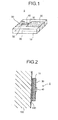
- Fig. 1 is a perspective view of the RFID tag according to a first embodiment of the present invention.
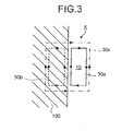
- Fig. 2 is a cross-sectional view of the RFID tag mounted on a wave-absorbing material.
- Fig. 3 is a schematic diagram that illustrates a principle of the formation of a large current loop.
- a RFID tag 5 according to the first embodiment of the present invention includes a rectangular dielectric member 10, an antenna pattern 30 that transmits and receives data, and an integrated circuit (IC) chip 40.
- the antenna pattern 30 is a loop antenna tied around the surface of the dielectric member 10.
- the IC chip 40 is electrically connected to the antenna pattern 30 via chip pads 32.
- the rectangular dielectric member 10 is composed of a dielectric material having a certain dielectric constant, and may be a high frequency substrate composed of resin containing glass, etc.
- the antenna pattern 30 on the plane surface of the dielectric member 10 is formed by etching a conductor (for instance, a metallic conductor such as copper).
- a pair of chip pads 32 on which an IC chip 40 is mounted and that electrically connect the IC chip 40 to the antenna pattern 30 is also formed by etching along with the antenna pattern 30.
- the antenna pattern 30 on the side surfaces (thickness of the dielectric member) of the dielectric member 10 is formed by a known side conduction method of plating.
- the IC chip 40 includes a communication circuit that records and reads the information contact-free, a memory, and a designated control circuit.
- the IC chip 40 also includes chip electrodes that electrically connect the IC chip 40 to the chip pads 32 that extend to the antenna pattern 30.
- the control circuit may not necessarily be provided within the IC chip 40.
- the antenna pattern 30 and the chip pads 32 are formed on the dielectric member 10 by etching process and the like to form a loop antenna (loop antenna formation step).
- the IC chip 40 mounting step is carried out next.
- the IC chip 40 is mounted in such a way that the chip electrodes of the IC chip 40 are electrically connected to the chip pads 32.
- a flip chip mount can be used as a mounting means.
- the RFID tag 5 is secured on a wave-absorbing material 100 such as a wine bottle using the adhesive 140 (for instance, a two-sided tape) and is covered by a not shown specified protection film.
- the RFID tag 5 may be equipped beforehand with the protection film and the adhesive 140 in order to be secured to the article in which it is to be used.
- the antenna pattern 30 forms a small loop antenna 30a around the dielectric member 10.
- the small loop antenna 30a also forms an image current 30b on the wave-absorbing material 100.
- the small loop antenna 30a and the image current 30b form a large current loop 30c.
- the formation of the large current loop 30c enhances the transmission gain and significantly increases the communication distance. In other words, reduction of communication distance can be controlled.
- the antenna pattern 30 since the antenna pattern 30 is formed on the dielectric member 10, the antenna pattern 30 does not get damaged even when it is subjected to external pressure.
- the RFID tag 5 that has a structure as described above that can transmit accurate radio wave information due to enhanced transmission gain of the antenna when receiving power supply and information from and transmitting the received information to an external device (not shown) contact-free. As a result, the reliability of the data communication can be increased.
- a rectangular dielectric member 10 has been used in the RFID tag 5 according to the first embodiment, the dielectric member 10 may be of any shape (for instance, cylindrical, triangular prism, spherical, etc.) depending on the article it is intended for.
- Fig. 4 is a perspective view of a RFID tag according to a second embodiment of the present invention.
- Fig. 5 is a top view of a film substrate.
- the parts in the second embodiment that are identical to those in the first embodiment are assigned the same reference numerals and their description is made very brief or skipped altogether.
- the RFID tag 5 includes the dielectric member 10, a film substrate 20, and the IC chip 40.
- the film substrate 20 forms the antenna pattern 30 that transmits and receives data and is wrapped around the dielectric member 10.
- the IC chip 40 is connected to the antenna pattern 30.
- the rectangular dielectric member 10 is composed of a dielectric material that has a designated dielectric constant and can be formed inexpensively using only glass-free resin.
- the dielectric member 10 can be formed with resin such as polytetrafluoroethylene (PTFE), polyphenylether (PPE), and the like, that have excellent processibility and mechanical properties.
- PTFE polytetrafluoroethylene
- PPE polyphenylether
- the antenna pattern 30 that forms the transceiving loop antenna is formed on the film substrate 20 by a printing means.
- the film substrate 20 is composed of a flexible thermoplastic material.
- Polyethylene terephthalate (hereinafter, "PET"), polyimide (PI), polyethylene naphthalate (PEN), and polyvinyl chloride (PVC) can be used as material for the film substrate 20.
- PET is the most suitable material for the film substrate 20.
- the dimensions of the film substrate are in proportion to the dielectric member 10 such that the loop antenna can be formed by means of the antenna pattern 30.
- the antenna pattern 30 is formed by silk screen printing a conductive paste over the film substrate 20.
- the film substrate 20 includes the chip pads 32 on which the IC chip 40 is connected and that electrically connect the IC chip 40 to the antenna pattern 30.
- the chip pads 32 are simultaneously formed along with the antenna pattern 30 by silk screen printing the conductive paste on the film substrate 20.
- the manufacturing method of the RFID tag 5 is explained next.
- the film substrate 20 that includes the antenna pattern 30 is wrapped around the dielectric member 10 by bending at folds 22 corresponding to the edges of the dielectric member 10.
- the film substrate 20 is secured to the dielectric member 10 by means of an adhesive or a two-sided tape.
- the loop antenna is thus formed. This is the loop antenna formation step in the manufacturing method of the RFID tag 5.
- the IC chip 40 mounting step is carried out next.
- the IC chip 40 is mounted in such a way that the chip electrodes of the IC chip 40 are electrically connected to the chip pads 32.
- a flip chip mount can be used as the mounting means.
- the RFID tag 5 according to the second embodiment of the present invention can be easily and inexpensively manufactured by wrapping the film substrate 20 that includes the antenna pattern 30 around the inexpensive dielectric member 10 having a good processibility and by mounting the IC chip 40 on the chip pads 32.
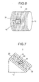
- the dielectric member 10 may be, for instance, cylindrical, triangular prism, spherical, etc., depending on the article it is intended for.
- the film substrate 20 may be wrapped around a cylindrical dielectric member 10.
- the film substrate 20 may be wrapped around a triangular prism-shaped dielectric member 10. The effect produced in all the above case will be the same as for the second embodiment.
- Fig. 6, Fig. 7 , and Fig. 8 are perspective views of RFID tags having different shapes.
- Fig. 9 is a perspective view of the RFID tag according to a third embodiment of the present invention.
- Fig. 10 is a top view of the film substrate.
- the chip pad 32 is provided parallel to the length of the antenna pattern 30 in such a way that the position of the feeding point of the IC chip 40 can be adjusted.
- the chip pad 32 is connected to the antenna pattern 30 by a connector 32a and is provided parallel to the antenna pattern 30.
- the chip pad 32 and the connector 32a are composed of the same material as the antenna pattern 30 and are simultaneously formed when the antenna pattern 30 is printed on the film substrate 20.
- the film substrate 20 is wrapped around and secured to the dielectric member 10 in such a way that the antenna pattern 30 functions as a patch antenna.
- the IC chip 40 is mounted after the film substrate 20 is secured to the dielectric member 10 and the position of the feeding point is adjusted.
- the position of the feeding point is adjusted by electrically connecting the chip electrode of the IC chip 40 to the chip pad 32 and the antenna pattern 30, sliding the IC chip 40 along the length (that is, in the direction of the arrow shown in the drawing) of the chip pad 32, and changing the mounting location of the IC chip 40.
- the IC chip 40 is mounted there.
- a flip chip mount can be used as the mounting means.
- the RFID tag 5 allows the antenna response to be adjusted by adjusting the position of the feeding point by changing the mounting location of the IC chip 40.
- Fig. 11 is a perspective view of the RFID tag according to a fourth embodiment of the present invention.
- Fig. 12 is a top view of the film substrate. Though the antenna pattern 30 is actually on the underside of the film substrate 20, to facilitate explanation, the antenna pattern 30 is shown in Fig. 12 in X-ray view (that is, as appearing to be on the surface of the film substrate 20).
- the chip pad 32 is provided on the film substrate 20 in such a way that the position of the feeding point can be easily adjusted by changing the mounting location of the IC chip 40.
- an inverted T-shaped film substrate extension 20a is provided from the film substrate 20 and the chip pad 32 is set on the film substrate extension 20a along the length of and parallel to the antenna pattern 30 in such a way that the position of the feeding point of the IC chip 40 to the antenna pattern 30 can be adjusted.
- the film substrate 20 and the film substrate extension 20a are wrapped around and secured to the dielectric member 10 in such a way that the antenna pattern 30 functions as a patch antenna.
- the rest of the structure of the RFID tag and the method of adjustment of the mounting location of the IC chip 40 are identical to those according to the third embodiment and hence are not described here.
- the RFID tag 5 allows the antenna response to be adjusted by adjusting the position of the feeding point by changing the mounting location of the IC chip 40.
- Fig. 13 is a perspective view of the RFID tag according to a fifth embodiment of the present invention.
- a depressed portion 10a is provided on a surface of the dielectric member 10 and the film substrate 20 is fit in it. This configuration facilitates alignment of the film substrate 20 with the dielectric member 10.
- the depth of the depressed portion 10a is substantially equal to the sum of the thickness of the film substrate 20 and the thickness of the IC chip 40.
- the surface of the mounted IC chip 40 sits in the depressed portion 10a without jutting out of the surface of the dielectric member 10.
- the rest of the structure and the manufacturing method of the RFID tag 5 is identical to that of the RFID tag 5 according to the second embodiment, and hence are not described here.
- the RFID tag 5 according to the fifth embodiment of the present invention allows the film substrate 20 to be easily aligned with the dielectric member 10 by providing the depressed portion 10a on the dielectric member 10.
- the RFID tag 5 Since the surface of the mounted IC chip 40 sits in the concave portion 10a and does not jut out of the surface of the dielectric member 10, when secured to an article such as a wave-absorbing material and is covered with the protection film the RFID tag 5 remains safe without any pressure being transferred to it. Consequently, the durability of the RFID tag 5 against external pressure is enhanced.
- this flat RFID tag 5 is ideal for using on the inner lining of clothing and apparel since it does not poke when coming in contact with the body.
- the fifth embodiment can be applied to all the embodiments that follow (in case of a ninth embodiment, which is described later, a depressed portion having the same functions as the depressed portion 10a may be provided on a dielectric member support 60, which is described later). However, all the embodiments produce the same effect.
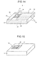
- Fig. 14 is a perspective view of the RFID tag according to a sixth embodiment of the present invention.
- Fig. 15 is a perspective view of the RFID tag in which the IC chip is mounted on the chip pads formed on the dielectric member.
- chip pads 12 are already provided on the side of the dielectric member 10 and the IC chip 40 is mounted on the chip pads 12.
- the film substrate 20 is wrapped around the dielectric member 10 in such a way that the antenna pattern 30 printed on the bottom surface (underside) of the film substrate 20 is electrically connected to the chip pads 12.
- the chip pads 12 can be formed on the dielectric member 10 by etching copper, by printing a conductive ink, or by pasting a conductive material.
- the connection of the chip pads 12 to the antenna pattern 30 and securing of one to the other can be done by applying a conductive adhesive (silver paste) on the contact surfaces of the chip pads 12 and the antenna pattern 30 and then applying pressure and heat on the portion.
- a conductive adhesive silver paste
- the mounting method of the IC chip 40 and the wrapping method of the film substrate 20 are identical to those according to the second embodiment, and hence are not described here.
- the RFID tag 5 allows the selection of the film substrate 20 that includes the antenna pattern 30 most suited to the mounted IC chip 40, thus enabling adjustment of the transmission and reception response.
- Fig. 16 is a perspective view of the RFID tag according to a seventh embodiment of the present invention.
- Fig. 17 is a top view of the film substrate.
- the IC chip 40 is mounted on a side surface of the dielectric member 10. In other words, the IC chip 40 is mounted in such a location that a bulge due to the presence of the IC chip 40 is avoided in the largest plane portion of the RFID tag 5.
- the film substrate 20 is formed in such a way that the IC chip 40 can be mounted on the side surface of the dielectric member 10.
- a pair of film substrate extensions 20b of the film substrate 20 and a pair of chip pads 32 extend towards a side of the dielectric member 10.
- the chip pads 32 are printed on the film substrate extensions 20b in continuity with the antenna pattern 30.
- the mounting method of the IC chip 40 and the wrapping method of the film substrate 20 are identical to those according to the second embodiment, they are not described here.
- the IC chip 40 is mounted on a side surface of the dielectric member 10. Consequently, a bulge due to the presence of the IC chip 40 is avoided in the largest plane portion of the RFID tag 5.
- setting the IC chip 40 on the side surface makes the RFID tag 5 safe without any pressure being transferred to it when secured to an article and covered with the protection film. Consequently, the durability of the RFID tag 5 against external pressure is enhanced. Further, this flat RFID tag 5 is ideal for using on the inner lining of clothing and apparel since it does not poke when coming in contact with the body.
- the dielectric member 10 may be of any shape (for instance, cylindrical, triangular prism, spherical, etc.) depending the article it is intended for.
- the film substrate 20 may be wrapped around a cylindrical dielectric member 10 and the IC chip 40 is provided on the disk portion of the cylinder.
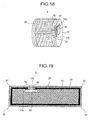
- Fig. 18 is a perspective view of an RFID tag having a different shape.
- Fig. 19 is a perspective view of the RFID tag according to an eighth embodiment of the present invention.
- a concavity 10b into which the IC chip 40 can be accommodated is provided on the dielectric member 10 and the IC chip 40 is set in the concavity 10b.
- the film substrate 20 is wrapped around the dielectric member 10 in such a way that and the IC chip 40 is electrically connected to the antenna pattern 30 formed on the underside of the film substrate 20.
- the RFID tag 5 is fabricated in such a way that the IC chip 40 does not jut out of the surface of the RFID tag 5.
- Bumps 50 are provided on the chip electrodes (not shown) of the IC chip 40.
- the IC chip 40 is fixed to the bottom of the concavity 10b, with the bumps 50 facing upward, by means of a thermosetting adhesive or an instant adhesive.
- the IC chip 40 is covered with an underfill 52 so as to keep the IC chip 40 and the bumps 50 securely held and protected.
- the film substrate 20 is wrapped and secured around the dielectric member 10 in such a way that the antenna pattern 30 and the bumps 50 of the IC chip 40 are electrically connected.
- connection of the bumps 50 with the antenna pattern 30 and the securing of one to the other can be done by applying the conductive adhesive (silver paste) on the contact surfaces of the bumps 50 and the antenna patterns 30 and then applying pressure and heat on the portion.
- the conductive adhesive silver paste
- the RFID tag 5 according to the eighth embodiment of the present invention has a plane surface since the IC chip 40 fits inside the concavity 10b of the dielectric member 10
- accommodating the IC chip 40 makes the RFID tag 5 safe without any pressure being transferred to it when secured to an article and covered with the protection film. Consequently, the durability of the RFID tag 5 against external pressure is enhanced. Further, this flat RFID tag 5 is ideal for using on the inner lining of clothing and apparel since it does not poke when coming in contact with the body.
- the film substrate 20 is wrapped around the dielectric member 10 in such a way that the concavity 10b is in aligned against the length edge of the film substrate 20.
- the film substrate 20 may be wrapped around the dielectric member 10 in such a way that the concavity 10b is in aligned against the width edge of the film substrate 20.
- Fig. 20 is a perspective view of the RFID tag according to the ninth embodiment of the present invention.
- Fig. 21 is a perspective view of the RFID tag in which the dielectric member is secured to a dielectric member support.
- the RFID tag 5 according to the ninth embodiment includes the dielectric member 10, the dielectric member support 60 that slidably supports the dielectric member 10, the film substrate 20 that is wrapped around the surface of the dielectric member 10 and including the antenna pattern 30, and the IC chip 40 that is electrically connected to the antenna pattern 30.
- the dielectric member support 60 which may be composed of resin, such as plastic, has a slot 62 for sliding the dielectric member 10 in and out of.
- the dielectric constant of the dielectric member is adjusted by sliding the dielectric member 10 in the dielectric member support 60 in the direction of the arrow shown in Fig. 20 .
- the response of the antenna can be adjusted easily by adjusting the dielectric constant.
- the dielectric member 10 and the dielectric member support 60 are secured with an adhesive 70 to maintain the position of the adjusted dielectric member 10.
- the dielectric member 10 can be secured by applying the adhesive 70 on edge at the opening of the slot 62.
- the adhesive may be applied inside the slot 62 instead of at the opening.
- a notch means may be used as a securing means wherein a lug and notches that engage into each other may be provided and the position of engagement may be changed by application of a certain degree of external pressure.
- the mounting method of the IC chip 40 and the wrapping method of the film substrate 20 are identical to those described in the second embodiment, and hence are not described here.
- the RFID tag 5 according to the ninth embodiment of the present invention allows adjustment of the dielectric constant, and hence the response of the antenna, by sliding the dielectric member 10 in and out of the dielectric member support 60.
- the RFID tag can be easily inactivated (that is, communication can be disabled). To inactivate the RFID tag 5 all a user needs to do is remove the adhesive 70 and remove the dielectric member 10 from the dielectric member support 60.
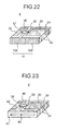
- Fig. 22 is a perspective view of the RFID tag according to a tenth embodiment of the present invention.
- the dielectric member 10 is composed of a plurality of dielectric members 10A and 10B that have different dielectric constants and dielectric losses in order to adjust the dielectric constant and a dielectric loss.
- the dielectric member 10A with a high dielectric constant and dielectric loss and the dielectric member 10B with a low dielectric constant and dielectric loss are combined (the dielectric members 10A and 10B are integrated by gluing them together), the dielectric member 10 with intermediate properties can be obtained.
- the dielectric members 10A and 10B are combined horizontally in Fig. 22 . However, the dielectric members 10A and 10B may also be combined vertically (that is, in the thickness direction of the dielectric members).
- the mounting method of the IC chip 40 and the wrapping method of the film substrate 20 are identical to those described in the second embodiment, and hence not described here.
- the RFID tag 5 allows adjustment of the dielectric constant and the dielectric loss, and hence the response of the antenna, by using the dielectric member 10 formed by combing dielectric members 10A and 10B having different dielectric constants and dielectric losses.
- the tenth embodiment can also be applied to first through eighth embodiments as well as a twelfth embodiment described later to produce identical effect.
- Fig. 23 is a perspective view of the RFID tag according to an eleventh embodiment of the present invention.
- the RFID tag 5 according to the eleventh embodiment has a structure similar to the RFID tag 5 according to the second embodiment except that the dielectric member 10 has an airspace 80.
- the airspace 80 is a vacant space that forms a layer of air of predetermined thickness within the dielectric member 10. In other words, the dielectric constant in the dielectric member 10 can be reduced and set to the desired value by the dielectric constant of the air in the airspace 80.
- the RFID tag 5 allows antenna response to be easily adjusted by adjusting the dielectric constant of the dielectric member 10 by increasing or decreasing the airspace 80 within the dielectric member 10.
- the eleventh embodiment is explained by taking the RFID tag 5 according to the second embodiment and providing the airspace 80 in the dielectric member 10. It is also possible to provide the airspace 80 in the dielectric member 10 of the RFID tag 5 according to any of the first embodiment, third to eighth embodiments, and the twelfth embodiment explained next.
- Fig. 24 is a cross-sectional view of the RFID tag according to a twelfth embodiment of the present invention.
- Fig. 25 is a cross-sectional view of the RFID tag to illustrate a lamination step.
- the RFID tag 5 is formed by mounting the IC chip 40 on the concavity 10b of the dielectric member 10 and a single sheet of the film substrate 20 is wrapped around the dielectric member 10 to form folds 22, as shown in fig. 19 .
- the RFID tag 5 is fabricated by laminating the surface and the underside of the dielectric member 10 by two separate film substrates 20, as shown in Fig. 24 and Fig. 25 .
- the manufacturing method of the RFID tag 5 includes two steps, namely the IC chip mounting process and the lamination process.
- the IC chip mounting process involves electrically connecting the antenna pattern 30 of a first film substrate 20 to the IC chip 40.
- the lamination process involves fixing the first film substrate 20 on the surface (a first surface) of the dielectric member 10 in such a way that the IC chip 40 sits in the concavity 10b of the dielectric member 10, fixing a second film substrate 20 on the underside (a second surface) of the dielectric member 10, and forming the loop antenna by electrically connecting the two antenna patterns 30 of two film substrates 20 by means of a conductive adhesive (conductive member) 24, such as silver paste.
- a conductive adhesive conductive member
- the flip chip mount can be used in the IC chip mounting step.
- the lamination of the two film substrates 20 and the connection of the antenna patterns 30 in the lamination step are carried out by applying pressure and heat on the portion having the conductive adhesive 24, as indicated by the arrows in Fig. 25 .
- adhesive is used on the contact surfaces of the dielectric member 10 and the film substrate 20 other than in the portions where the conductive adhesive 24 is provided.
- the lamination of the film substrates 20 and the connection of the antenna patterns 30 in the lamination step in the RFID tag 5 according to the twelfth embodiment of the present invention can be done more easily than wrapping the film substrate 20 around the dielectric member 10 as in the eighth embodiment.
- the IC chip 40 is laminated by the film substrates 20, the need to provide a special lamination (protection film) to protect the RFID tag 5 is obviated, reducing the number of components.
- a loop antenna is formed on a surface of a dielectric member. Consequently, the transmission gain of the antenna can be enhanced and communication distance can be increased. Moreover, since an antenna pattern is formed around the dielectric member, the antenna pattern does not get damaged even when subjected to external pressure, ensuring a reliable communication.
- a film substrate that forms the loop antenna by virtue of being mounted on the surface of the dielectric member. Consequently, the loop antenna can be formed easily and inexpensively, the transmission gain of the loop antenna can be enhanced, and the communication distance can be increased. Further, since the film substrate, which includes the antenna pattern, is formed on the dielectric member, the antenna pattern does not get damaged even when subjected to external pressure, ensuring a reliable communication.
- the mounting of an IC chip and its connection to the antenna pattern can be realized simultaneously and with ease.
- the mounting of an IC chip and its connection to the antenna pattern can be realized simultaneously and with ease.
- the mounted IC chip sits inside a concavity provided in the dielectric member without jutting out of the surface of the dielectric member. Consequently, the IC chip remains safe against external pressure and the RFID tag is not easily damaged.
- the surfaces other than the side surface on which the IC chip is mounted are plane. Consequently, the IC chip remains safe against external pressure and the RFID tag is not easily damaged.
- the position of a feeding point can be adjusted easily by changing the mounting location of the IC chip on the chip pad. Consequently, the response of the antenna can be adjusted.
- the response of the antenna can be easily adjusted by sliding the dielectric member in and out of a dielectric member support.
- the antenna response can be adjusted by adjusting the dielectric constant and the dielectric loss by combining a plurality of dielectric members having different dielectric constants and dielectric losses.
- the loop antenna can be easily formed by mounting the film substrate on the surface of the dielectric member using a loop antenna formation step.
- the RFID can be easily and inexpensively manufactured by mounting the IC chip on the loop antenna using an IC chip mounting step.
Landscapes
- Engineering & Computer Science (AREA)
- Physics & Mathematics (AREA)
- Computer Hardware Design (AREA)
- Microelectronics & Electronic Packaging (AREA)
- General Physics & Mathematics (AREA)
- Theoretical Computer Science (AREA)
- Electromagnetism (AREA)
- Details Of Aerials (AREA)
- Burglar Alarm Systems (AREA)
- Credit Cards Or The Like (AREA)
- Waveguide Aerials (AREA)
- Support Of Aerials (AREA)
Applications Claiming Priority (2)
| Application Number | Priority Date | Filing Date | Title |
|---|---|---|---|
| JP2004236155A JP4653440B2 (ja) | 2004-08-13 | 2004-08-13 | Rfidタグおよびその製造方法 |
| EP04257704A EP1626364B1 (de) | 2004-08-13 | 2004-12-10 | Rfid-etikett und verfahren zu dessen herstellung |
Related Parent Applications (1)
| Application Number | Title | Priority Date | Filing Date |
|---|---|---|---|
| EP04257704.9 Division | 2004-12-10 |
Publications (2)
| Publication Number | Publication Date |
|---|---|
| EP2190060A2 true EP2190060A2 (de) | 2010-05-26 |
| EP2190060A3 EP2190060A3 (de) | 2010-06-09 |
Family
ID=35429235
Family Applications (3)
| Application Number | Title | Priority Date | Filing Date |
|---|---|---|---|
| EP08155290A Ceased EP1947733A1 (de) | 2004-08-13 | 2004-12-10 | Radiofrequenzidentifikations (RFID)-Etikett und Herstellungsverfahren dafür |
| EP20100152269 Withdrawn EP2190060A3 (de) | 2004-08-13 | 2004-12-10 | Radiofrequenzidentifikations (RFID)-Etikett und Herstellungsverfahren dafür |
| EP04257704A Expired - Lifetime EP1626364B1 (de) | 2004-08-13 | 2004-12-10 | Rfid-etikett und verfahren zu dessen herstellung |
Family Applications Before (1)
| Application Number | Title | Priority Date | Filing Date |
|---|---|---|---|
| EP08155290A Ceased EP1947733A1 (de) | 2004-08-13 | 2004-12-10 | Radiofrequenzidentifikations (RFID)-Etikett und Herstellungsverfahren dafür |
Family Applications After (1)
| Application Number | Title | Priority Date | Filing Date |
|---|---|---|---|
| EP04257704A Expired - Lifetime EP1626364B1 (de) | 2004-08-13 | 2004-12-10 | Rfid-etikett und verfahren zu dessen herstellung |
Country Status (7)
| Country | Link |
|---|---|
| US (2) | US7342498B2 (de) |
| EP (3) | EP1947733A1 (de) |
| JP (1) | JP4653440B2 (de) |
| KR (1) | KR100799140B1 (de) |
| CN (1) | CN1734478A (de) |
| DE (1) | DE602004028462D1 (de) |
| TW (1) | TWI267788B (de) |
Families Citing this family (192)
| Publication number | Priority date | Publication date | Assignee | Title |
|---|---|---|---|---|
| KR101107555B1 (ko) * | 2004-01-22 | 2012-01-31 | 미코 코포레이션 | 모듈러 무선 주파수 식별 태깅 방법 |
| KR20100021665A (ko) * | 2004-12-14 | 2010-02-25 | 후지쯔 가부시끼가이샤 | 안테나 및 비접촉형 태그 |
| DE602005024441D1 (de) | 2005-01-07 | 2010-12-09 | Fujitsu Ltd | Tag-einrichtung, antenne und tragbare karte |
| US7712674B1 (en) * | 2005-02-22 | 2010-05-11 | Eigent Technologies Llc | RFID devices for verification of correctness, reliability, functionality and security |
| CN101156162B (zh) * | 2005-03-31 | 2012-05-16 | 株式会社半导体能源研究所 | 无线芯片以及具有无线芯片的电子设备 |
| JP4750455B2 (ja) * | 2005-04-15 | 2011-08-17 | 富士通株式会社 | Rfidタグセット、rfidタグ、およびrfidタグ部品 |
| WO2006118293A1 (en) | 2005-04-27 | 2006-11-09 | Semiconductor Energy Laboratory Co., Ltd. | Wireless chip |
| TW200707301A (en) * | 2005-05-25 | 2007-02-16 | Ibm | ID tag package and RFID system |
| US20070182559A1 (en) * | 2005-09-15 | 2007-08-09 | Zih Corp. | Rfid antenna on multiple sides of 3-d packaging |
| US9361568B2 (en) | 2005-12-09 | 2016-06-07 | Tego, Inc. | Radio frequency identification tag with hardened memory system |
| JP4815207B2 (ja) * | 2005-12-13 | 2011-11-16 | 株式会社サトー | Rfidラベル |
| US20070159340A1 (en) * | 2006-01-09 | 2007-07-12 | Yuen Foong Yu Paper Mfg. Co., Ltd. | Structure and method for packaging radio frequency identification devices |
| US20070159337A1 (en) * | 2006-01-12 | 2007-07-12 | Sdgi Holdings, Inc. | Modular RFID tag |
| US9130602B2 (en) | 2006-01-18 | 2015-09-08 | Qualcomm Incorporated | Method and apparatus for delivering energy to an electrical or electronic device via a wireless link |
| US7519328B2 (en) | 2006-01-19 | 2009-04-14 | Murata Manufacturing Co., Ltd. | Wireless IC device and component for wireless IC device |
| JP5034371B2 (ja) | 2006-02-10 | 2012-09-26 | 富士通株式会社 | Rfidタグの製造方法およびrfidタグ |
| JP4755921B2 (ja) * | 2006-02-24 | 2011-08-24 | 富士通株式会社 | Rfidタグ |
| KR20080098412A (ko) | 2006-03-06 | 2008-11-07 | 미쓰비시덴키 가부시키가이샤 | Rfid태그, rfid태그의 제조 방법 및 rfid태그의 설치 방법 |
| KR100746635B1 (ko) | 2006-03-21 | 2007-08-06 | 삼성전기주식회사 | Rfid 시스템의 태그 및 그 제조 방법 |
| JP4854362B2 (ja) * | 2006-03-30 | 2012-01-18 | 富士通株式会社 | Rfidタグ及びその製造方法 |
| US9064198B2 (en) | 2006-04-26 | 2015-06-23 | Murata Manufacturing Co., Ltd. | Electromagnetic-coupling-module-attached article |
| JP5123493B2 (ja) * | 2006-05-30 | 2013-01-23 | 新光電気工業株式会社 | 配線基板及び半導体装置 |
| JP4855849B2 (ja) * | 2006-06-30 | 2012-01-18 | 富士通株式会社 | Rfidタグの製造方法、およびrfidタグ |
| JP4281850B2 (ja) | 2006-06-30 | 2009-06-17 | 株式会社村田製作所 | 光ディスク |
| JP2008009881A (ja) | 2006-06-30 | 2008-01-17 | Fujitsu Ltd | Rfidタグ製造方法およびrfidタグ |
| US8794531B2 (en) * | 2006-07-13 | 2014-08-05 | Confidex Oy | Radio frequency identification tag |
| US7589419B2 (en) * | 2006-08-07 | 2009-09-15 | Rcd Technology, Inc. | Side connectors for RFID chip |
| JP5057786B2 (ja) | 2006-08-09 | 2012-10-24 | 富士通株式会社 | タグ |
| JP5006961B2 (ja) * | 2006-09-04 | 2012-08-22 | 株式会社日立システムズ | 小型金属rfidタグ |
| JP4627537B2 (ja) * | 2006-09-04 | 2011-02-09 | 株式会社日立情報システムズ | 小型金属rfidタグを内装する金属製rfidタグ |
| DE112007002024B4 (de) | 2006-09-26 | 2010-06-10 | Murata Mfg. Co., Ltd., Nagaokakyo-shi | Induktiv gekoppeltes Modul und Element mit induktiv gekoppeltem Modul |
| CN101601054B (zh) * | 2006-10-09 | 2011-12-14 | Nxp股份有限公司 | 包括芯片和衬底的系统以及组装该系统的方法 |
| WO2008105970A2 (en) * | 2006-11-22 | 2008-09-04 | Rsi Id Technologies | Method and apparatus for rfid antennas |
| US20080122631A1 (en) * | 2006-11-29 | 2008-05-29 | Intermec Ip Corp. | Multiple band / wide band radio frequency identification (rfid) tag, such as for use as a metal mount tag |
| CN101227202B (zh) * | 2007-01-19 | 2011-07-27 | 鸿富锦精密工业(深圳)有限公司 | 电子装置 |
| US20080198013A1 (en) * | 2007-02-15 | 2008-08-21 | Vogt Eric E | Methods and systems for providing mechanisms for authenticating contents of a bottle during its progress through a distribution channel |
| US9774086B2 (en) | 2007-03-02 | 2017-09-26 | Qualcomm Incorporated | Wireless power apparatus and methods |
| US8235299B2 (en) | 2007-07-04 | 2012-08-07 | Murata Manufacturing Co., Ltd. | Wireless IC device and component for wireless IC device |
| WO2008136226A1 (ja) | 2007-04-26 | 2008-11-13 | Murata Manufacturing Co., Ltd. | 無線icデバイス |
| JP4666102B2 (ja) | 2007-05-11 | 2011-04-06 | 株式会社村田製作所 | 無線icデバイス |
| US9124120B2 (en) | 2007-06-11 | 2015-09-01 | Qualcomm Incorporated | Wireless power system and proximity effects |
| JP4894923B2 (ja) * | 2007-06-29 | 2012-03-14 | 富士通株式会社 | ループアンテナ |
| WO2009008296A1 (ja) | 2007-07-09 | 2009-01-15 | Murata Manufacturing Co., Ltd. | 無線icデバイス |
| US20090015432A1 (en) * | 2007-07-10 | 2009-01-15 | Nathan Barsetti | Remote Control System for Electronic Devices |
| CN104540317B (zh) | 2007-07-17 | 2018-11-02 | 株式会社村田制作所 | 印制布线基板 |
| EP2086052B1 (de) * | 2007-07-18 | 2012-05-02 | Murata Manufacturing Co. Ltd. | Drahtloses ic-gerät |
| JP5104865B2 (ja) | 2007-07-18 | 2012-12-19 | 株式会社村田製作所 | 無線icデバイス |
| WO2009013817A1 (ja) | 2007-07-25 | 2009-01-29 | Fujitsu Limited | 無線タグ |
| TWI418089B (zh) * | 2007-07-25 | 2013-12-01 | Fujitsu Ltd | 無線射頻識別標籤及其製造方法 |
| CN101842962B (zh) * | 2007-08-09 | 2014-10-08 | 高通股份有限公司 | 增加谐振器的q因数 |
| EP2180432B1 (de) * | 2007-08-13 | 2016-09-14 | Fujitsu Limited | Funketikett und herstellungsprozess dafür |
| WO2009022921A1 (en) * | 2007-08-16 | 2009-02-19 | Times-7 Holdings Limited | An rfid tag and a method of forming an rfid tag |
| TWI423519B (zh) | 2007-09-04 | 2014-01-11 | Mitsubishi Electric Corp | Radio frequency identification tag |
| JP4715823B2 (ja) * | 2007-09-05 | 2011-07-06 | 三菱電機株式会社 | Rfidタグ |
| WO2009041497A1 (ja) * | 2007-09-28 | 2009-04-02 | Nec Corporation | ループアンテナ |
| TW200919327A (en) * | 2007-10-29 | 2009-05-01 | China Steel Corp | Three-dimensional wireless identification label adhered onto metal |
| US9300032B2 (en) * | 2007-10-31 | 2016-03-29 | Tyco Fire & Security Gmbh | RFID antenna system and method |
| AU2013257441B2 (en) * | 2007-10-31 | 2016-06-23 | Sensormatic Electronics Llc | RFID antenna system and method |
| US8098201B2 (en) * | 2007-11-29 | 2012-01-17 | Electronics & Telecommunications Research Institute | Radio frequency identification tag and radio frequency identification tag antenna |
| CN101595599B (zh) | 2007-12-20 | 2013-05-01 | 株式会社村田制作所 | 无线ic器件 |
| EP2557528A3 (de) | 2007-12-26 | 2017-01-18 | Murata Manufacturing Co., Ltd. | Antennenvorrichtung und drahtlose integrierte Schaltung |
| US7847697B2 (en) | 2008-02-14 | 2010-12-07 | 3M Innovative Properties Company | Radio frequency identification (RFID) tag including a three-dimensional loop antenna |
| EP2251934B1 (de) | 2008-03-03 | 2018-05-02 | Murata Manufacturing Co. Ltd. | Drahtlose integrierte schaltung und drahtloses kommunikationssystem |
| JP2009227298A (ja) * | 2008-03-21 | 2009-10-08 | Fujitsu Ltd | 梱包箱、梱包材、タグid読取方法、タグid送信プログラム |
| CN103295056B (zh) | 2008-05-21 | 2016-12-28 | 株式会社村田制作所 | 无线ic器件 |
| CN104077622B (zh) | 2008-05-26 | 2016-07-06 | 株式会社村田制作所 | 无线ic器件系统及无线ic器件的真伪判定方法 |
| EP2282372B1 (de) | 2008-05-28 | 2019-09-11 | Murata Manufacturing Co. Ltd. | Drahtlose ic-vorrichtung und bauteil für drahtlose ic-vorrichtung |
| JPWO2009157081A1 (ja) * | 2008-06-26 | 2011-12-01 | 富士通株式会社 | Rfidタグ |
| WO2010021217A1 (ja) | 2008-08-19 | 2010-02-25 | 株式会社村田製作所 | 無線icデバイス及びその製造方法 |
| JP5146265B2 (ja) * | 2008-11-04 | 2013-02-20 | 富士通株式会社 | タグ用アンテナ及びそれを備えた無線タグ |
| JP5495096B2 (ja) * | 2008-11-10 | 2014-05-21 | 株式会社リコー | 粉体収納容器、粉体補給装置及び画像形成装置 |
| DE112009002384B4 (de) | 2008-11-17 | 2021-05-06 | Murata Manufacturing Co., Ltd. | Antenne und Drahtlose-IC-Bauelement |
| CN102301445B (zh) * | 2008-12-15 | 2014-06-04 | 斯马特拉克Ip有限公司 | 通过蚀刻来制造元件的方法 |
| CN102273012B (zh) | 2009-01-09 | 2013-11-20 | 株式会社村田制作所 | 无线ic器件及无线ic模块 |
| TW201026573A (en) * | 2009-01-13 | 2010-07-16 | Taiwan Lamination Ind Inc | Packaging material having radio frequency identification capability and its bag body structure thereof |
| JP5041077B2 (ja) | 2009-01-16 | 2012-10-03 | 株式会社村田製作所 | 高周波デバイス及び無線icデバイス |
| EP2385580B1 (de) | 2009-01-30 | 2014-04-09 | Murata Manufacturing Co., Ltd. | Antenne und drahtlose ic-vorrichtung |
| US8384599B2 (en) | 2009-02-13 | 2013-02-26 | William N. Carr | Multiple-cavity antenna |
| CZ303918B6 (cs) * | 2009-02-18 | 2013-06-26 | Ceské vysoké ucení technické v Praze, Fakulta elektrotechnická | Nízkoprofilová anténa |
| JP4796180B2 (ja) * | 2009-02-23 | 2011-10-19 | 株式会社日立情報システムズ | Rfidタグ |
| CN101814157B (zh) * | 2009-02-23 | 2013-01-09 | 株式会社日立系统 | Rfid标签 |
| JP5510450B2 (ja) | 2009-04-14 | 2014-06-04 | 株式会社村田製作所 | 無線icデバイス |
| EP2424041B1 (de) | 2009-04-21 | 2018-11-21 | Murata Manufacturing Co., Ltd. | Antennenvorrichtung und resonanzfrequenz-einstellverfahren dafür |
| CZ303919B6 (cs) * | 2009-04-22 | 2013-06-26 | Ceské vysoké ucení technické v Praze, Fakulta elektrotechnická | Nízkoprofilová sterbinová anténa |
| PL2256673T3 (pl) * | 2009-05-29 | 2014-04-30 | Fraunhofer Ges Forschung | Transponder RFID do montażu na metalu i sposób jego wytwarzania |
| WO2010140429A1 (ja) | 2009-06-03 | 2010-12-09 | 株式会社村田製作所 | 無線icデバイス及びその製造方法 |
| JP5516580B2 (ja) | 2009-06-19 | 2014-06-11 | 株式会社村田製作所 | 無線icデバイス及び給電回路と放射板との結合方法 |
| WO2011001709A1 (ja) | 2009-07-03 | 2011-01-06 | 株式会社村田製作所 | アンテナおよびアンテナモジュール |
| FI20095965A0 (fi) | 2009-09-18 | 2009-09-18 | Valtion Teknillinen | Antennirakenne esimerkiksi RFID-transponderia varten |
| JP5182431B2 (ja) | 2009-09-28 | 2013-04-17 | 株式会社村田製作所 | 無線icデバイスおよびそれを用いた環境状態検出方法 |
| CN102577646B (zh) | 2009-09-30 | 2015-03-04 | 株式会社村田制作所 | 电路基板及其制造方法 |
| JP5304580B2 (ja) | 2009-10-02 | 2013-10-02 | 株式会社村田製作所 | 無線icデバイス |
| CN102576939B (zh) | 2009-10-16 | 2015-11-25 | 株式会社村田制作所 | 天线及无线ic器件 |
| JP5418600B2 (ja) | 2009-10-27 | 2014-02-19 | 株式会社村田製作所 | 送受信装置及び無線タグ読み取り装置 |
| JP5327334B2 (ja) | 2009-11-04 | 2013-10-30 | 株式会社村田製作所 | 通信端末及び情報処理システム |
| CN102576930A (zh) | 2009-11-04 | 2012-07-11 | 株式会社村田制作所 | 通信终端及信息处理系统 |
| WO2011055702A1 (ja) | 2009-11-04 | 2011-05-12 | 株式会社村田製作所 | 無線icタグ、リーダライタ及び情報処理システム |
| GB2487491B (en) | 2009-11-20 | 2014-09-03 | Murata Manufacturing Co | Antenna device and mobile communication terminal |
| JP5526726B2 (ja) | 2009-11-20 | 2014-06-18 | 富士通株式会社 | 無線タグ |
| US20110145972A1 (en) * | 2009-12-21 | 2011-06-23 | Wallace Greene | System for Social Interaction around a Personal Inspirational Message Selectively Hidden in a Display Article |
| JP4978756B2 (ja) | 2009-12-24 | 2012-07-18 | 株式会社村田製作所 | 通信端末 |
| CN101728647A (zh) * | 2010-01-20 | 2010-06-09 | 刘智佳 | 小型化射频识别标签及其中的微带贴片天线 |
| EP3133579B1 (de) | 2010-01-29 | 2020-03-04 | Avery Dennison Corporation | Intelligente schilderbox mit elektronischen interaktionen |
| US10977965B2 (en) | 2010-01-29 | 2021-04-13 | Avery Dennison Retail Information Services, Llc | Smart sign box using electronic interactions |
| WO2011108341A1 (ja) | 2010-03-03 | 2011-09-09 | 株式会社村田製作所 | 無線通信デバイス及び無線通信端末 |
| JP5652470B2 (ja) | 2010-03-03 | 2015-01-14 | 株式会社村田製作所 | 無線通信モジュール及び無線通信デバイス |
| CN102576940B (zh) | 2010-03-12 | 2016-05-04 | 株式会社村田制作所 | 无线通信器件及金属制物品 |
| CN102668241B (zh) * | 2010-03-24 | 2015-01-28 | 株式会社村田制作所 | Rfid系统 |
| JP5521686B2 (ja) * | 2010-03-25 | 2014-06-18 | 株式会社村田製作所 | アンテナ装置及び無線通信デバイス |
| JP5630499B2 (ja) | 2010-03-31 | 2014-11-26 | 株式会社村田製作所 | アンテナ装置及び無線通信デバイス |
| JP5170156B2 (ja) | 2010-05-14 | 2013-03-27 | 株式会社村田製作所 | 無線icデバイス |
| JP5299351B2 (ja) | 2010-05-14 | 2013-09-25 | 株式会社村田製作所 | 無線icデバイス |
| WO2011141860A1 (en) | 2010-05-14 | 2011-11-17 | Assa Abloy Ab | Wideband uhf rfid tag |
| US20140258020A1 (en) * | 2010-06-03 | 2014-09-11 | Wallace Greene | System for Social Interaction around a Personal Inspirational Message Selectively Hidden in a Display Article |
| WO2011155402A1 (ja) * | 2010-06-09 | 2011-12-15 | 株式会社村田製作所 | アンテナの製造方法、アンテナ及び無線icデバイスの製造方法 |
| TWM394534U (en) * | 2010-06-18 | 2010-12-11 | zhi-xian Xu | RFID directionless sensing smart card |
| JP5376060B2 (ja) | 2010-07-08 | 2013-12-25 | 株式会社村田製作所 | アンテナ及びrfidデバイス |
| JP5459126B2 (ja) * | 2010-07-16 | 2014-04-02 | 富士通株式会社 | アンテナシート、タグ及びタグ製造方法 |
| GB2495418B (en) | 2010-07-28 | 2017-05-24 | Murata Manufacturing Co | Antenna apparatus and communication terminal instrument |
| WO2012020748A1 (ja) | 2010-08-10 | 2012-02-16 | 株式会社村田製作所 | プリント配線板及び無線通信システム |
| JP5234071B2 (ja) | 2010-09-03 | 2013-07-10 | 株式会社村田製作所 | Rficモジュール |
| CN103038939B (zh) | 2010-09-30 | 2015-11-25 | 株式会社村田制作所 | 无线ic器件 |
| CN105226382B (zh) | 2010-10-12 | 2019-06-11 | 株式会社村田制作所 | 天线装置及终端装置 |
| GB2501385B (en) | 2010-10-21 | 2015-05-27 | Murata Manufacturing Co | Communication terminal device |
| CN105048058B (zh) | 2011-01-05 | 2017-10-27 | 株式会社村田制作所 | 无线通信器件 |
| JP5304956B2 (ja) | 2011-01-14 | 2013-10-02 | 株式会社村田製作所 | Rfidチップパッケージ及びrfidタグ |
| CN104899639B (zh) | 2011-02-28 | 2018-08-07 | 株式会社村田制作所 | 无线通信器件 |
| JP5630566B2 (ja) | 2011-03-08 | 2014-11-26 | 株式会社村田製作所 | アンテナ装置及び通信端末機器 |
| JP5273326B2 (ja) | 2011-04-05 | 2013-08-28 | 株式会社村田製作所 | 無線通信デバイス |
| WO2012141070A1 (ja) | 2011-04-13 | 2012-10-18 | 株式会社村田製作所 | 無線icデバイス及び無線通信端末 |
| US10885418B2 (en) | 2011-05-06 | 2021-01-05 | Neology, Inc. | Detachable radio frequency identification switch tag |
| EP2710524B1 (de) * | 2011-05-06 | 2019-01-23 | Neology, Inc. | Rfid-wechseletikett |
| TWI464959B (zh) * | 2011-05-06 | 2014-12-11 | Htc Corp | 無線通訊裝置 |
| US11948035B2 (en) | 2011-05-06 | 2024-04-02 | Neology, Inc. | RFID switch tag |
| WO2012157596A1 (ja) | 2011-05-16 | 2012-11-22 | 株式会社村田製作所 | 無線icデバイス |
| JP2012252664A (ja) * | 2011-06-07 | 2012-12-20 | Murata Mfg Co Ltd | 無線通信デバイス、その製造方法及び無線通信デバイス付き金属物品 |
| WO2013008874A1 (ja) | 2011-07-14 | 2013-01-17 | 株式会社村田製作所 | 無線通信デバイス |
| JP5333707B2 (ja) | 2011-07-15 | 2013-11-06 | 株式会社村田製作所 | 無線通信デバイス |
| WO2013011865A1 (ja) | 2011-07-19 | 2013-01-24 | 株式会社村田製作所 | アンテナモジュール、アンテナ装置、rfidタグおよび通信端末装置 |
| US8963794B2 (en) * | 2011-08-23 | 2015-02-24 | Apple Inc. | Distributed loop antennas |
| US9858583B2 (en) | 2011-09-01 | 2018-01-02 | Avery Dennison Retail Information Services, Llc | Apparatus, system and method for tracking consumer product interest using mobile devices |
| JP5418737B2 (ja) | 2011-09-09 | 2014-02-19 | 株式会社村田製作所 | アンテナ装置および無線デバイス |
| US9178278B2 (en) * | 2011-11-17 | 2015-11-03 | Apple Inc. | Distributed loop antennas with extended tails |
| CN103380432B (zh) | 2011-12-01 | 2016-10-19 | 株式会社村田制作所 | 无线ic器件及其制造方法 |
| DE102011120862A1 (de) * | 2011-12-13 | 2013-06-13 | Felix Schoeller Supply Chain Technologies Gmbh & Co. Kg | Getränkekasten mit integrierter Transponderanordnung |
| JP5354137B1 (ja) | 2012-01-30 | 2013-11-27 | 株式会社村田製作所 | 無線icデバイス |
| WO2013125610A1 (ja) | 2012-02-24 | 2013-08-29 | 株式会社村田製作所 | アンテナ装置および無線通信装置 |
| WO2013145312A1 (ja) * | 2012-03-30 | 2013-10-03 | 富士通株式会社 | Rfidタグ |
| WO2013145311A1 (ja) | 2012-03-30 | 2013-10-03 | 富士通株式会社 | Rfidタグ |
| WO2013153697A1 (ja) | 2012-04-13 | 2013-10-17 | 株式会社村田製作所 | Rfidタグの検査方法及び検査装置 |
| CN104025129B (zh) * | 2012-09-10 | 2018-04-03 | 艾利丹尼森公司 | 用于防止nfc签条未授权转移的方法 |
| EP2786304B1 (de) | 2012-10-18 | 2017-06-07 | Avery Dennison Corporation | Verfahren, system und vorrichtung für nfc-sicherheit |
| CN103794866B (zh) * | 2012-11-05 | 2016-07-06 | 宏碁股份有限公司 | 移动通信装置 |
| US9202162B2 (en) * | 2012-11-09 | 2015-12-01 | Maxim Integrated Products, Inc. | Embedded radio frequency identification (RFID) package |
| ES2698060T3 (es) | 2012-11-19 | 2019-01-30 | Avery Dennison Corp | Sistema de seguridad NFC y método para deshabilitar etiquetas no autorizadas |
| CN103922028B (zh) * | 2013-01-11 | 2016-12-28 | 苏州数伦科技有限公司 | 一种包装瓶封口装置 |
| CN103178342A (zh) * | 2013-03-25 | 2013-06-26 | 浙江大学 | 小型抗金属rfid标签天线 |
| CN105453113A (zh) | 2013-08-15 | 2016-03-30 | 富士通株式会社 | Rfid标签及其制造方法 |
| WO2015172053A1 (en) * | 2014-05-08 | 2015-11-12 | Tego, Inc. | Flexible rfid tag for mounting on metal surface |
| US9953193B2 (en) | 2014-09-30 | 2018-04-24 | Tego, Inc. | Operating systems for an RFID tag |
| CN106463812A (zh) * | 2015-04-08 | 2017-02-22 | 法国圣戈班玻璃厂 | 天线玻璃板 |
| CN107431277B (zh) * | 2015-04-21 | 2021-02-19 | 东洋制罐集团控股株式会社 | Rf标签 |
| WO2016194495A1 (ja) * | 2015-06-02 | 2016-12-08 | 凸版印刷株式会社 | 非接触型情報媒体 |
| WO2016198914A1 (en) | 2015-06-09 | 2016-12-15 | Assa Abloy Ab | Rifd tag with a tunable antenna |
| WO2017014152A1 (ja) | 2015-07-21 | 2017-01-26 | 株式会社村田製作所 | 無線通信デバイスおよびそれを備えた物品 |
| DE212016000146U1 (de) * | 2015-07-21 | 2018-03-12 | Murata Manufacturing Co., Ltd. | Drahtloskommunikationsbauelement und mit demselben ausgestatteter Artikel |
| US10170825B2 (en) * | 2015-09-11 | 2019-01-01 | Fujikura Ltd. | Antenna device |
| CN107078388B (zh) * | 2015-09-11 | 2019-11-22 | 株式会社藤仓 | 天线装置 |
| WO2018045550A1 (en) * | 2016-09-09 | 2018-03-15 | Hong Kong R&D Centre for Logistics and Supply Chain Management Enabling Technologies Limited | A radio frequency communication device and a method for using thereof |
| JP6776847B2 (ja) * | 2016-11-24 | 2020-10-28 | 富士通株式会社 | ループアンテナ及び電子機器 |
| US9665821B1 (en) * | 2016-12-19 | 2017-05-30 | Antennasys, Inc. | Long-range surface-insensitive passive RFID tag |
| TWI646469B (zh) * | 2017-02-17 | 2019-01-01 | Read Tag Technology Corp. | 長距離360度廣角無線射頻識別器 |
| TWI631510B (zh) * | 2017-06-06 | 2018-08-01 | 創新聯合科技股份有限公司 | 長距離無線識別牲畜耳標母扣結構 |
| US11128052B2 (en) * | 2017-06-12 | 2021-09-21 | Fractal Antenna Systems, Inc. | Parasitic antenna arrays incorporating fractal metamaterials |
| US11544697B2 (en) * | 2017-06-12 | 2023-01-03 | The Coca-Cola Company | Low cost control pour |
| JP6919354B2 (ja) * | 2017-06-15 | 2021-08-18 | 富士通株式会社 | ループアンテナ及び電子機器 |
| DE112018000098T5 (de) * | 2017-06-30 | 2019-05-09 | Murata Manufacturing Co., Ltd. | Rfid-etikett, ein dieses umfassender artikel und ein verfahren zur herstellung von rfid-etiketten |
| US10296821B2 (en) | 2017-08-17 | 2019-05-21 | Assa Abloy Ab | RFID devices and methods of making the same |
| CN209963236U (zh) * | 2017-09-29 | 2020-01-17 | 株式会社村田制作所 | 无线通信器件 |
| DE102017123273A1 (de) * | 2017-10-06 | 2019-04-11 | Balluff Gmbh | UHF-Datenträger und Verfahren zu seiner Herstellung |
| EP3701426B1 (de) * | 2017-10-24 | 2024-11-20 | Avery Dennison Retail Information Services LLC | Planare leitfähige vorrichtung, die eine spule für ein rfid-tag bildet, wenn sie gefaltet wird |
| JP7014027B2 (ja) * | 2018-04-18 | 2022-02-01 | 大日本印刷株式会社 | Rfタグラベルおよびrfタグ構造体 |
| CN211236956U (zh) * | 2018-07-13 | 2020-08-11 | 株式会社村田制作所 | 无线通信器件 |
| KR102212308B1 (ko) * | 2019-04-10 | 2021-02-04 | 주식회사 디엔엑스 | 인체통신 사물부착 태그 장치 |
| CN110084351B (zh) * | 2019-04-17 | 2022-08-09 | 永道射频技术股份有限公司 | 一种用于抗金属介质的高频nfc标签 |
| CN112036534B (zh) * | 2019-06-04 | 2025-02-11 | 深圳市骄冠科技实业有限公司 | 一种立体天线射频标签及制作工艺 |
| US11522267B2 (en) * | 2019-10-28 | 2022-12-06 | Battelle Energy Alliance, Llc | Sensing units including a radio-frequency sensor, and related systems, devices, and methods |
| WO2021100315A1 (ja) * | 2019-11-21 | 2021-05-27 | 株式会社フェニックスソリューション | 耐熱icタグ |
| US20220238999A1 (en) * | 2021-01-26 | 2022-07-28 | Cypress Semiconductor Corporation | Close-range communication systems for high-density wireless networks |
| CN113178690B (zh) * | 2021-04-20 | 2022-07-05 | 宿州学院 | 柔性天线模块、其封装结构及天线阵列 |
| CN113919469A (zh) * | 2021-09-09 | 2022-01-11 | 深圳市卓睿通信技术有限公司 | 一种立体nfc天线标签及其制造方法 |
| EP4646662A1 (de) * | 2023-01-04 | 2025-11-12 | Linxens Holding | Ultrahochfrequenzantennenvorrichtung, ultrahochfrequenzantennenanordnung, verfahren zur herstellung solch einer antennenvorrichtung und trägerkörpermaterialzufuhr |
Citations (3)
| Publication number | Priority date | Publication date | Assignee | Title |
|---|---|---|---|---|
| WO2003083770A1 (en) * | 2002-04-01 | 2003-10-09 | K-Ubique Id Corporation | Communication device and package thereof |
| JP2004206479A (ja) | 2002-12-25 | 2004-07-22 | Seiko Epson Corp | 非接触タグ |
| WO2005002081A1 (ja) * | 2003-06-30 | 2005-01-06 | Sony Corporation | データ通信装置 |
Family Cites Families (38)
| Publication number | Priority date | Publication date | Assignee | Title |
|---|---|---|---|---|
| US6045652A (en) * | 1992-06-17 | 2000-04-04 | Micron Communications, Inc. | Method of manufacturing an enclosed transceiver |
| US5779839A (en) * | 1992-06-17 | 1998-07-14 | Micron Communications, Inc. | Method of manufacturing an enclosed transceiver |
| AU7398594A (en) * | 1993-06-28 | 1995-01-17 | Philip R. Troyk | Remote identification system for containers |
| JPH07176945A (ja) * | 1993-12-21 | 1995-07-14 | Matsushita Electric Works Ltd | プリントアンテナ |
| US5682143A (en) * | 1994-09-09 | 1997-10-28 | International Business Machines Corporation | Radio frequency identification tag |
| EP0704928A3 (de) * | 1994-09-30 | 1998-08-05 | HID Corporation | HF Transpondersystem mit Parallelresonanz-Abfrage und Serienresonanz-Antwort |
| DE19534229A1 (de) | 1995-09-15 | 1997-03-20 | Licentia Gmbh | Transponderanordnung |
| DE19730166A1 (de) * | 1997-07-14 | 1999-01-21 | Aeg Identifikationssys Gmbh | Transponderanordnung und Verfahren zu deren Herstellung |
| JPH11134459A (ja) | 1997-10-29 | 1999-05-21 | Omron Corp | 電磁波読取可能な柔軟性のある薄型icカード及びその製造方法 |
| US6107920A (en) * | 1998-06-09 | 2000-08-22 | Motorola, Inc. | Radio frequency identification tag having an article integrated antenna |
| JP2000057283A (ja) * | 1998-08-04 | 2000-02-25 | Sony Corp | 記憶装置 |
| AU5809099A (en) * | 1998-09-11 | 2000-04-03 | Motorola, Inc. | Radio frequency identification tag apparatus and related method |
| AU5651699A (en) * | 1998-09-18 | 2000-04-10 | Hitachi Maxell, Ltd. | Noncontact communication semiconductor device |
| US6100804A (en) * | 1998-10-29 | 2000-08-08 | Intecmec Ip Corp. | Radio frequency identification system |
| JP2000332523A (ja) * | 1999-05-24 | 2000-11-30 | Hitachi Ltd | 無線タグ、その製造方法及びその配置方法 |
| JP4111477B2 (ja) | 1999-09-17 | 2008-07-02 | 新光電気工業株式会社 | 非接触型icカード用アンテナとその製造方法 |
| JP2001143029A (ja) | 1999-11-11 | 2001-05-25 | Sony Corp | Icカードの製造方法 |
| JP4117443B2 (ja) * | 2000-12-21 | 2008-07-16 | 三菱マテリアル株式会社 | Rfid用アンテナコイルの製造方法 |
| US6693541B2 (en) * | 2001-07-19 | 2004-02-17 | 3M Innovative Properties Co | RFID tag with bridge circuit assembly and methods of use |
| JP3953775B2 (ja) * | 2001-10-26 | 2007-08-08 | 大日本印刷株式会社 | 非接触データキャリア用多面付け基材と多面付けされた非接触データキャリア |
| JP3908549B2 (ja) * | 2002-01-31 | 2007-04-25 | 大日本印刷株式会社 | Rfidタグの製造方法 |
| JP3781109B2 (ja) * | 2002-01-31 | 2006-05-31 | 三菱マテリアル株式会社 | Rfid用トランスポンダのアンテナコイルの構造及び該アンテナコイルを用いた共振周波数の調整方法 |
| AU2003212915A1 (en) * | 2002-02-04 | 2003-09-02 | Raytheon Company | Enhancement antenna for article identification |
| JP2003249814A (ja) * | 2002-02-25 | 2003-09-05 | Tecdia Kk | 非接触rfidタグ用同調コンデンサ付きループアンテナ |
| JP2003331250A (ja) * | 2002-03-05 | 2003-11-21 | Mitsubishi Materials Corp | Rfid付小円板 |
| JP2003317052A (ja) * | 2002-04-24 | 2003-11-07 | Smart Card:Kk | Icタグシステム |
| WO2003098544A1 (de) | 2002-05-17 | 2003-11-27 | Kaschke Kg Gmbh & Co. | Räumlich allseitig wirksamer, mobiler transponder |
| JP3922969B2 (ja) * | 2002-05-27 | 2007-05-30 | 株式会社東芝 | アレーアンテナ装置及びこれを用いた無線通信装置 |
| JP2004088583A (ja) * | 2002-08-28 | 2004-03-18 | Fuji Xerox Co Ltd | 画像形成システムおよびその方法 |
| JP4016261B2 (ja) * | 2002-09-24 | 2007-12-05 | 三菱マテリアル株式会社 | Rfid用トランスポンダ及び共振周波数の調整方法 |
| WO2004030148A1 (ja) | 2002-09-30 | 2004-04-08 | The Furukawa Electric Co., Ltd. | Rfidタグ及びその製造方法 |
| JP3881949B2 (ja) * | 2002-10-17 | 2007-02-14 | 東洋アルミニウム株式会社 | アンテナ回路構成体およびそれを備えた機能カードならびにアンテナ回路構成体の製造方法 |
| JP4367013B2 (ja) * | 2002-10-28 | 2009-11-18 | セイコーエプソン株式会社 | 非接触通信媒体 |
| JP2004215061A (ja) | 2003-01-07 | 2004-07-29 | Ngk Spark Plug Co Ltd | 折り返しループアンテナ |
| GB0307501D0 (en) | 2003-04-01 | 2003-05-07 | Roke Manor Research | Radio frequency identification tag |
| US7055754B2 (en) * | 2003-11-03 | 2006-06-06 | Avery Dennison Corporation | Self-compensating antennas for substrates having differing dielectric constant values |
| JP2004313061A (ja) * | 2003-04-15 | 2004-11-11 | Katsuhiro Itasaka | 撥水性砂利の製造方法及びその装置 |
| FR2865329B1 (fr) | 2004-01-19 | 2006-04-21 | Pygmalyon | Dispositif recepteur-emetteur passif alimente par une onde electromagnetique |
-
2004
- 2004-08-13 JP JP2004236155A patent/JP4653440B2/ja not_active Expired - Fee Related
- 2004-12-08 US US11/006,731 patent/US7342498B2/en not_active Expired - Lifetime
- 2004-12-09 TW TW093138133A patent/TWI267788B/zh not_active IP Right Cessation
- 2004-12-10 EP EP08155290A patent/EP1947733A1/de not_active Ceased
- 2004-12-10 DE DE602004028462T patent/DE602004028462D1/de not_active Expired - Lifetime
- 2004-12-10 EP EP20100152269 patent/EP2190060A3/de not_active Withdrawn
- 2004-12-10 EP EP04257704A patent/EP1626364B1/de not_active Expired - Lifetime
- 2004-12-30 KR KR1020040115995A patent/KR100799140B1/ko not_active Expired - Fee Related
- 2004-12-31 CN CNA2004100821762A patent/CN1734478A/zh active Pending
-
2008
- 2008-01-22 US US12/017,887 patent/US7916032B2/en not_active Expired - Fee Related
Patent Citations (3)
| Publication number | Priority date | Publication date | Assignee | Title |
|---|---|---|---|---|
| WO2003083770A1 (en) * | 2002-04-01 | 2003-10-09 | K-Ubique Id Corporation | Communication device and package thereof |
| JP2004206479A (ja) | 2002-12-25 | 2004-07-22 | Seiko Epson Corp | 非接触タグ |
| WO2005002081A1 (ja) * | 2003-06-30 | 2005-01-06 | Sony Corporation | データ通信装置 |
Also Published As
| Publication number | Publication date |
|---|---|
| US20060032926A1 (en) | 2006-02-16 |
| EP2190060A3 (de) | 2010-06-09 |
| EP1626364B1 (de) | 2010-08-04 |
| KR20060015233A (ko) | 2006-02-16 |
| US7916032B2 (en) | 2011-03-29 |
| EP1626364A2 (de) | 2006-02-15 |
| EP1947733A1 (de) | 2008-07-23 |
| TW200606729A (en) | 2006-02-16 |
| US20080122630A1 (en) | 2008-05-29 |
| KR100799140B1 (ko) | 2008-01-29 |
| CN1734478A (zh) | 2006-02-15 |
| EP1626364A3 (de) | 2007-03-07 |
| JP2006053833A (ja) | 2006-02-23 |
| JP4653440B2 (ja) | 2011-03-16 |
| US7342498B2 (en) | 2008-03-11 |
| TWI267788B (en) | 2006-12-01 |
| DE602004028462D1 (de) | 2010-09-16 |
Similar Documents
| Publication | Publication Date | Title |
|---|---|---|
| US7342498B2 (en) | Radio frequency identification (RFID) tag and manufacturing method thereof | |
| KR100679502B1 (ko) | Rfid 태그, rfid 태그용 안테나, rfid 태그용안테나 시트, 및 rfid 태그 제조 방법 | |
| US8009101B2 (en) | Wireless IC device | |
| US8517280B2 (en) | IC card | |
| EP1826866B1 (de) | Antenne und nicht-kontakt-marke | |
| CN100568270C (zh) | 射频识别标签及其制造方法 | |
| US8960561B2 (en) | Wireless communication device | |
| TW480447B (en) | IC card | |
| JP2006042059A (ja) | 無線通信装置及びそのインピ−ダンス調整方法 | |
| JPH11149538A (ja) | 複合icモジュールおよび複合icカード | |
| US20130176184A1 (en) | Wireless communication device | |
| EP1976060B1 (de) | Antenneneinbaumodul, informationseinrichtung des kartentyps und herstellungsverfahren dafür | |
| CN102340055A (zh) | 天线片、标签及标签制造方法 | |
| US20190138876A1 (en) | Ic tag and method of manufacturing ic tag | |
| WO2006134658A1 (ja) | Rfidタグアンテナ及びrfidタグ | |
| JPH11203435A (ja) | 非接触icカード | |
| JP2004021484A (ja) | 非接触式データキャリア装置用補助アンテナ部材を内蔵したカバンおよび非接触式データキャリア装置用補助アンテナ部材 | |
| JP2001109861A (ja) | 非接触icカード | |
| JP2000099674A (ja) | 非接触伝達機構付icカード |
Legal Events
| Date | Code | Title | Description |
|---|---|---|---|
| PUAI | Public reference made under article 153(3) epc to a published international application that has entered the european phase |
Free format text: ORIGINAL CODE: 0009012 |
|
| PUAL | Search report despatched |
Free format text: ORIGINAL CODE: 0009013 |
|
| AC | Divisional application: reference to earlier application |
Ref document number: 1626364 Country of ref document: EP Kind code of ref document: P |
|
| AK | Designated contracting states |
Kind code of ref document: A2 Designated state(s): DE FR GB |
|
| AK | Designated contracting states |
Kind code of ref document: A3 Designated state(s): DE FR GB |
|
| 17P | Request for examination filed |
Effective date: 20101206 |
|
| 17Q | First examination report despatched |
Effective date: 20150313 |
|
| STAA | Information on the status of an ep patent application or granted ep patent |
Free format text: STATUS: EXAMINATION IS IN PROGRESS |
|
| STAA | Information on the status of an ep patent application or granted ep patent |
Free format text: STATUS: THE APPLICATION IS DEEMED TO BE WITHDRAWN |
|
| 18D | Application deemed to be withdrawn |
Effective date: 20180619 |