EP2192006A1 - Boîte de raccordement pour véhicule - Google Patents
Boîte de raccordement pour véhicule Download PDFInfo
- Publication number
- EP2192006A1 EP2192006A1 EP09177176A EP09177176A EP2192006A1 EP 2192006 A1 EP2192006 A1 EP 2192006A1 EP 09177176 A EP09177176 A EP 09177176A EP 09177176 A EP09177176 A EP 09177176A EP 2192006 A1 EP2192006 A1 EP 2192006A1
- Authority
- EP
- European Patent Office
- Prior art keywords
- unit
- connector
- pcb
- control
- pcb board
- Prior art date
- Legal status (The legal status is an assumption and is not a legal conclusion. Google has not performed a legal analysis and makes no representation as to the accuracy of the status listed.)
- Granted
Links
Images


Classifications
-
- B—PERFORMING OPERATIONS; TRANSPORTING
- B60—VEHICLES IN GENERAL
- B60R—VEHICLES, VEHICLE FITTINGS, OR VEHICLE PARTS, NOT OTHERWISE PROVIDED FOR
- B60R16/00—Electric or fluid circuits specially adapted for vehicles and not otherwise provided for; Arrangement of elements of electric or fluid circuits specially adapted for vehicles and not otherwise provided for
- B60R16/02—Electric or fluid circuits specially adapted for vehicles and not otherwise provided for; Arrangement of elements of electric or fluid circuits specially adapted for vehicles and not otherwise provided for electric constitutive elements
- B60R16/023—Electric or fluid circuits specially adapted for vehicles and not otherwise provided for; Arrangement of elements of electric or fluid circuits specially adapted for vehicles and not otherwise provided for electric constitutive elements for transmission of signals between vehicle parts or subsystems
- B60R16/0239—Electronic boxes
-
- B—PERFORMING OPERATIONS; TRANSPORTING
- B60—VEHICLES IN GENERAL
- B60R—VEHICLES, VEHICLE FITTINGS, OR VEHICLE PARTS, NOT OTHERWISE PROVIDED FOR
- B60R16/00—Electric or fluid circuits specially adapted for vehicles and not otherwise provided for; Arrangement of elements of electric or fluid circuits specially adapted for vehicles and not otherwise provided for
- B60R16/02—Electric or fluid circuits specially adapted for vehicles and not otherwise provided for; Arrangement of elements of electric or fluid circuits specially adapted for vehicles and not otherwise provided for electric constitutive elements
- B60R16/023—Electric or fluid circuits specially adapted for vehicles and not otherwise provided for; Arrangement of elements of electric or fluid circuits specially adapted for vehicles and not otherwise provided for electric constitutive elements for transmission of signals between vehicle parts or subsystems
- B60R16/0238—Electrical distribution centers
-
- H—ELECTRICITY
- H02—GENERATION; CONVERSION OR DISTRIBUTION OF ELECTRIC POWER
- H02G—INSTALLATION OF ELECTRIC CABLES OR LINES, OR OF COMBINED OPTICAL AND ELECTRIC CABLES OR LINES
- H02G3/00—Installations of electric cables or lines or protective tubing therefor in or on buildings, equivalent structures or vehicles
- H02G3/02—Details
- H02G3/08—Distribution boxes; Connection or junction boxes
- H02G3/16—Distribution boxes; Connection or junction boxes structurally associated with support for line-connecting terminals within the box
-
- H—ELECTRICITY
- H02—GENERATION; CONVERSION OR DISTRIBUTION OF ELECTRIC POWER
- H02G—INSTALLATION OF ELECTRIC CABLES OR LINES, OR OF COMBINED OPTICAL AND ELECTRIC CABLES OR LINES
- H02G3/00—Installations of electric cables or lines or protective tubing therefor in or on buildings, equivalent structures or vehicles
- H02G3/02—Details
- H02G3/08—Distribution boxes; Connection or junction boxes
- H02G3/18—Distribution boxes; Connection or junction boxes providing line outlets
-
- H—ELECTRICITY
- H05—ELECTRIC TECHNIQUES NOT OTHERWISE PROVIDED FOR
- H05K—PRINTED CIRCUITS; CASINGS OR CONSTRUCTIONAL DETAILS OF ELECTRIC APPARATUS; MANUFACTURE OF ASSEMBLAGES OF ELECTRICAL COMPONENTS
- H05K7/00—Constructional details common to different types of electric apparatus
- H05K7/02—Arrangements of circuit components or wiring on supporting structure
- H05K7/026—Multiple connections subassemblies
-
- H—ELECTRICITY
- H01—ELECTRIC ELEMENTS
- H01H—ELECTRIC SWITCHES; RELAYS; SELECTORS; EMERGENCY PROTECTIVE DEVICES
- H01H85/00—Protective devices in which the current flows through a part of fusible material and this current is interrupted by displacement of the fusible material when this current becomes excessive
- H01H85/02—Details
- H01H85/20—Bases for supporting the fuse; Separate parts thereof
- H01H2085/2075—Junction box, having holders integrated with several other holders in a particular wiring layout
- H01H2085/208—Junction box, having holders integrated with several other holders in a particular wiring layout specially adapted for vehicles
-
- H—ELECTRICITY
- H01—ELECTRIC ELEMENTS
- H01R—ELECTRICALLY-CONDUCTIVE CONNECTIONS; STRUCTURAL ASSOCIATIONS OF A PLURALITY OF MUTUALLY-INSULATED ELECTRICAL CONNECTING ELEMENTS; COUPLING DEVICES; CURRENT COLLECTORS
- H01R2201/00—Connectors or connections adapted for particular applications
- H01R2201/26—Connectors or connections adapted for particular applications for vehicles
Definitions
- the present invention relates to a one board type box, to which an electronic module performing not only a power distribution function but also additional control and communication functions is connected, and more particularly to a junction box for a vehicle, in which connectors are disposed on both surfaces of one board so as to perform control and communication functions while assuring an After-Service or After-Sales Service (A/S) region of fuses and to reduce a used space on the board.
- A/S After-Service or After-Sales Service
- vehicles called as aggregates to which high electronic techniques are applied, comprise a large number of electronic parts, and new electronic techniques are now being additionally applied to vehicles.
- new electronic techniques are now being additionally applied to vehicles.
- the respective electronic parts exert their original functions under the condition that power is supplied to the electronic parts, and thus require many wires for power supply.
- a fuse box was used to protect a large number of wires, and the wires in the fuse box were closely disposed to supply power to respective electronic parts.
- the fuse box caused many problems due to mis-assembly during an assembly process and compact disposition of terminals.
- a junction box has been manufactured by replacing wires in the fuse box with a printed circuit board and metal layers and connecting the fuse box and the wires by input and output connectors.
- junction box must serve as an electronic module having additional control and communication functions.
- FIGs. 1 and 2 are views illustrating conventional junction boxes.
- a conventional junction box includes a main board 10, on which fuses and relays are mounted, provided with a daughter board 20 performing a control function. That is, such a junction box is manufactured by connecting the two boards 10 and 20.
- the daughter board 20 is mounted on the upper surface of the main board 10, as shown in FIG. 1 , and connection between the two boards 10 and 20 is carried out using connectors.
- two boards may be independently manufactured. That is, as shown in FIG. 2 , another conventional junction box includes a first board 30, on which fuses and relays are mounted, and a second board 40 performing a control function.
- connection between the first board 30 and the second board 40 is carried out using jumper pins.
- the above conventional junction boxes respectively require additional boards, as shown in FIGs. 1 and 2 , because it is difficult to accommodate electronic parts to perform the control function within a limited board size.
- manufacturing costs of the junction boxes are raised.
- size and weight of the junction boxes are increased, thus generating increase in the overall volume and weight of a vehicle.
- installation of connectors to connect the junction boxes to external terminals is hampered by many restrictions.
- the present invention has been made in view of the above problems, and it is an object of the present invention to provide a junction box, in which fuses, relays, and a control and communication unit are mounted on both surfaces of a printed circuit board (PCB), and connectors to connect the fuses, the relays, and the control and communication unit to the outside are also mounted on both surfaces of the PCB, thereby reducing manufacturing costs of the board, having reduced size and weight, and effectively performing electrical connection with the outside.
- PCB printed circuit board
- a junction box including a PCB unit, on which fuses, relays, and a control and communication unit are mounted, provided with upper and lower surfaces, on which a first connector unit and a second connector unit are respectively located, and a cover unit covering the PCB unit so as to expose the fuses, the first connector unit, and the second connector unit.
- the cover unit may include a first cover covering the upper surface of the PCB unit so as to expose the fuses and the first connector unit, a second cover covering the lower surface of the PCB unit so as to expose the second connector unit, and a shielding part to shield a region of the lower cover to expose the second connector unit.
- the upper cover may include an upper cover body, fuse exposing grooves provided on the upper cover body to expose the fuses, and first connector exposing grooves provided on the upper cover body to expose the first connector unit
- the lower cover may include a lower cover body, and second connector exposing grooves provided on the lower cover body to expose the second connector unit.
- the PCB unit may include a PCB board, the fuses and the first connector unit may be mounted on the upper surface of the PCB board, and the relays and the second connector unit may be mounted on the lower surface of the PCB board.
- the control and communication unit may be divided into a first control and communication unit and a second control and communication unit, the first control and communication unit may be mounted on the upper surface of the PCB board, and the second control and communication unit may be mounted on the lower surface of the PCB board.
- the fuses may be disposed at one side of the left and right sides of the center of the PCB board, and the first connector unit and the first control and communication unit may be disposed at the other side.
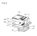
- the junction box in accordance with the present invention includes a PCB unit 100 provided with upper or first and lower or second surfaces 102, 103, on which fuses 110, relays 120, a control and communication unit 130, and connector units 140 and 150 are mounted (see FIGs. 5 and 6 ).
- An upper or first cover 200 covers the upper surface 102 of the PCB unit 100 and exposes the fuses 110 and the first connector unit 140.
- a lower or second cover 300 covers the lower surface 103 of the PCB unit 100 and exposes the second connector unit 150.
- a shielding part 400 shields a region of the lower cover 300 which exposes the second connector unit 150.
- the above junction box includes the PCB unit 100 and the cover units to cover the PCB unit 100. Further, the PCB unit 100 of the junction box is electrically connected to external electronic modules by the first and second connector units 140 and 150. Moreover, the PCB unit 100 of the junction box receives power supplied from the outside, and then distributes the power.
- the junction box is characterized in that the connector units 140 and 150 are disposed on the upper and lower surfaces 102,103 of one board (i.e. a PCB) and the fuses 110, the relays 120, and the control and communication unit 130 are effectively disposed, and thus eliminates use of any additional board (see FIGs. 5 and 6 ). Further, the fuses 110 are disposed on the upper surface 102 of the PCB unit 100, and thus A/S (e.g. repair/replacement) on the fuses 110 is freely performed.
- A/S e.g. repair/replacement
- the PCB unit 100 is covered with the upper cover 200 and the lower cover 300, and thus is protected from external impact.
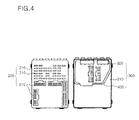
- the upper cover 200 includes an upper or first cover body 210, and fuse exposing grooves or apertures 220 and first connector exposing grooves or apertures 230 provided on the upper cover body 210.
- the upper cover body 210 is formed in the shape of a rectangular box having an opened lower portion.
- the upper cover body 210 is made of an insulating material, such as plastic or rubber, and thus protects the PCB unit 100 from external physical and electrical impacts.
- the fuse exposing grooves 220 to expose a plurality of the fuses 110 mounted on the upper surface 102 of the PCB unit 100 are provided on the upper cover body 210.
- the fuse exposing grooves 220 are formed at positions corresponding to the plurality of the fuses 110.
- the fuses 110 on the PCB unit 100 are exposed to the outside of the upper cover body 210 through the fuse exposing grooves 220. Thereby, the fuses 110 may be easily replaced with new ones. Further, the fuses 110 may be partially exposed to the outside of the upper cover body 210 through the fuse exposing grooves 220.
- the fuse exposing grooves 220 may be omitted, as occasion demands.
- first connector exposing grooves 230 to expose the first connector unit 140 mounted on the upper surface 102 of the PCB unit 100 are provided on the upper cover body 210.
- Connector jacks (or sockets) electrically connected with the first connector unit 140 are inserted into the first connector exposing grooves 230.
- the first connector unit 140 is electrically connected to the outside through the connector jacks inserted into the first connector exposing grooves 230.
- the overall regions or only pin regions of the first connector unit 140 may be exposed through the first connector exposing grooves 230.
- the lower cover 300 corresponding to the above-described the upper cover 200 includes a lower or second cover body 310 and second connector exposing grooves or apertures 320.
- the lower cover body 310 is made of the same material as the upper cover body 210.
- a receipt space is formed by connecting the upper cover body 210 and the lower cover body 310, and the PCB unit 100 is located within the receipt space.
- the second connector exposing grooves 320 to expose the second connector unit 150 mounted on the lower surface of the PCB unit 100 are provided on the lower cover body 310. Connector jacks electrically connected with the second connector unit 150 are inserted into the second connector exposing grooves 320.
- the second connector unit 150 is electrically connected to the outside through the connector jacks inserted into the second connector exposing grooves 320. In the same manner as the first connector exposing grooves 230, the overall regions or only pin regions of the second connector unit 150 may be exposed through the second connector exposing grooves 320.
- the shielding part 400 to shield the second connector exposing grooves 320 is mounted on the lower cover 300 at the second connector exposing grooves 320.
- the shielding part 400 is formed in the shape of a hollow box having an opened upper portion, and a cable box, through which cables pass, and a groove are formed on the upper surface of the shielding part 400.
- the shielding part 400 shields the second connector exposing grooves 320 of the lower cover 300, thereby preventing the second connector exposing grooves 320 from being exposed directly to the outside. Further, the shielding part 400 prevents the second connector unit 150 exposed to the outside through the second connector exposing grooves 320 from being contaminated, and prevents external connection jacks (or plus or sockets) from being easily separated from the second connector unit 150 of the PCB unit 100.
- the fuses 110, the relays 120, and the control and communication unit 130 are integrally mounted on the PCB unit 100, which is surrounded by the upper cover 200 and the lower cover 300, thereby reducing size of the junction box as well as reducing manufacturing costs of the junction box. Further, the first connector unit 140 and the second connector unit 150 are provided on the upper surface and the lower surface 102,103 of the PCB unit 100, thereby facilitating electrical connection with the outside.
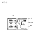
- the PCB unit 100 in accordance with the present invention includes a PCB board or a printed circuit (PC) board 101, a plurality of the fuses 110 mounted on the upper surface 102 of the PCB board 101, a plurality of the relays 120 mounted on the lower surface 103 of the PCB board 101, the control and communication unit 130 (130a and 130b) provided on the upper and lower surfaces 102,103 of the PCB board 101, the first connector unit 140 provided on the upper surface 102 of the PCB board 101, and the second connector unit 150 provided on the lower surface 103 of the PCB board 101.
- PC printed circuit
- the junction box in accordance with the present invention includes elements having a power distribution function and elements having control and communication functions, which are integrated onto one board, thereby reducing manufacturing costs and the number of parts and having reduced size and weight.
- a multilayer board having wire patterns formed on the inside and outer surface thereof is used as the PCB board 101.
- the plural fuses 110 are mounted on the upper surface 102 of the PCB board 101 at one side.
- 2-terminal fuses may be used as the fuses 110.
- Size and standard of the fuses 110 are not limited, and various fuses to distribute power of a vehicle may be used as the fuses 100. Therefore, a mounted part, on which the fuses 110 are mounted, is provided on the PCB board 101.
- the fuses 110 are preferably concentrated upon one side (the left side of FIG. 5 ) of the center of the PCB board 101. Thereby, other parts may be mounted at the other side (the right side of FIG. 5 ).
- the fuses 110 are disposed at the left side of the center of the PCB board 101, and the first connector unit 140 and a first control and communication unit 130a are disposed at the right side of the center of the PCB board 101.
- the center of the PCB board 101 refers to the central line of the PCB board 101.
- the fuses 110 are mounted on the upper surface 102 of the PCB board 101, and thus A/S on the fuses 110 may be easily performed.
- the plural relays 120 are mounted on the lower surface 103 of the PCB board 101.
- the relays 120 may be mounted on the upper surface 102 of the PCB board 101.
- size and standard of the relays 120 are not limited, and various kinds of relay may be used as the relays 120, as occasion demands.
- the junction box in accordance with the present invention includes the control and communication unit 130 having a control function and a communication function of electronic modules.
- control and communication unit 130 is divided into first and second control and communication units 130a and 130b, which are respectively mounted on the upper and lower surfaces 102, 103 of the PCB board 101. If parts (i.e. chips or circuit elements) forming the control and communication unit 130 are formed on one surface, the parts occupy the overall regions of the surface. Therefore, respective elements of the control and communication unit 130 are divided into two units. That is, as shown in FIGs. 5 and 6 , the first control and communication unit 130a is mounted on the upper surface 102 of the PCB board 101, and the second control and communication unit 130b is mounted on the lower surface 103 of the PCB board 101.
- the first control and communication unit 130a is mounted on the upper surface 102 of the PCB board 101 at a region where the fuses 110 are not mounted, thereby being capable of suppressing interference of the first control and communication unit 130a with the fuses 110.
- the second control and communication unit 130b is mounted on the lower surface 103 of the PCB board 101 at a region corresponding to the first control and communication unit 130a, thereby being capable of facilitating electrical connection between the first control and communication unit 130a and the second control and communication unit 130b.
- the second control and communication unit 130b may be mounted on the lower surface 103 of the PCB board 101 at a region corresponding to the fuses 110, thereby being capable of suppressing interference of the second control and communication unit 130b with the fuses 110.
- first and second connector units 140 and 150 to apply power or an electrical signal to the fuses 110, the relays 120, and the control and communication unit 130 mounted on the PCB board 101 or to transmit power or an electrical signal to the outside are mounted on the PCB board 101.
- the first connector unit 140 is formed on the upper surface 102 of the PCB board 101 at a region where the fuses 110 and the first control and communication unit 130a are not mounted, and the first connector unit 140 includes four connectors, as shown in FIG. 5 .
- the second connector unit 150 is formed on the lower surface 103 of the PCB board 101 at a region where the second control and communication unit 130b and the relays 120 are not mounted. Two connectors of the first connector unit 140 are located at the central region of the PCB board 101, and the remaining two connectors are located at the edge of the PCB board 101. That is, the four connectors are disposed in a C shape.
- the second connector unit 150 includes three connectors, as shown in FIG. 6 . Each of the respective connectors is provided with a pin protruded to the outside of the PCB board 101. These connector pins are electrically connected to the fuses 110, the relays 120, and the control and communication unit 130 through wires within the PCB board 101. Two connectors of the second connector unit 150 are located at the edge of the PCB board 101, and the remaining one connector is located at the central region of the PCB board 101. That is, the three connectors are disposed in a T shape.
- the junction box in accordance with the present invention includes the first and second connector units 140 and 150, which are respectively disposed on the upper and lower surfaces 102,103 of the PCB board 101, thereby facilitating electrical connection of the fuses 110, the relays 120, and the control and communication unit 130 mounted on the PCB board 101 with electronic modules of a vehicle. This is achieved by adjusting disposition of the fuses 110, the relays 120, and the control and communication unit 130 on the PCB board 101, as shown in FIGs. 5 and 6 .
- the present invention provides a junction box, in which fuses, relays, and a control and communication unit are mounted on a single board, thereby reducing manufacturing costs of the board, reducing size and weight of the board, and effectively performing communication with external electronic modules.
Landscapes
- Engineering & Computer Science (AREA)
- Mechanical Engineering (AREA)
- Architecture (AREA)
- Civil Engineering (AREA)
- Structural Engineering (AREA)
- Microelectronics & Electronic Packaging (AREA)
- Connection Or Junction Boxes (AREA)
Applications Claiming Priority (1)
| Application Number | Priority Date | Filing Date | Title |
|---|---|---|---|
| KR1020080119210A KR101023885B1 (ko) | 2008-11-27 | 2008-11-27 | 차량용 졍션 박스 |
Publications (2)
| Publication Number | Publication Date |
|---|---|
| EP2192006A1 true EP2192006A1 (fr) | 2010-06-02 |
| EP2192006B1 EP2192006B1 (fr) | 2017-07-26 |
Family
ID=41683006
Family Applications (1)
| Application Number | Title | Priority Date | Filing Date |
|---|---|---|---|
| EP09177176.6A Not-in-force EP2192006B1 (fr) | 2008-11-27 | 2009-11-26 | Boîte de raccordement pour véhicule |
Country Status (4)
| Country | Link |
|---|---|
| US (1) | US8348679B2 (fr) |
| EP (1) | EP2192006B1 (fr) |
| KR (1) | KR101023885B1 (fr) |
| CN (1) | CN101902022B (fr) |
Cited By (1)
| Publication number | Priority date | Publication date | Assignee | Title |
|---|---|---|---|---|
| EP2826674A3 (fr) * | 2013-07-15 | 2015-06-17 | Delphi Technologies, Inc. | Centre de distribution électrique pour un véhicule |
Families Citing this family (12)
| Publication number | Priority date | Publication date | Assignee | Title |
|---|---|---|---|---|
| CN102456999A (zh) * | 2010-10-26 | 2012-05-16 | 泰科电子(上海)有限公司 | 电连接器、电源分配系统以及电源分配方法 |
| KR101857285B1 (ko) * | 2011-07-12 | 2018-05-14 | 타이코에이엠피 주식회사 | 하이브리드 자동차용 전원연결박스 |
| KR101360099B1 (ko) * | 2012-07-05 | 2014-02-12 | 영화테크(주) | 파샬 타입 차량용 전원연결박스 |
| JP6349158B2 (ja) * | 2014-06-06 | 2018-06-27 | 矢崎総業株式会社 | 電気接続箱 |
| US9905985B2 (en) | 2015-06-16 | 2018-02-27 | Lear Corporation | Optimized high current connector pattern for PDB |
| KR102485328B1 (ko) | 2016-12-09 | 2023-01-06 | 현대자동차주식회사 | 전기 자동차의 충전 제어 장치 |
| KR102120354B1 (ko) * | 2018-09-13 | 2020-06-08 | 영화테크(주) | 정션박스 |
| JP6871230B2 (ja) * | 2018-12-28 | 2021-05-12 | 矢崎総業株式会社 | 電気接続箱 |
| DE202020105589U1 (de) * | 2020-09-30 | 2022-01-11 | Tridonic Gmbh & Co Kg | LED-Treiber mit abgesetzter Schmelzsicherung |
| CN115703366B (zh) * | 2021-08-04 | 2025-09-09 | 比亚迪股份有限公司 | 集成控制器、电驱动总成和车辆 |
| DE102021126411A1 (de) * | 2021-10-12 | 2023-04-13 | Bpw Bergische Achsen Kommanditgesellschaft | Elektrisch angetriebenes Nutzfahrzeug, sowie Hochvoltantriebssystem für ein Nutzfahrzeug |
| KR102803609B1 (ko) * | 2023-07-24 | 2025-05-08 | 영화테크(주) | 차량용 전원분배유닛의 전자식 퓨즈 장치 |
Citations (5)
| Publication number | Priority date | Publication date | Assignee | Title |
|---|---|---|---|---|
| US5011417A (en) * | 1989-06-09 | 1991-04-30 | Yazaki Corporation | Structure of connection between bus bar and press-connecting branch terminal in electric connection box |
| EP0700133A2 (fr) | 1994-08-31 | 1996-03-06 | Sumitomo Wiring Systems, Ltd. | Boîte de raccordement électrique |
| EP1179453A2 (fr) * | 2000-08-09 | 2002-02-13 | Sumitomo Wiring Systems, Ltd. | Boíte de connection |
| EP1209036A2 (fr) * | 2000-11-28 | 2002-05-29 | Sumitomo Wiring Systems, Ltd. | Boite de jonction électrique pour un véhicule |
| US20030030996A1 (en) * | 2001-07-23 | 2003-02-13 | Kaori Shiina | Electrical connection box |
Family Cites Families (12)
| Publication number | Priority date | Publication date | Assignee | Title |
|---|---|---|---|---|
| JP3693137B2 (ja) | 1996-08-05 | 2005-09-07 | 矢崎総業株式会社 | 電気接続箱の接続構造及び接続方法 |
| JP2999708B2 (ja) * | 1996-02-28 | 2000-01-17 | 株式会社ハーネス総合技術研究所 | 電気接続箱 |
| EP1145914B1 (fr) | 2000-04-13 | 2006-05-17 | Sumitomo Wiring Systems, Ltd. | Boîtier de raccordement électrique |
| US20030022535A1 (en) * | 2001-06-25 | 2003-01-30 | Thomas Schoepf | Fuse and relay box in a motor vehicle |
| KR100435914B1 (ko) | 2001-11-20 | 2004-06-12 | 타이코에이엠피 주식회사 | 정션박스 및 인쇄회로기판의 납땜방법 |
| KR100451925B1 (ko) | 2001-12-13 | 2004-10-08 | 타이코에이엠피 주식회사 | 집적 회로 모듈 |
| KR100516513B1 (ko) * | 2004-02-19 | 2005-09-26 | 타이코에이엠피 주식회사 | 차량용 정션박스 및 그 조립방법 |
| JP3888368B2 (ja) | 2004-07-13 | 2007-02-28 | 住友電装株式会社 | 電気接続箱 |
| JP5037235B2 (ja) * | 2006-11-16 | 2012-09-26 | 株式会社オートネットワーク技術研究所 | 電気接続箱 |
| JP4453726B2 (ja) * | 2007-07-20 | 2010-04-21 | 住友電装株式会社 | 車載用のジャンクションボックス |
| JP5077190B2 (ja) | 2008-10-28 | 2012-11-21 | 住友電装株式会社 | プリント基板 |
| US7931479B1 (en) | 2009-11-17 | 2011-04-26 | Delphi Technologies, Inc. | Bussed electrical center with combination electrical and mechanical connection |
-
2008
- 2008-11-27 KR KR1020080119210A patent/KR101023885B1/ko active Active
-
2009
- 2009-11-24 US US12/625,074 patent/US8348679B2/en not_active Expired - Fee Related
- 2009-11-26 EP EP09177176.6A patent/EP2192006B1/fr not_active Not-in-force
- 2009-11-27 CN CN200910246132.1A patent/CN101902022B/zh active Active
Patent Citations (5)
| Publication number | Priority date | Publication date | Assignee | Title |
|---|---|---|---|---|
| US5011417A (en) * | 1989-06-09 | 1991-04-30 | Yazaki Corporation | Structure of connection between bus bar and press-connecting branch terminal in electric connection box |
| EP0700133A2 (fr) | 1994-08-31 | 1996-03-06 | Sumitomo Wiring Systems, Ltd. | Boîte de raccordement électrique |
| EP1179453A2 (fr) * | 2000-08-09 | 2002-02-13 | Sumitomo Wiring Systems, Ltd. | Boíte de connection |
| EP1209036A2 (fr) * | 2000-11-28 | 2002-05-29 | Sumitomo Wiring Systems, Ltd. | Boite de jonction électrique pour un véhicule |
| US20030030996A1 (en) * | 2001-07-23 | 2003-02-13 | Kaori Shiina | Electrical connection box |
Cited By (1)
| Publication number | Priority date | Publication date | Assignee | Title |
|---|---|---|---|---|
| EP2826674A3 (fr) * | 2013-07-15 | 2015-06-17 | Delphi Technologies, Inc. | Centre de distribution électrique pour un véhicule |
Also Published As
| Publication number | Publication date |
|---|---|
| KR20100060576A (ko) | 2010-06-07 |
| EP2192006B1 (fr) | 2017-07-26 |
| CN101902022A (zh) | 2010-12-01 |
| CN101902022B (zh) | 2014-05-28 |
| KR101023885B1 (ko) | 2011-03-22 |
| US8348679B2 (en) | 2013-01-08 |
| US20100130033A1 (en) | 2010-05-27 |
Similar Documents
| Publication | Publication Date | Title |
|---|---|---|
| EP2192006B1 (fr) | Boîte de raccordement pour véhicule | |
| US8043112B2 (en) | Jack connector assembly having circuity components integrated for providing POE-functionality | |
| CN1794526B (zh) | 配电箱及其组装方法 | |
| KR20110119696A (ko) | 다층 pcb를 갖는 원격통신 잭 | |
| US7442052B2 (en) | Junction block having improved support for its printed circuit board | |
| WO2018159352A1 (fr) | Module de connexion | |
| US7563111B2 (en) | Board connector | |
| KR200358267Y1 (ko) | 차량용 통합 전자 모듈의 구조 | |
| US20200113070A1 (en) | Wire Harness | |
| JP2018093685A (ja) | 電気接続箱、及び、ワイヤハーネス | |
| US20030147221A1 (en) | Integral high current stamped metal circuit for printed circuit board bussed electrical center | |
| JP7701254B2 (ja) | 接続体及びハーネス | |
| EP4210180B1 (fr) | Ensemble connecteur et son procédé de fabrication et dispositif électronique | |
| KR101601299B1 (ko) | 자동차용 정션박스 | |
| US5755580A (en) | Universal cable connecting box for vehicles | |
| US10988090B2 (en) | Wire harness system | |
| US20070277999A1 (en) | Circuit board and electrical connection box having the same | |
| KR100654708B1 (ko) | 차량용 통합 전자 모듈의 구조 | |
| EP2083486B1 (fr) | Protection électromagnétique pour agencement de connecteur | |
| JP2007317990A (ja) | フレキシブルプリント配線板 | |
| KR200388110Y1 (ko) | 정션 박스 | |
| JPH0688076U (ja) | 入出力用コネクタ | |
| JP2024041119A (ja) | 電源ボックス | |
| KR19980033187U (ko) | 휴즈 및 릴레이 박스 | |
| JP2024132936A (ja) | ディジタル保護リレー及びアナログ入力回路基板 |
Legal Events
| Date | Code | Title | Description |
|---|---|---|---|
| PUAI | Public reference made under article 153(3) epc to a published international application that has entered the european phase |
Free format text: ORIGINAL CODE: 0009012 |
|
| AK | Designated contracting states |
Kind code of ref document: A1 Designated state(s): AT BE BG CH CY CZ DE DK EE ES FI FR GB GR HR HU IE IS IT LI LT LU LV MC MK MT NL NO PL PT RO SE SI SK SM TR |
|
| AX | Request for extension of the european patent |
Extension state: AL BA RS |
|
| 17P | Request for examination filed |
Effective date: 20101021 |
|
| 17Q | First examination report despatched |
Effective date: 20101223 |
|
| GRAP | Despatch of communication of intention to grant a patent |
Free format text: ORIGINAL CODE: EPIDOSNIGR1 |
|
| INTG | Intention to grant announced |
Effective date: 20170223 |
|
| RIN1 | Information on inventor provided before grant (corrected) |
Inventor name: HO, LEE JOON Inventor name: KYU, LEE JONG |
|
| GRAS | Grant fee paid |
Free format text: ORIGINAL CODE: EPIDOSNIGR3 |
|
| GRAA | (expected) grant |
Free format text: ORIGINAL CODE: 0009210 |
|
| RAP1 | Party data changed (applicant data changed or rights of an application transferred) |
Owner name: TYCO ELECTRONICS AMP KOREA CO., LTD. |
|
| AK | Designated contracting states |
Kind code of ref document: B1 Designated state(s): AT BE BG CH CY CZ DE DK EE ES FI FR GB GR HR HU IE IS IT LI LT LU LV MC MK MT NL NO PL PT RO SE SI SK SM TR |
|
| REG | Reference to a national code |
Ref country code: GB Ref legal event code: FG4D |
|
| REG | Reference to a national code |
Ref country code: CH Ref legal event code: EP |
|
| REG | Reference to a national code |
Ref country code: AT Ref legal event code: REF Ref document number: 912080 Country of ref document: AT Kind code of ref document: T Effective date: 20170815 |
|
| REG | Reference to a national code |
Ref country code: IE Ref legal event code: FG4D |
|
| REG | Reference to a national code |
Ref country code: DE Ref legal event code: R096 Ref document number: 602009047318 Country of ref document: DE |
|
| REG | Reference to a national code |
Ref country code: FR Ref legal event code: PLFP Year of fee payment: 9 |
|
| REG | Reference to a national code |
Ref country code: NL Ref legal event code: MP Effective date: 20170726 |
|
| REG | Reference to a national code |
Ref country code: LT Ref legal event code: MG4D |
|
| REG | Reference to a national code |
Ref country code: AT Ref legal event code: MK05 Ref document number: 912080 Country of ref document: AT Kind code of ref document: T Effective date: 20170726 |
|
| PG25 | Lapsed in a contracting state [announced via postgrant information from national office to epo] |
Ref country code: AT Free format text: LAPSE BECAUSE OF FAILURE TO SUBMIT A TRANSLATION OF THE DESCRIPTION OR TO PAY THE FEE WITHIN THE PRESCRIBED TIME-LIMIT Effective date: 20170726 Ref country code: FI Free format text: LAPSE BECAUSE OF FAILURE TO SUBMIT A TRANSLATION OF THE DESCRIPTION OR TO PAY THE FEE WITHIN THE PRESCRIBED TIME-LIMIT Effective date: 20170726 Ref country code: NO Free format text: LAPSE BECAUSE OF FAILURE TO SUBMIT A TRANSLATION OF THE DESCRIPTION OR TO PAY THE FEE WITHIN THE PRESCRIBED TIME-LIMIT Effective date: 20171026 Ref country code: HR Free format text: LAPSE BECAUSE OF FAILURE TO SUBMIT A TRANSLATION OF THE DESCRIPTION OR TO PAY THE FEE WITHIN THE PRESCRIBED TIME-LIMIT Effective date: 20170726 Ref country code: LT Free format text: LAPSE BECAUSE OF FAILURE TO SUBMIT A TRANSLATION OF THE DESCRIPTION OR TO PAY THE FEE WITHIN THE PRESCRIBED TIME-LIMIT Effective date: 20170726 Ref country code: NL Free format text: LAPSE BECAUSE OF FAILURE TO SUBMIT A TRANSLATION OF THE DESCRIPTION OR TO PAY THE FEE WITHIN THE PRESCRIBED TIME-LIMIT Effective date: 20170726 Ref country code: SE Free format text: LAPSE BECAUSE OF FAILURE TO SUBMIT A TRANSLATION OF THE DESCRIPTION OR TO PAY THE FEE WITHIN THE PRESCRIBED TIME-LIMIT Effective date: 20170726 |
|
| PG25 | Lapsed in a contracting state [announced via postgrant information from national office to epo] |
Ref country code: PL Free format text: LAPSE BECAUSE OF FAILURE TO SUBMIT A TRANSLATION OF THE DESCRIPTION OR TO PAY THE FEE WITHIN THE PRESCRIBED TIME-LIMIT Effective date: 20170726 Ref country code: GR Free format text: LAPSE BECAUSE OF FAILURE TO SUBMIT A TRANSLATION OF THE DESCRIPTION OR TO PAY THE FEE WITHIN THE PRESCRIBED TIME-LIMIT Effective date: 20171027 Ref country code: LV Free format text: LAPSE BECAUSE OF FAILURE TO SUBMIT A TRANSLATION OF THE DESCRIPTION OR TO PAY THE FEE WITHIN THE PRESCRIBED TIME-LIMIT Effective date: 20170726 Ref country code: BG Free format text: LAPSE BECAUSE OF FAILURE TO SUBMIT A TRANSLATION OF THE DESCRIPTION OR TO PAY THE FEE WITHIN THE PRESCRIBED TIME-LIMIT Effective date: 20171026 Ref country code: ES Free format text: LAPSE BECAUSE OF FAILURE TO SUBMIT A TRANSLATION OF THE DESCRIPTION OR TO PAY THE FEE WITHIN THE PRESCRIBED TIME-LIMIT Effective date: 20170726 Ref country code: IS Free format text: LAPSE BECAUSE OF FAILURE TO SUBMIT A TRANSLATION OF THE DESCRIPTION OR TO PAY THE FEE WITHIN THE PRESCRIBED TIME-LIMIT Effective date: 20171126 |
|
| PG25 | Lapsed in a contracting state [announced via postgrant information from national office to epo] |
Ref country code: DK Free format text: LAPSE BECAUSE OF FAILURE TO SUBMIT A TRANSLATION OF THE DESCRIPTION OR TO PAY THE FEE WITHIN THE PRESCRIBED TIME-LIMIT Effective date: 20170726 Ref country code: CZ Free format text: LAPSE BECAUSE OF FAILURE TO SUBMIT A TRANSLATION OF THE DESCRIPTION OR TO PAY THE FEE WITHIN THE PRESCRIBED TIME-LIMIT Effective date: 20170726 Ref country code: RO Free format text: LAPSE BECAUSE OF FAILURE TO SUBMIT A TRANSLATION OF THE DESCRIPTION OR TO PAY THE FEE WITHIN THE PRESCRIBED TIME-LIMIT Effective date: 20170726 |
|
| REG | Reference to a national code |
Ref country code: DE Ref legal event code: R097 Ref document number: 602009047318 Country of ref document: DE |
|
| PG25 | Lapsed in a contracting state [announced via postgrant information from national office to epo] |
Ref country code: EE Free format text: LAPSE BECAUSE OF FAILURE TO SUBMIT A TRANSLATION OF THE DESCRIPTION OR TO PAY THE FEE WITHIN THE PRESCRIBED TIME-LIMIT Effective date: 20170726 Ref country code: IT Free format text: LAPSE BECAUSE OF FAILURE TO SUBMIT A TRANSLATION OF THE DESCRIPTION OR TO PAY THE FEE WITHIN THE PRESCRIBED TIME-LIMIT Effective date: 20170726 Ref country code: SK Free format text: LAPSE BECAUSE OF FAILURE TO SUBMIT A TRANSLATION OF THE DESCRIPTION OR TO PAY THE FEE WITHIN THE PRESCRIBED TIME-LIMIT Effective date: 20170726 Ref country code: SM Free format text: LAPSE BECAUSE OF FAILURE TO SUBMIT A TRANSLATION OF THE DESCRIPTION OR TO PAY THE FEE WITHIN THE PRESCRIBED TIME-LIMIT Effective date: 20170726 |
|
| PLBE | No opposition filed within time limit |
Free format text: ORIGINAL CODE: 0009261 |
|
| STAA | Information on the status of an ep patent application or granted ep patent |
Free format text: STATUS: NO OPPOSITION FILED WITHIN TIME LIMIT |
|
| PG25 | Lapsed in a contracting state [announced via postgrant information from national office to epo] |
Ref country code: MC Free format text: LAPSE BECAUSE OF FAILURE TO SUBMIT A TRANSLATION OF THE DESCRIPTION OR TO PAY THE FEE WITHIN THE PRESCRIBED TIME-LIMIT Effective date: 20170726 |
|
| 26N | No opposition filed |
Effective date: 20180430 |
|
| GBPC | Gb: european patent ceased through non-payment of renewal fee |
Effective date: 20171126 |
|
| PG25 | Lapsed in a contracting state [announced via postgrant information from national office to epo] |
Ref country code: LI Free format text: LAPSE BECAUSE OF NON-PAYMENT OF DUE FEES Effective date: 20171130 Ref country code: CH Free format text: LAPSE BECAUSE OF NON-PAYMENT OF DUE FEES Effective date: 20171130 |
|
| PG25 | Lapsed in a contracting state [announced via postgrant information from national office to epo] |
Ref country code: LU Free format text: LAPSE BECAUSE OF NON-PAYMENT OF DUE FEES Effective date: 20171126 Ref country code: SI Free format text: LAPSE BECAUSE OF FAILURE TO SUBMIT A TRANSLATION OF THE DESCRIPTION OR TO PAY THE FEE WITHIN THE PRESCRIBED TIME-LIMIT Effective date: 20170726 |
|
| REG | Reference to a national code |
Ref country code: BE Ref legal event code: MM Effective date: 20171130 |
|
| REG | Reference to a national code |
Ref country code: IE Ref legal event code: MM4A |
|
| PG25 | Lapsed in a contracting state [announced via postgrant information from national office to epo] |
Ref country code: MT Free format text: LAPSE BECAUSE OF NON-PAYMENT OF DUE FEES Effective date: 20171126 |
|
| REG | Reference to a national code |
Ref country code: FR Ref legal event code: PLFP Year of fee payment: 10 |
|
| PG25 | Lapsed in a contracting state [announced via postgrant information from national office to epo] |
Ref country code: IE Free format text: LAPSE BECAUSE OF NON-PAYMENT OF DUE FEES Effective date: 20171126 |
|
| PG25 | Lapsed in a contracting state [announced via postgrant information from national office to epo] |
Ref country code: BE Free format text: LAPSE BECAUSE OF NON-PAYMENT OF DUE FEES Effective date: 20171130 Ref country code: GB Free format text: LAPSE BECAUSE OF NON-PAYMENT OF DUE FEES Effective date: 20171126 |
|
| PGFP | Annual fee paid to national office [announced via postgrant information from national office to epo] |
Ref country code: DE Payment date: 20181113 Year of fee payment: 10 |
|
| PGFP | Annual fee paid to national office [announced via postgrant information from national office to epo] |
Ref country code: FR Payment date: 20181011 Year of fee payment: 10 |
|
| PG25 | Lapsed in a contracting state [announced via postgrant information from national office to epo] |
Ref country code: HU Free format text: LAPSE BECAUSE OF FAILURE TO SUBMIT A TRANSLATION OF THE DESCRIPTION OR TO PAY THE FEE WITHIN THE PRESCRIBED TIME-LIMIT; INVALID AB INITIO Effective date: 20091126 |
|
| PG25 | Lapsed in a contracting state [announced via postgrant information from national office to epo] |
Ref country code: CY Free format text: LAPSE BECAUSE OF NON-PAYMENT OF DUE FEES Effective date: 20170726 |
|
| PG25 | Lapsed in a contracting state [announced via postgrant information from national office to epo] |
Ref country code: MK Free format text: LAPSE BECAUSE OF FAILURE TO SUBMIT A TRANSLATION OF THE DESCRIPTION OR TO PAY THE FEE WITHIN THE PRESCRIBED TIME-LIMIT Effective date: 20170726 |
|
| PG25 | Lapsed in a contracting state [announced via postgrant information from national office to epo] |
Ref country code: TR Free format text: LAPSE BECAUSE OF FAILURE TO SUBMIT A TRANSLATION OF THE DESCRIPTION OR TO PAY THE FEE WITHIN THE PRESCRIBED TIME-LIMIT Effective date: 20170726 |
|
| PG25 | Lapsed in a contracting state [announced via postgrant information from national office to epo] |
Ref country code: PT Free format text: LAPSE BECAUSE OF FAILURE TO SUBMIT A TRANSLATION OF THE DESCRIPTION OR TO PAY THE FEE WITHIN THE PRESCRIBED TIME-LIMIT Effective date: 20170726 |
|
| REG | Reference to a national code |
Ref country code: DE Ref legal event code: R119 Ref document number: 602009047318 Country of ref document: DE |
|
| PG25 | Lapsed in a contracting state [announced via postgrant information from national office to epo] |
Ref country code: FR Free format text: LAPSE BECAUSE OF NON-PAYMENT OF DUE FEES Effective date: 20191130 Ref country code: DE Free format text: LAPSE BECAUSE OF NON-PAYMENT OF DUE FEES Effective date: 20200603 |