EP2192765A1 - Élément d'imagerie à semi-conducteurs et son procédé d'excitation - Google Patents
Élément d'imagerie à semi-conducteurs et son procédé d'excitation Download PDFInfo
- Publication number
- EP2192765A1 EP2192765A1 EP08829005A EP08829005A EP2192765A1 EP 2192765 A1 EP2192765 A1 EP 2192765A1 EP 08829005 A EP08829005 A EP 08829005A EP 08829005 A EP08829005 A EP 08829005A EP 2192765 A1 EP2192765 A1 EP 2192765A1
- Authority
- EP
- European Patent Office
- Prior art keywords
- pixel
- pixels
- signals
- memory
- signal
- Prior art date
- Legal status (The legal status is an assumption and is not a legal conclusion. Google has not performed a legal analysis and makes no representation as to the accuracy of the status listed.)
- Granted
Links
Images






Classifications
-
- H—ELECTRICITY
- H04—ELECTRIC COMMUNICATION TECHNIQUE
- H04N—PICTORIAL COMMUNICATION, e.g. TELEVISION
- H04N25/00—Circuitry of solid-state image sensors [SSIS]; Control thereof
- H04N25/50—Control of the SSIS exposure
- H04N25/57—Control of the dynamic range
- H04N25/58—Control of the dynamic range involving two or more exposures
- H04N25/587—Control of the dynamic range involving two or more exposures acquired sequentially, e.g. using the combination of odd and even image fields
-
- H—ELECTRICITY
- H04—ELECTRIC COMMUNICATION TECHNIQUE
- H04N—PICTORIAL COMMUNICATION, e.g. TELEVISION
- H04N25/00—Circuitry of solid-state image sensors [SSIS]; Control thereof
-
- H—ELECTRICITY
- H04—ELECTRIC COMMUNICATION TECHNIQUE
- H04N—PICTORIAL COMMUNICATION, e.g. TELEVISION
- H04N25/00—Circuitry of solid-state image sensors [SSIS]; Control thereof
- H04N25/50—Control of the SSIS exposure
- H04N25/57—Control of the dynamic range
- H04N25/59—Control of the dynamic range by controlling the amount of charge storable in the pixel, e.g. modification of the charge conversion ratio of the floating node capacitance
-
- H—ELECTRICITY
- H04—ELECTRIC COMMUNICATION TECHNIQUE
- H04N—PICTORIAL COMMUNICATION, e.g. TELEVISION
- H04N25/00—Circuitry of solid-state image sensors [SSIS]; Control thereof
- H04N25/60—Noise processing, e.g. detecting, correcting, reducing or removing noise
- H04N25/616—Noise processing, e.g. detecting, correcting, reducing or removing noise involving a correlated sampling function, e.g. correlated double sampling [CDS] or triple sampling
-
- H—ELECTRICITY
- H04—ELECTRIC COMMUNICATION TECHNIQUE
- H04N—PICTORIAL COMMUNICATION, e.g. TELEVISION
- H04N25/00—Circuitry of solid-state image sensors [SSIS]; Control thereof
- H04N25/70—SSIS architectures; Circuits associated therewith
- H04N25/76—Addressed sensors, e.g. MOS or CMOS sensors
- H04N25/767—Horizontal readout lines, multiplexers or registers
-
- H—ELECTRICITY
- H04—ELECTRIC COMMUNICATION TECHNIQUE
- H04N—PICTORIAL COMMUNICATION, e.g. TELEVISION
- H04N25/00—Circuitry of solid-state image sensors [SSIS]; Control thereof
- H04N25/70—SSIS architectures; Circuits associated therewith
- H04N25/76—Addressed sensors, e.g. MOS or CMOS sensors
- H04N25/77—Pixel circuitry, e.g. memories, A/D converters, pixel amplifiers, shared circuits or shared components
-
- H—ELECTRICITY
- H04—ELECTRIC COMMUNICATION TECHNIQUE
- H04N—PICTORIAL COMMUNICATION, e.g. TELEVISION
- H04N25/00—Circuitry of solid-state image sensors [SSIS]; Control thereof
- H04N25/70—SSIS architectures; Circuits associated therewith
- H04N25/76—Addressed sensors, e.g. MOS or CMOS sensors
- H04N25/77—Pixel circuitry, e.g. memories, A/D converters, pixel amplifiers, shared circuits or shared components
- H04N25/771—Pixel circuitry, e.g. memories, A/D converters, pixel amplifiers, shared circuits or shared components comprising storage means other than floating diffusion
-
- H—ELECTRICITY
- H04—ELECTRIC COMMUNICATION TECHNIQUE
- H04N—PICTORIAL COMMUNICATION, e.g. TELEVISION
- H04N25/00—Circuitry of solid-state image sensors [SSIS]; Control thereof
- H04N25/70—SSIS architectures; Circuits associated therewith
- H04N25/76—Addressed sensors, e.g. MOS or CMOS sensors
- H04N25/78—Readout circuits for addressed sensors, e.g. output amplifiers or A/D converters
Definitions
- Patent Document 1 One example off this type of solid-state images sensor is disclosed in Patent Document 1 and other documents, which is referred to as an in-situ storage image sensor (IS-CCD).
- An outline of this image sensor is as follows: A storage COD, which also serves for the transfer of a specified number off recorded images (frames), is provided for each photodiode as a photo-receiver. During an imaging operation, pixel signals resulting from photoelectric conversion by the photodiode are sequentially transferred to the storage CCD. After the imaging operation, is completed, the pixels signals corresponding to the specified number of record frames stored in the storage CCD are collectively read, and the images corresponding to the specified number of record frames are reproduced outside the image sensor.
- the system In the aforementioned high-speed imaging, it is important to perform the imaging in synchronization with the timing of the occurrence of a phenomenon under observation. This is achieved by a control process in which the imaging action is initiated or discontinued in response to an externally given trigger signal.
- the system normally includes another sensor, such as a contact sensor, position sensor, vibration sensor or pressure sensor.
- another sensor such as a contact sensor, position sensor, vibration sensor or pressure sensor.
- it is often difficult in some situations to obtain appropriate trigger signals by this method as in the case where the sensor cannot be easily placed close to the object, where the imaging action must capture a spontaneous change in the object under observation, or where the target of imaging is a micro-sized object under a microscope.
- the present invention has been developed in view of the previously described problems. Its first objective is to provide a solid-state image sensor capable of both an ultrahigh-speed imaging mode that has a limitation on the number of record frames and another imaging mode that is rather slow but has no limitation on the number of record frames, and a method for driving this image sensor.
- the second objective of the present invention is to provide a solid-state image sensor suitable for capturing a change in an object within a series of continuously taken images or an occurrence of a phenomenon under observation to correctly control the initiation, discontinuation and other actions of high-speed imaging, and a method for driving this image sensor.
- the present invention aimed at solving the aforementioned problems provides a drive method for a solid-state image sensor having a plurality of pixels arranged in a two-dimensional array; each pixel including at least a photoelectric conversion element for receiving light and producing photocharges, a transfer element for transferring the photocharges produced by the photoelectric conversion element to a detection node, and a buffer element for sending a signal from the detection node to a pixel output line, the pixel output, line being independently provided for each pixel, one or more memory sections being provided for each pixel; the memory section being used to hold a signal extracted from each pixel through the pixel output line; and the method being characterized in that at least one of the following modes is performed:
- a solid-state image sensor according to the present invention aimed at solving the previously described problems is a solid-state image sensor for implementing the previously described drive method, which is characterized by including:
- the photoelectric conversion element included in each pixel may be a photodiode
- the detection node may be a floating diffusion (floating region)
- the transfer element may be a transistor (MOS transistor)
- the buffer element may be a source follower amplifier composed off a plurality off transistors.
- the memory section (and memory unit) may be a combination of a capacitor and a switch such as a transistor.
- the second drive mode of' the solid-state image sensor and its drive method according to the present invention it is possible to perform continuous imaging at extremely high-speeds over a plurality off frames since there is no need to interrupt the contiguous imaging operation to read the signals (pixel signals) obtained during the imaging operation to the outside of the sensor.
- the transfer of signals from each pixel to the memory section car be completed within an extremely short period of time. Therefore, the period of time required for taking one frame of image is mostly determined by the period of time required for receiving light by the photoelectric conversion element and storing the photocharges into the detection node oar the like.
- the number off frames from which images can be read to the outside of the sensor at a later time is limited by the number of memory sections provided for each pixel. That is, if there are one hundred memory sections for each pixel, it is possible to obtain one hundred frames of continuous images.
- the drive speed cannot be as high as in the second drive mode.
- the number of image frames is not limited by the number of memory sections provided for each pixel.
- the operations according to the two drive modes can be linked to each other; for example, it is possible to initially operate the solid-state Image sensor in the first drive mode and then switch to the second drive mode in response to a trigger signal, which is generated when an occurrence of a phenomenon of interest or a change in an object has been recognized based on the pixel signals produced by the solid-state image sensor.
- a trigger signal which is generated when an occurrence of a phenomenon of interest or a change in an object has been recognized based on the pixel signals produced by the solid-state image sensor.
- the noise signal includes a fixed pattern noise, such as a change in the threshold voltage of a transistor included in a buffer element, and a random noise that occurs in a detection node, such as a floating diffusion. These noise components are also superposed on the signal corresponding to the photocharges.
- a fixed pattern noise such as a change in the threshold voltage of a transistor included in a buffer element
- a random noise that occurs in a detection node, such as a floating diffusion.
- An example of the aforementioned charge storage element is a capacitor having a double polysilicon structure or stack structure.
- the detection node such as a floating diffusion.
- the detection node may be saturated when a large amount of photocharges are produced by strong incident, light.
- the photocharges that have been generated in the photoelectric conversion element and overflowed, for example, from the detection node are stored in the photocharge storage element. Therefore, even when a large amount of photocharges are produced by strong incident light, the photocharges will not be wasted but can be reflected in the signals, Conversely, when the incident light is weak and the amount of resultant photocharges is accordingly small, only the signals stored in the low-capacitance detection node are used. Thus, the dynamic range is widened by the aforementioned variation of the present invention.
- a signal-holding operation is performed in which the plurality of memory sections are cyclically used so that, after the signals are held in all the memory sections corresponding to the pixels, the memory section holding the oldest signal is reset to hold a new signal, and the operation of holding a new signal in the memory section is halted in response to a halt instruction. It is recommendable that the actual halting of the operation of holding a new signal in the memory section can be appropriately delayed from the point in time of the halt instruction, in which case it is preferable that the delay time or the number of frames can be externally set.
- this method it is possible, in the second drive mode, to repeat a high-speed imaging operation without reading pixel signals to the outside of the sensor and, for example, obtain images before and after a point in time where a trigger signal has been externally provided. Therefore, at the moment of occurrence of a certain situation, such as a change in an object, it is possible to obtain images not only after that moment but also before that moment.
- the first drive mode and the second drive mode it is possible to detect a specific event based on the image information derived from a portion or entirety of one or more frames of images produced by performing the first drive mode, and to perform the second drive mode according to the detection result. This can be interpreted as the trigger signal being generated by the detection of a specific event.
- the solid-state image sensor and its drive method according to the present invention it is also possible to alternately perform the first drive mode and the second drive mode an arbitrary number of times or at arbitrary intervals of time.
- the memory sections still hold the signals obtained in the preceding cycle of the second drive mode. By reading these signals, it is possible to obtain images that temporally precede the detection of the change in the object.
- a portion of the memory sections for the second drive mode can be utilized during an operation in the first drive mode.
- the memory sections available can be entirety used in the second drive mode, which accordingly increases the possible number of frames for continuous imaging.
- the memory sections for the first drive mode and those for the second drive mode are independent of each other.
- the output 42 of the low-voltage side transistor 41 in the second stage of the source follower amplifier 43 is connected to one of the 132 pixels output lines 14 (i.e. the pixel output line denoted by numeral 141 in Fig. 5 ) provided in the aforementioned wiring area 13.
- Such a pixel output line 141 is provided for every pixel 10, i.e. independently for each pixel 10. Therefore, the present solid-state image sensor has as many pixel output lines as the number of pixels, i.e. 84480.
- the source follower amplifier 43 functions as a current buffer for driving the pixel output line 141 at high speeds.
- each pixel output line 141 extends from the pixel area 2a to the memory area 3a and hence acts as a considerably large capacitive load.
- Driving such an element at high speeds requires a large-sized transistor through which high currents can be passed.
- the floating diffusion 33 for converting photocharges to voltage should preferably have the smallest possible capacitance.
- the parasitic capacitance of the gate terminal of the transistor connected to the floating diffusion 33 causes an effective increase in the capacitance of the floating diffusion 33.
- this transistor 37 should preferably be a small-sized transistor with a small gate input capacitance.
- the source follower amplifier 43 in the present embodiment has a two-stage configuration, where a small-sized transistor is used as the transistor 37 in the first stage to reduce the input gate capacitance while large-seized transistors are used as the second-stage transistors 40 and 41 to ensure a high output current.
- the selection transistor 38 in the first stage of the source follower amplifier 43 is not essential for the basic operation. However, when the second-stage selection transistor 41 is off, this selection transistor 38 can be simultaneously turned off to block the flow of current from the current source 39 into the transistor 37 and thereby suppress the consumption of electric power.
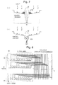
- Fig. 6 is a schematic plan view showing the layout of the photoelectric conversion area 11 in one pixel 10
- Fig. 7 is a schematic potential diagram at the vertical section indicated by the arrowed line A-A' in Fig. 6 .
- the photodiode 31 which has a photo-receiving surface that is substantially rectangular when viewed from above, has an embedded photodiode structure, In high-speed imaging, the exposure time is extremely short. Therefore, to ensure appropriate exposure, the photodiode of each pixel 10 needs to have the largest possible photo-receiving surface so that it can receive the largest possible amount of incident light. However, increasing the area of the photo-receiving surface of the photodiode normally causes a problem relating to the time required for the photocharges to reach the floating diffusion, i.e. the detection node, particularly for the photocharges produced in the circumferential portion of the photo-receiving surface.
- the solid-state image sensor of the present embodiment has adopted a special structure, as hereafter described, to improve the charge-transfer speed.
- the present solid-state image sensor has a small-sized floating diffusion 331 located nearly at the center of the photodiode 31, with the ring-shaped gate of the transfer transistor 32 encircling the floating diffusion 331. Placing the floating diffusion 331 at the center of the photodiode 31 in this manner reduces, on average, the moving distance of the photocharges from the circumferential portion of the photodiode 31 to the floating diffusion 331. Accordingly, the photocharges can easily reach the floating diffusion 331 irrespective of where they are generated within the circumferential portion of the photodiode 31.
- the amount (or depth) of injection (doping) of impurities is changed in stages by using a plurality of photomasks to provide a gradient or stepwise change in the amount of doping (or injection depth) of the impurities from the circumference of the photodiode 31 toward its center (i.e. the floating diffusion 331). Therefore, when an appropriate bias voltage is applied to the PN junction of the photodiode 31, a potential gradient that declines from the circumference of the photodiode 31 toward its center is created, as shown in Fig. 7(a) . Due to this intended potential gradient created by a skillfully devised process, a photocharge produced by incident light at a location closer to the circumference of the photodiode 31 is more rapidly accelerated toward the center.
- the provision of the flouting diffusion 331 at the center of the photodiode 31 offers the previously described significant advantages.
- the previous configuration causes the problem that the aperture ratio will decrease if another element, such as a storage capacitor 36 for storing photocharges that have overflowed, is placed close to the floating diffusion 331.
- This problem is avoided in the present embodiment by providing a second floating diffusion 332 as a diffusion layer within the pixel circuit area 12 in addition to the aforementioned floating diffusion 331 which photocharges directly flow into as described previously (this floating diffusion is hereinafter called the first floating diffusion, with a wire 333 made of aluminum or other kinds of metal connecting the first floating diffusion 331 and the second floating diffusion 332 to equalize their potential.
- the first floating diffusion 331 and the second floating diffusion 332 integrally function as a floating diffusion 33 which serves as the detection node for converting electric charge signals into voltage signals.
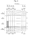
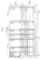
- each of the first and second memory areas 3a and 3b includes memory section units 20 whose number equals the number L of storage frames. These memory section units 20 are arrayed in the extending direction of the 132 pixel output lines 14 which are respectively connected to the 132 pixels 10 vertically arranged within the pixel area 2a or 2b.
- the number L of storage frames, or the number of frames for continuous imaging is 104. Accordingly, 104 pieces of memory section units 20 are vertically arranged to form a column, and 320 copies of this column are arranged horizontally.
- the second memory area 3b also has the same number of memory section units 20.
- Fig. 8 is a schematic diagram showing the internal configuration of one memory section unit 20.
- Each memory section unit 20 includes a total of 132 memory sections 22 forming an array with 12 rows and 11 columns.
- Each memory section 20 is connected to a different pixel output line 141.
- the pixel output lines 141 establish a one-to-one relation between the memory sections 22 and the pixels 10 within the pixel area 2a.
- the 132 memory sections 22 within one memory section unit 20 hold signals received from the 132 pixels forming one column within the pixel area 2a. Therefore, the 320 memory section units 20 forming one horizontal row in Fig. 4 (i.e. the row of memory section units denoted by numeral 21 in Fig.
- each memory section unit 20 all outputs of the 132 memory sections 22 in each memory section unit 20 are connected together to form a single output line 23.
- the horizontally arranged memory section units 20 are divided into groups each consisting of ten neighboring Memory section units 20.
- 32 group of memory section units 20 are horizontally arranged, where the output lines 23 of the ten memory section units 20 in each group are connected together to form a single line.
- the output lines 23 of the vertically arranged 104 memory section units 20 are also connected together to form a single lime.
- a memory section unit block which is a collection of the memory section units 20 sharing the same output line 23, is denoted by numeral 50.
- the configuration described to this point results in 32 output lines 23 extracted from the first memory area 3a and the same number of output lines 23 extracted from the second memory area 3b.
- the signals extracted through these output lines 23 are denoted by numerals SS01-SS64.
- Fig. 9 is a circuit diagram of one memory section 22, and Fig. 10 is a schematic plan view showing the layout of one memory section 22.
- One memory section 22 has four memory units.
- Each memory element 24 (24a-24d) which serves as a memory unit, is composed of a sampling transistor 26 (26a-26d) connected to one pixel output line 141, a capacitor 25 (25a-25d) connected via the sampling transistor 26 to the pixel output line 141, and a reading transistor 27 (27a-27d) tor reading an analogue voltage signal held in the capacitor 25.
- One memory section 22 consists of the combination of these four memory elements 24 (24a-24d). Accordingly, each memory section 22 can hold four different analogue voltage signals extracted from the same pixel through the same pixel output line 141.
- the output lines 23a-23d via the four reading transistors 27a-27d are independent of each other. This means that the output line 23 shown in Figs. 3 , 4 and 8 actually consists of four lines, which are separately extracted for output. Alternatively, it is possible to perform an analogue process, such as differencing, inside the sensor and extract the resultant signal through a single output line 23 to the outside of the sensor.
- the storage capacitor 36 of each pixel 10 is not used, there is no need to consider the signal corresponding to the charge after an overflow and the noise signal contained in the signal corresponding to the charge after an overflow, in which case the corresponding memory elements 24 can be used to increase the number of frames for continuous imaging. As a result, the possible number of frames for continuous imaging will be doubled to 208. If the noise removal is also unnecessary, the possible number of frames for continuous imaging will be further doubled to 416.
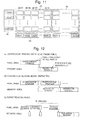
- Fig. 11 is a block diagram showing a schematic configuration for reading signals held in the memory sections within the memory area 3a through the previously described output line 23.
- one memory section unit 20 is selected by a combination of the horizontal shift registers HSR1-HSR320 and vertical shift registers VSR1-VSR104.
- the memory sections 22 are sequentially selected to extract pixel signals one after another. It should be noted that understanding the reading operation requires considering only the operation inside one memory section unit block 50 since different memory section unit blocks 50 having separate output lines 23 can be concurrently operated.
- the solid-state image sensor of the present embodiment has two major drive modes, i.e. the continuous reading mode and burst reading mode.
- the continuous reading mode corresponds to the first drive mode in the present invention
- the burst reading mode corresponds to the second drive mode.
- the following description initially explains schematic operations of these two drive modes with reference to Fig. 12.
- Fig. 12 is a schematic time chart of the continuous reading mode and burst reading mode.
- a detailed method of driving the solid-state image sensor of the present invention is hereinafter described, where the process from the photoelectric conversion in each pixel 10 through the storage of the resultant signal in one memory section 22 is initially described with reference to Figs. 13 to 16 .
- the solid-state image sensor of the present invention offers two different options for the drive mode: one drive mode is for a short photocharge storage time and the other for a relatively long photocharge storage time.
- the former mode is suitable for a photocharge storage time shorter than a range from 10 to 100 ⁇ sec.
- This drive mode can be preferably used when the imaging is performed at a high rate of one million frames per second or higher, which normally means that a burst reading mode is performed.
- Fig. 13 is a drive timing chart of the operation mode for a short photocharge storage time
- Fig. 14 is a schematic potential diagram inside the pixel 10 during this drive mode.
- C PD , C FD and C CS denote the capacitances stored in the photodiode 31, floating diffusion 33 and storage capacitor 36, respectively
- C FD +C CS denotes the combined capacitance of the floating diffusion 33 and storage capacitor 36.
- the signal ⁇ X which is a common control signal supplied to every pixel 10, is set to a high level to maintain both the selection transistors 38 and 41 within the source follower amplifier 43 in the ON state.
- the signals ⁇ T, ⁇ C and ⁇ R which are also common control signals, are set to a high level to turn on the transfer transistor 32, storage transistor 34 and reset transistor 35 (time t0), whereby the floating diffusion 33 and storage capacitor 36 are reset (or initialized).
- the photodiode 31 is completely depleted.
- the potential at this point in time is shown in Fig. 14a ).
- ⁇ R is set to a low level to turn off the reset transistor 35, whereupon a noise signal N2, which equivalently contains a random noise generating in the floating diffusion 33 and storage capacitor 36 and a fixed pattern noise resulting from a variation in the threshold voltage of the transistor 37 in the source follower amplifier 43, is generated in the floating diffusion 33 (refer to Fig. 14(b) ), and an output corresponding to this noise signal N2 appears in the pixel output line 141.
- a sampling pulse ⁇ N2 is given to the memory section 22 to turn on the sampling transistor 26d so that the noise signal N2 outputted through the pixel output line 141 is brought into and held by the capacitor 25d.
- ⁇ C is set to the low level to turn off the storage transistor 34, whereupon the signals stored in the floating diffusion 33 and storage capacitor 36 at this point in time are distributed to the floating diffusion 33 and the storage capacitor 36 according to the ratio of their capacitances C FD and C CS (refer to Fig. 14(c) ).
- a noise signal N1 which contains a random noise generated when ⁇ C was turned off and a fixed pattern noise resulting from a variation in the threshold voltage of the transistor 37 in the source follower amplifier 43, is generated in the floating diffusion 33, and an output corresponding to this noise signal N1 appears in the pixel output line 141.
- a sampling pulse ⁇ N1 is given to the memory section 22 to turn on the sampling transistor 26c so that the noise signal N1 outputted through the pixel output line 141 is brought into and held by the capacitor 25c.
- a sampling pulse ⁇ S1 is given to the memory section 22, with the storage transistor 34 in the OFF state, to turn on the sampling transistor 26a, whereby a signal corresponding to the charge stored in the floating diffusion 33 at that point in time (time t4) is extracted through the pixel output line 141 and held in the capacitor 25a (refer to Fig. 14(e) ).
- the signal stored in the floating diffusion 33 at this point in time results from the superposition of a noise signal N1 and a signal S1 corresponding to the charge before an overflow. Accordingly, the signal held in the capacitor 25a equals S1+N1, which does not reflect the amount of charge stored in the storage capacitor 36.
- ⁇ C is set to the high level to turn on the storage transistor 34, whereupon the charge held in the floating diffusion 33 at that point in time is mixed with the charge held in the storage capacitor 36 (refer to Fig. 14(f) ).
- a sampling pulse ⁇ S2 is given to the memory section 22 to turn on the sampling transistor 26b (time t5), whereby a signal corresponding to the charges held in the floating diffusion 33 and the storage capacitor 36, i.e. a signal resulting from the superposition of the noise signal N2 and the signal S2 corresponding to the charge after the overflow, is extracted through the pixel output line 141 and held in the capacitor 25b.
- the signal to be held in the capacitor 25b is S2+N2, which reflects the amount of charge stored in the storage capacitor 36.
- the signals S1+N1, S2+N2, N1 and N2 are respectively held in the four capacitors 25a, 25b, 25c and 25d included in one memory section 22.
- the noise signals N1 and N2 containing the random noise and fixed pattern noise are obtained separately from the other signals containing these noise signals.
- These signals can be respectively read from the capacitors 25a, 25b, 25c and 25d and then subjected to a subtracting operation by an analogue computing circuit (not shown) to obtain high S/N image signals free from the influence of the noise signals N1 and N2.
- Fig. 15 is a drive timing chart in the case where the photocharge storage time is relatively long
- Fig. 16 is a schematic potential diagram inside the pixel in this operation.
- the most significant difference from the case of the short photocharge storage time exists in that the transfer transistor 32 is turned off during the photocharge storage period so that the photocharges produced in the photodiode 31 will be stored in a depletion layer. Another difference is that, taking into account the long photocharge storage time, the selection transistors 38 and 41 of the source follower amplifier 43 are turned off for a predetermined period of time in order to reduce the power consumption.
- ⁇ T, ⁇ C and ⁇ R are set to high levels to turn on both the storage transistor 34 and reset transistor 35 (time t10), whereby the floating diffusion 33 and storage capacitor 36 are reset (or initialized). At this point in time, the photodiode 31 is completely depleted. The state of potential at this point in time is shown in Fig. 16a ).
- ⁇ R is set to the low level to turn off the reset transistor 35, whereupon a noise signal N2, which equivalently contains a random noise generating in the floating diffusion 33 and the storage capacitor 36 and a fixed pattern noise resulting from a variation in the threshold voltage of the transistor 37 in the source follower amplifier 43, is generated in the floating diffusion 33 (refer to Fig. 16(b) ), and an output corresponding to this noise signal N2 appears in the pixel output line 141.
- a sampling pulse ⁇ N2 is given to the memory section 22 to turn on the sampling transistor 26d, whereby the noise signal N2 is extracted through the pixel output line 141 and held in the capacitor 25d.
- ⁇ C is set to the low level to turn off the storage transistor 34, whereupon the signals stored in the floating diffusion 33 and storage capacitor 36 at this point in time are distributed to the floating diffusion 33 and storage capacitor 36 according to the ratio of their capacitances C FD and C CS .
- ⁇ T is set to the low level to turn off the transfer transistor 32
- ⁇ X is also set to the low level to turn off the two selection transistors 38 and 41 of the source follower amplifier 43 (time t12).
- a potential barrier is formed between the photodiode 31 and the floating diffusion 33, creating a condition where photocharges can be stored in the photodiode 31 (refer to Fig. 16(c) ).
- the photocharges produced by incident light falling onto the photodiode 31 are stored in the photodiode 31.
- a charge saturation occurs in the photodiode 31
- excessive charges overflow through the transfer transistor 32, to be stored in the floating diffusion 33 and superimposed on the noise signal that has been distributed as described previously. If the floating diffusion 33 is saturated by stronger incident light, the overflowing charges will be stored through the storage transistor 34 into the storage capacitor 36 (refer to Fig. 16(d) ).
- ⁇ X is set to the high level to turn on the selection transistors 38 and 41, after which a sampling pulse ⁇ N1 is given to the memory section 22 to turn on the sampling transistor 26c, whereby a noise signal N1 corresponding to the signal charge stored in the floating diffusion 33 at this point in time (time t13) is extracted through the pixel output line 14 and held in the capacitor 25c.
- the noise signal N1 at this point in time contains a fixed pattern noise due to a variation in the threshold voltage of the transistor 37 in the source follower amplifier 43. It should be noted that this signal contains not only the noise but also a portion of the photocharges produced by photoelectric conversion, which are also regarded as a noise in the present case.
- ⁇ T is set to the high level to turn on the transfer transistor 32, whereupon the photocharges stored in the photodiode 31 are completely transferred to the floating diffusion 33 (refer to Fig. 16(e) ).
- a sampling pulse ⁇ S1 is given to the memory section 22 to turn on the sampling transistor 26a, whereby a signal corresponding to the charge stored in the floating diffusion 33 is extracted through the pixel output line 14 and held in the capacitor 25a.
- This signal results from the superposition of the aforementioned noise signal N and the signal corresponding to the charge stored in the photodiode 31, i.e. the signal S1 before the overflow, and hence equals S1+N1.
- ⁇ C is set to the high level to turn on the storage transistor 34, whereupon the charge held in the floating diffusion 33 at that point in time is mixed with the charge held in the storage capacitor 36 (refer to Fig. 16(f) ).
- a sampling pulse ⁇ S2 is given to the memory section 22 to turn on the sampling transistor 26b (time t15), whereby a signal corresponding to the charges held in the floating diffusion 33 and Storage capacitor 36 are extracted through the pixel output line 141 and held in the capacitor 25b. This signal equals S2+N2.
- the signals S1+N1, S2+N2, N1 and N2 are respectively held in the four capacitors 25a, 25b, 25c and 25d included in one memory section 22.
- the noise signals N1 and N2 containing the random noise and fixed pattern noise are obtained separately from the other signals containing these noise signals.
- These signals can be respectively read from the capacitors 25a, 25b, 25c and 25d and then subjected to subtraction or other analogue computing to obtain high S/N image signals free from the influence of the noise signals N1 and N2. Since the charges that have overflowed from the floating diffusion 33 are not discarded but utilized, even a strong incident light barely causes saturation, so that the resultant signal can reflect the light. Thus, a wide dynamic range is ensured.
- This process is continued, for example, until a command signal for halting the imaging is externally given.
- the command signal for halting the imaging is given and the imaging is thereby discontinued, the latest 104 frames of image signals are held in the memory areas 3a and 3b. By sequentially reading these signals, a series of image signals corresponding to 104 frames can be obtained.
- the signals held in the capacitors 25 of each memory section 22 are read by sequentially turning on the reading transistors 27 connected to the same output line 23. Since the four reading transistors 27a-27d of the same memory section 22 are respectively connected to the different output lines 23a-23d, the signals held in each of the four capacitors 25a-25d in the same memory sections 22 can be simultaneously read. Using these signals, the subtracting operations of (S1+N1)-N1 and (S2+N2)-N2 can be performed by a subtraction circuit (now shown) provided inside or outside the sensor to extract the signals S1 and S2 free from the random noise and fixed pattern noise.
- Which of S1 and S2 should be used is determined with reference to an appropriate signal level equal to or lower than the saturation level of the signal S1; S1 is selected when the signal is equal to or higher than the reference level, and S2 when the signal is lower than me reference level. By performing this selection below the signal saturation level, it is possible to avoid the influence of saturation variation of S1.
- the reading order at the leftmost memory section unit block 50 in the 320 memory section units 20 corresponding to the first frame in Fig. 11 is hereinafter described.
- image signals of eleven pixels are sequentially read from the memory sections 22 in the left-to-right direction of the first horizontal row shown in Fig. 8 .
- This memory section unit 20-01 is selected by activating the horizontal shift register HSR1 and vertical shift register VSH1.
- the horizontal reading clock H-CLK produces a moving pulse signal that turns on the reading transistor 27 of the memory sections 22, one by one, from left to right in the horizontal direction.
- a clock V-CLK for shifting the vertical reading position is supplied, whereby the memory sections 22 in the next (second) row are selected.
- these memory sections 22 are similarly selected, from left to right, for the reading of eleven pixels.
- Such a process of reading pixel signals is repeated until the end of the twelfth row.
- the reading of pixel signals of the second frame is subsequently initiated. That is, as shown in Fig. 18 , the horizontal shift register HSR1 and the vertical shift register VSR2 are activated to select the leftmost memory section unit of the second row shown in Fig. 11 , and the reading operation is performed in the same order as in the case of the first frame. This process is repeated to perform the reading operation through the end of the 104 th frame.
- the continuous reading mode and burst reading mode of the present solid-state image sensor can be easily and quickly switched in response to an external control command since the differences between the two modes are rather miner ones that relate to the control signals supplied to the pixels, the drive signals tor controlling the horizontal shift registers and vertical shift registers and so on.
- a mode of the imaging operation of the present solid-state image sensor using the aforementioned switching operation is described.
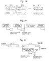
- Figs. 20 and 21 are schematic timing charts each showing one mode of the imaging operation using the present solid-state image sensor.
- the image signals that are read one frame after another by the previously described continuous reading mode are processed by a image processing circuit external to the solid-state image sensor (or, if possible, by a built-in circuit of the solid-state image sensor) to detect a movement of or change in an object of imagine.
- a image processing circuit external to the solid-state image sensor (or, if possible, by a built-in circuit of the solid-state image sensor) to detect a movement of or change in an object of imagine.
- various kinds of conventionally known motion detection processing techniques are available, such as using the differences in the image signals between a plurality of frames.
- the profess may detect a change or movement within a specific range of the image selected by a user rather than the entire image. When a movement of or change in an object has been recognized as a result of such a process, a corresponding trigger signal is produced.
- the operation mode changes from the continuous reading mode to the burst reading mode to perform high-speed imaging of 104 frames (or an appropriately specified number of frames).
- the pixel signals that have been read from the sensor in the burst reading mode are stored in an external frame memory. After the burst reading process for 104 frames (or an appropriately specified number of frames) is completed, the operation returns to the continuous reading mode.
- the example shown in Fig. 21 is basically a repetition of the storage or photocharges and the transfer of signals from each pixel at the repetition rate in the burst reading mode, and every time this process is repeated a predetermined number of frames, the storage of photocharges in the continuous reading mode and the sequential reading of the thereby obtained pixel signals to the outside are performed. In this sequential reading process, the storage of photocharges at the repetition rate in the burst reading mode and the transfer of signals from each pixel can be concurrently performed. Similar to the previous example, a movement of or change in an object is detected by an external image processing circuit and, based on the detection result, a trigger signal is generated.
- the signal transfer from each pixel to the memory section in the burst reading mode is halted, after which the writing of signals may also be halted with a delay corresponding to a predetermined period of time or predetermined number of frames from the generation of the trigger signal.
- the transistors that should be simultaneously turned on for reading may be selected in such a manner that the pixel sets neighboring each other in the horizontal and vertical directions in the pixel area 2 (2a or 2b) have an alternating boundary pattern as shown in Fig. 23(b) rather than an identical boundary pattern in both horizontal and vertical directions as in the previous example.
- This method is effective in reducing, to some extent, the decrease in the visual resolution due to the integration of pixel signals of a plurality of pixels.
- the aforementioned thin-out reading and summation of a plurality of pixels can also be performed by changing the control mode of the vertical shift register circuit and horizontal shift register circuit for driving the memory sections 22 within the memory area 3a and 3b; there is no influence on the configuration of the pixels 10 within the pixel area 2 (2a or 2b) or other designs of the sensor. Therefore, there is a high degree of freedom of changing the pixel signal reading method in the previously described manner.
Landscapes
- Engineering & Computer Science (AREA)
- Multimedia (AREA)
- Signal Processing (AREA)
- Transforming Light Signals Into Electric Signals (AREA)
- Solid State Image Pick-Up Elements (AREA)
Priority Applications (2)
| Application Number | Priority Date | Filing Date | Title |
|---|---|---|---|
| EP13179556.9A EP2663071B1 (fr) | 2007-09-05 | 2008-09-04 | Capteur d'image à l'état solide et son procédé de commande |
| EP13180147.4A EP2665256B1 (fr) | 2007-09-05 | 2008-09-04 | Capteur d'image à semi-conducteur et son procédé de commande |
Applications Claiming Priority (2)
| Application Number | Priority Date | Filing Date | Title |
|---|---|---|---|
| JP2007230179 | 2007-09-05 | ||
| PCT/JP2008/002426 WO2009031302A1 (fr) | 2007-09-05 | 2008-09-04 | Élément d'imagerie à semi-conducteurs et son procédé d'excitation |
Related Child Applications (5)
| Application Number | Title | Priority Date | Filing Date |
|---|---|---|---|
| EP13179556.9A Division-Into EP2663071B1 (fr) | 2007-09-05 | 2008-09-04 | Capteur d'image à l'état solide et son procédé de commande |
| EP13179556.9A Division EP2663071B1 (fr) | 2007-09-05 | 2008-09-04 | Capteur d'image à l'état solide et son procédé de commande |
| EP13180147.4A Division-Into EP2665256B1 (fr) | 2007-09-05 | 2008-09-04 | Capteur d'image à semi-conducteur et son procédé de commande |
| EP13180147.4A Division EP2665256B1 (fr) | 2007-09-05 | 2008-09-04 | Capteur d'image à semi-conducteur et son procédé de commande |
| EP13179566 Division-Into | 2013-08-07 |
Publications (3)
| Publication Number | Publication Date |
|---|---|
| EP2192765A1 true EP2192765A1 (fr) | 2010-06-02 |
| EP2192765A4 EP2192765A4 (fr) | 2010-08-11 |
| EP2192765B1 EP2192765B1 (fr) | 2015-11-11 |
Family
ID=40428626
Family Applications (3)
| Application Number | Title | Priority Date | Filing Date |
|---|---|---|---|
| EP13179556.9A Active EP2663071B1 (fr) | 2007-09-05 | 2008-09-04 | Capteur d'image à l'état solide et son procédé de commande |
| EP13180147.4A Active EP2665256B1 (fr) | 2007-09-05 | 2008-09-04 | Capteur d'image à semi-conducteur et son procédé de commande |
| EP08829005.1A Active EP2192765B1 (fr) | 2007-09-05 | 2008-09-04 | Capteur d'image à semi-conducteur et procédé de commande associé |
Family Applications Before (2)
| Application Number | Title | Priority Date | Filing Date |
|---|---|---|---|
| EP13179556.9A Active EP2663071B1 (fr) | 2007-09-05 | 2008-09-04 | Capteur d'image à l'état solide et son procédé de commande |
| EP13180147.4A Active EP2665256B1 (fr) | 2007-09-05 | 2008-09-04 | Capteur d'image à semi-conducteur et son procédé de commande |
Country Status (7)
| Country | Link |
|---|---|
| US (1) | US8482640B2 (fr) |
| EP (3) | EP2663071B1 (fr) |
| JP (1) | JP4844853B2 (fr) |
| KR (1) | KR101036596B1 (fr) |
| CN (1) | CN101796821B (fr) |
| TW (1) | TWI405462B (fr) |
| WO (1) | WO2009031302A1 (fr) |
Cited By (2)
| Publication number | Priority date | Publication date | Assignee | Title |
|---|---|---|---|---|
| US9030582B2 (en) | 2011-02-08 | 2015-05-12 | Shimadzu Corporation | Solid state image sensor and method for driving the same |
| EP3220628A4 (fr) * | 2014-11-20 | 2017-10-18 | Shimadzu Corporation | Détecteur optique |
Families Citing this family (30)
| Publication number | Priority date | Publication date | Assignee | Title |
|---|---|---|---|---|
| EP2192615A4 (fr) * | 2007-09-05 | 2011-07-27 | Univ Tohoku | Dispositif d'imagerie à semi-conducteurs et procédé de production de ce dernier |
| JP4978818B2 (ja) * | 2008-06-10 | 2012-07-18 | 国立大学法人東北大学 | 固体撮像素子及びその駆動方法 |
| JP5412152B2 (ja) * | 2009-03-18 | 2014-02-12 | 株式会社日立国際電気 | 撮像方法及び撮像装置 |
| JP2011204878A (ja) * | 2010-03-25 | 2011-10-13 | Sony Corp | 固体撮像デバイスおよび電子機器 |
| JP4657379B1 (ja) * | 2010-09-01 | 2011-03-23 | 株式会社ナックイメージテクノロジー | 高速度ビデオカメラ |
| US8937666B1 (en) * | 2012-10-09 | 2015-01-20 | Google Inc. | User interface for providing feedback for handheld image capture |
| JP6021613B2 (ja) * | 2012-11-29 | 2016-11-09 | キヤノン株式会社 | 撮像素子、撮像装置、および、撮像システム |
| JP2015060053A (ja) | 2013-09-18 | 2015-03-30 | 株式会社東芝 | 固体撮像装置、制御装置及び制御プログラム |
| JP6218799B2 (ja) | 2015-01-05 | 2017-10-25 | キヤノン株式会社 | 撮像素子及び撮像装置 |
| US10070088B2 (en) * | 2015-01-05 | 2018-09-04 | Canon Kabushiki Kaisha | Image sensor and image capturing apparatus for simultaneously performing focus detection and image generation |
| US9749548B2 (en) | 2015-01-22 | 2017-08-29 | Google Inc. | Virtual linebuffers for image signal processors |
| US9965824B2 (en) | 2015-04-23 | 2018-05-08 | Google Llc | Architecture for high performance, power efficient, programmable image processing |
| US9756268B2 (en) | 2015-04-23 | 2017-09-05 | Google Inc. | Line buffer unit for image processor |
| US9769356B2 (en) | 2015-04-23 | 2017-09-19 | Google Inc. | Two dimensional shift array for image processor |
| US10095479B2 (en) * | 2015-04-23 | 2018-10-09 | Google Llc | Virtual image processor instruction set architecture (ISA) and memory model and exemplary target hardware having a two-dimensional shift array structure |
| US9785423B2 (en) | 2015-04-23 | 2017-10-10 | Google Inc. | Compiler for translating between a virtual image processor instruction set architecture (ISA) and target hardware having a two-dimensional shift array structure |
| US10291813B2 (en) | 2015-04-23 | 2019-05-14 | Google Llc | Sheet generator for image processor |
| US9772852B2 (en) | 2015-04-23 | 2017-09-26 | Google Inc. | Energy efficient processor core architecture for image processor |
| JP6239026B2 (ja) * | 2015-05-29 | 2017-11-29 | キヤノン株式会社 | 撮像素子および撮像装置 |
| US10313641B2 (en) | 2015-12-04 | 2019-06-04 | Google Llc | Shift register with reduced wiring complexity |
| US9830150B2 (en) | 2015-12-04 | 2017-11-28 | Google Llc | Multi-functional execution lane for image processor |
| US10387988B2 (en) | 2016-02-26 | 2019-08-20 | Google Llc | Compiler techniques for mapping program code to a high performance, power efficient, programmable image processing hardware platform |
| US10204396B2 (en) | 2016-02-26 | 2019-02-12 | Google Llc | Compiler managed memory for image processor |
| US10380969B2 (en) | 2016-02-28 | 2019-08-13 | Google Llc | Macro I/O unit for image processor |
| US20180005346A1 (en) | 2016-07-01 | 2018-01-04 | Google Inc. | Core Processes For Block Operations On An Image Processor Having A Two-Dimensional Execution Lane Array and A Two-Dimensional Shift Register |
| US20180007302A1 (en) | 2016-07-01 | 2018-01-04 | Google Inc. | Block Operations For An Image Processor Having A Two-Dimensional Execution Lane Array and A Two-Dimensional Shift Register |
| US10546211B2 (en) | 2016-07-01 | 2020-01-28 | Google Llc | Convolutional neural network on programmable two dimensional image processor |
| US20180005059A1 (en) | 2016-07-01 | 2018-01-04 | Google Inc. | Statistics Operations On Two Dimensional Image Processor |
| JP7330124B2 (ja) * | 2020-03-19 | 2023-08-21 | 株式会社東芝 | 固体撮像装置 |
| US11698447B2 (en) * | 2020-07-17 | 2023-07-11 | Infineon Technologies Ag | Beam steering aware pixel clustering of segmented sensor area and implementing averaging algorithms for pixel processing |
Family Cites Families (21)
| Publication number | Priority date | Publication date | Assignee | Title |
|---|---|---|---|---|
| JPS62190753A (ja) | 1986-02-18 | 1987-08-20 | Agency Of Ind Science & Technol | 輪郭抽出用半導体装置 |
| JPS63174356A (ja) * | 1987-01-14 | 1988-07-18 | Agency Of Ind Science & Technol | 画像処理用半導体装置 |
| JPH0773339B2 (ja) | 1992-06-04 | 1995-08-02 | 学校法人近畿大学 | 撮影装置 |
| US6377304B1 (en) * | 1998-02-05 | 2002-04-23 | Nikon Corporation | Solid-state image-pickup devices exhibiting faster video-frame processing rates, and associated methods |
| JP4326050B2 (ja) | 1998-09-22 | 2009-09-02 | ハイスペック合資会社 | 高速撮像素子 |
| EP1166359A1 (fr) | 1999-03-04 | 2002-01-02 | Böhm, Markus | Dispositif capteur d'images |
| TW411705B (en) | 1999-03-15 | 2000-11-11 | Avision Inc | Charge transfer method for CCD image sensing device |
| WO2001026051A1 (fr) * | 1999-10-04 | 2001-04-12 | Hamamatsu Photonic K.K. | Systeme de camera assurant le traitement des images a grande vitesse |
| JP3704052B2 (ja) | 2000-03-28 | 2005-10-05 | リンク・リサーチ株式会社 | 高速撮像素子及び高速撮影装置 |
| JP2002354340A (ja) * | 2001-05-24 | 2002-12-06 | Olympus Optical Co Ltd | 撮像装置 |
| US7027092B2 (en) | 2001-09-17 | 2006-04-11 | Hewlett-Packard Development Company, L.P. | Image capture and storage device |
| US20030206236A1 (en) * | 2002-05-06 | 2003-11-06 | Agfa Corporation | CMOS digital image sensor system and method |
| US7586074B2 (en) * | 2003-02-17 | 2009-09-08 | Raytheon Company | Multi-mode high capacity dual integration direct injection detector input circuit |
| US7154075B2 (en) * | 2003-11-13 | 2006-12-26 | Micron Technology, Inc. | Method and apparatus for pixel signal binning and interpolation in column circuits of a sensor circuit |
| WO2005083790A1 (fr) * | 2004-02-27 | 2005-09-09 | Texas Instruments Japan Limited | Dispositif d’imagerie à semi-conducteur, capteur de ligne, capteur optique, et procede d’utilisation de dispositif d’imagerie à semi-conducteur |
| JP2005286677A (ja) * | 2004-03-30 | 2005-10-13 | Olympus Corp | 撮像装置 |
| GB0411648D0 (en) * | 2004-05-25 | 2004-06-30 | Fillfactory N V | Method and pixel for performing correlated double sampling |
| JP2006101479A (ja) * | 2004-09-02 | 2006-04-13 | Canon Inc | 固体撮像装置及びそれを用いたカメラ |
| JP5066704B2 (ja) | 2005-02-04 | 2012-11-07 | 国立大学法人東北大学 | 固体撮像装置、および固体撮像装置の動作方法 |
| WO2007010753A1 (fr) * | 2005-07-15 | 2007-01-25 | Matsushita Electric Industrial Co., Ltd. | Dispositif et procédé de traitement de données de traitement d'image, et élément de traitement d'image |
| JP2007166581A (ja) * | 2005-11-16 | 2007-06-28 | Matsushita Electric Ind Co Ltd | 高速撮影用固体撮像装置 |
-
2008
- 2008-09-04 WO PCT/JP2008/002426 patent/WO2009031302A1/fr not_active Ceased
- 2008-09-04 CN CN200880105556XA patent/CN101796821B/zh active Active
- 2008-09-04 JP JP2009531124A patent/JP4844853B2/ja active Active
- 2008-09-04 US US12/676,505 patent/US8482640B2/en active Active
- 2008-09-04 EP EP13179556.9A patent/EP2663071B1/fr active Active
- 2008-09-04 EP EP13180147.4A patent/EP2665256B1/fr active Active
- 2008-09-04 KR KR1020107003061A patent/KR101036596B1/ko active Active
- 2008-09-04 EP EP08829005.1A patent/EP2192765B1/fr active Active
- 2008-09-05 TW TW097134048A patent/TWI405462B/zh active
Cited By (2)
| Publication number | Priority date | Publication date | Assignee | Title |
|---|---|---|---|---|
| US9030582B2 (en) | 2011-02-08 | 2015-05-12 | Shimadzu Corporation | Solid state image sensor and method for driving the same |
| EP3220628A4 (fr) * | 2014-11-20 | 2017-10-18 | Shimadzu Corporation | Détecteur optique |
Also Published As
| Publication number | Publication date |
|---|---|
| KR101036596B1 (ko) | 2011-05-24 |
| TW200920118A (en) | 2009-05-01 |
| EP2192765A4 (fr) | 2010-08-11 |
| JP4844853B2 (ja) | 2011-12-28 |
| JPWO2009031302A1 (ja) | 2010-12-09 |
| US8482640B2 (en) | 2013-07-09 |
| TWI405462B (zh) | 2013-08-11 |
| US20100188538A1 (en) | 2010-07-29 |
| EP2663071A3 (fr) | 2013-11-20 |
| KR20100039884A (ko) | 2010-04-16 |
| CN101796821B (zh) | 2012-12-12 |
| EP2665256A1 (fr) | 2013-11-20 |
| EP2192765B1 (fr) | 2015-11-11 |
| WO2009031302A1 (fr) | 2009-03-12 |
| EP2663071A2 (fr) | 2013-11-13 |
| EP2665256B1 (fr) | 2015-11-18 |
| EP2663071B1 (fr) | 2015-11-18 |
| CN101796821A (zh) | 2010-08-04 |
Similar Documents
| Publication | Publication Date | Title |
|---|---|---|
| EP2192765B1 (fr) | Capteur d'image à semi-conducteur et procédé de commande associé | |
| US8269838B2 (en) | Solid-state image sensor and imaging device | |
| EP2299696B1 (fr) | Capteur d'image à semi-conducteur et procédé de commande associé | |
| EP2190185B1 (fr) | Élément d'imagerie à semi-conducteurs | |
| US8569805B2 (en) | Solid-state image sensor and method for producing the same | |
| US8541731B2 (en) | Solid-state image sensor | |
| KR20090086091A (ko) | 고체 촬상 장치, 고체 촬상 장치의 구동 방법 및 촬상 장치 |
Legal Events
| Date | Code | Title | Description |
|---|---|---|---|
| PUAI | Public reference made under article 153(3) epc to a published international application that has entered the european phase |
Free format text: ORIGINAL CODE: 0009012 |
|
| 17P | Request for examination filed |
Effective date: 20100322 |
|
| AK | Designated contracting states |
Kind code of ref document: A1 Designated state(s): AT BE BG CH CY CZ DE DK EE ES FI FR GB GR HR HU IE IS IT LI LT LU LV MC MT NL NO PL PT RO SE SI SK TR |
|
| AX | Request for extension of the european patent |
Extension state: AL BA MK RS |
|
| A4 | Supplementary search report drawn up and despatched |
Effective date: 20100713 |
|
| RIC1 | Information provided on ipc code assigned before grant |
Ipc: H01L 27/146 20060101ALI20100707BHEP Ipc: H04N 5/335 20060101AFI20090327BHEP |
|
| DAX | Request for extension of the european patent (deleted) | ||
| 17Q | First examination report despatched |
Effective date: 20110803 |
|
| GRAP | Despatch of communication of intention to grant a patent |
Free format text: ORIGINAL CODE: EPIDOSNIGR1 |
|
| INTG | Intention to grant announced |
Effective date: 20150120 |
|
| GRAP | Despatch of communication of intention to grant a patent |
Free format text: ORIGINAL CODE: EPIDOSNIGR1 |
|
| INTG | Intention to grant announced |
Effective date: 20150331 |
|
| GRAS | Grant fee paid |
Free format text: ORIGINAL CODE: EPIDOSNIGR3 |
|
| GRAA | (expected) grant |
Free format text: ORIGINAL CODE: 0009210 |
|
| AK | Designated contracting states |
Kind code of ref document: B1 Designated state(s): AT BE BG CH CY CZ DE DK EE ES FI FR GB GR HR HU IE IS IT LI LT LU LV MC MT NL NO PL PT RO SE SI SK TR |
|
| REG | Reference to a national code |
Ref country code: GB Ref legal event code: FG4D |
|
| REG | Reference to a national code |
Ref country code: CH Ref legal event code: EP |
|
| REG | Reference to a national code |
Ref country code: IE Ref legal event code: FG4D |
|
| REG | Reference to a national code |
Ref country code: AT Ref legal event code: REF Ref document number: 760956 Country of ref document: AT Kind code of ref document: T Effective date: 20151215 |
|
| REG | Reference to a national code |
Ref country code: DE Ref legal event code: R096 Ref document number: 602008041175 Country of ref document: DE |
|
| REG | Reference to a national code |
Ref country code: NL Ref legal event code: FP |
|
| REG | Reference to a national code |
Ref country code: LT Ref legal event code: MG4D |
|
| REG | Reference to a national code |
Ref country code: AT Ref legal event code: MK05 Ref document number: 760956 Country of ref document: AT Kind code of ref document: T Effective date: 20151111 |
|
| PG25 | Lapsed in a contracting state [announced via postgrant information from national office to epo] |
Ref country code: LT Free format text: LAPSE BECAUSE OF FAILURE TO SUBMIT A TRANSLATION OF THE DESCRIPTION OR TO PAY THE FEE WITHIN THE PRESCRIBED TIME-LIMIT Effective date: 20151111 Ref country code: IT Free format text: LAPSE BECAUSE OF FAILURE TO SUBMIT A TRANSLATION OF THE DESCRIPTION OR TO PAY THE FEE WITHIN THE PRESCRIBED TIME-LIMIT Effective date: 20151111 Ref country code: HR Free format text: LAPSE BECAUSE OF FAILURE TO SUBMIT A TRANSLATION OF THE DESCRIPTION OR TO PAY THE FEE WITHIN THE PRESCRIBED TIME-LIMIT Effective date: 20151111 Ref country code: ES Free format text: LAPSE BECAUSE OF FAILURE TO SUBMIT A TRANSLATION OF THE DESCRIPTION OR TO PAY THE FEE WITHIN THE PRESCRIBED TIME-LIMIT Effective date: 20151111 Ref country code: IS Free format text: LAPSE BECAUSE OF FAILURE TO SUBMIT A TRANSLATION OF THE DESCRIPTION OR TO PAY THE FEE WITHIN THE PRESCRIBED TIME-LIMIT Effective date: 20160311 Ref country code: NO Free format text: LAPSE BECAUSE OF FAILURE TO SUBMIT A TRANSLATION OF THE DESCRIPTION OR TO PAY THE FEE WITHIN THE PRESCRIBED TIME-LIMIT Effective date: 20160211 |
|
| PG25 | Lapsed in a contracting state [announced via postgrant information from national office to epo] |
Ref country code: PT Free format text: LAPSE BECAUSE OF FAILURE TO SUBMIT A TRANSLATION OF THE DESCRIPTION OR TO PAY THE FEE WITHIN THE PRESCRIBED TIME-LIMIT Effective date: 20160311 Ref country code: GR Free format text: LAPSE BECAUSE OF FAILURE TO SUBMIT A TRANSLATION OF THE DESCRIPTION OR TO PAY THE FEE WITHIN THE PRESCRIBED TIME-LIMIT Effective date: 20160212 Ref country code: PL Free format text: LAPSE BECAUSE OF FAILURE TO SUBMIT A TRANSLATION OF THE DESCRIPTION OR TO PAY THE FEE WITHIN THE PRESCRIBED TIME-LIMIT Effective date: 20151111 Ref country code: LV Free format text: LAPSE BECAUSE OF FAILURE TO SUBMIT A TRANSLATION OF THE DESCRIPTION OR TO PAY THE FEE WITHIN THE PRESCRIBED TIME-LIMIT Effective date: 20151111 Ref country code: AT Free format text: LAPSE BECAUSE OF FAILURE TO SUBMIT A TRANSLATION OF THE DESCRIPTION OR TO PAY THE FEE WITHIN THE PRESCRIBED TIME-LIMIT Effective date: 20151111 Ref country code: FI Free format text: LAPSE BECAUSE OF FAILURE TO SUBMIT A TRANSLATION OF THE DESCRIPTION OR TO PAY THE FEE WITHIN THE PRESCRIBED TIME-LIMIT Effective date: 20151111 Ref country code: SE Free format text: LAPSE BECAUSE OF FAILURE TO SUBMIT A TRANSLATION OF THE DESCRIPTION OR TO PAY THE FEE WITHIN THE PRESCRIBED TIME-LIMIT Effective date: 20151111 |
|
| PG25 | Lapsed in a contracting state [announced via postgrant information from national office to epo] |
Ref country code: CZ Free format text: LAPSE BECAUSE OF FAILURE TO SUBMIT A TRANSLATION OF THE DESCRIPTION OR TO PAY THE FEE WITHIN THE PRESCRIBED TIME-LIMIT Effective date: 20151111 |
|
| REG | Reference to a national code |
Ref country code: DE Ref legal event code: R097 Ref document number: 602008041175 Country of ref document: DE |
|
| REG | Reference to a national code |
Ref country code: FR Ref legal event code: PLFP Year of fee payment: 9 |
|
| PG25 | Lapsed in a contracting state [announced via postgrant information from national office to epo] |
Ref country code: EE Free format text: LAPSE BECAUSE OF FAILURE TO SUBMIT A TRANSLATION OF THE DESCRIPTION OR TO PAY THE FEE WITHIN THE PRESCRIBED TIME-LIMIT Effective date: 20151111 Ref country code: DK Free format text: LAPSE BECAUSE OF FAILURE TO SUBMIT A TRANSLATION OF THE DESCRIPTION OR TO PAY THE FEE WITHIN THE PRESCRIBED TIME-LIMIT Effective date: 20151111 Ref country code: SK Free format text: LAPSE BECAUSE OF FAILURE TO SUBMIT A TRANSLATION OF THE DESCRIPTION OR TO PAY THE FEE WITHIN THE PRESCRIBED TIME-LIMIT Effective date: 20151111 Ref country code: RO Free format text: LAPSE BECAUSE OF FAILURE TO SUBMIT A TRANSLATION OF THE DESCRIPTION OR TO PAY THE FEE WITHIN THE PRESCRIBED TIME-LIMIT Effective date: 20151111 |
|
| PLBE | No opposition filed within time limit |
Free format text: ORIGINAL CODE: 0009261 |
|
| STAA | Information on the status of an ep patent application or granted ep patent |
Free format text: STATUS: NO OPPOSITION FILED WITHIN TIME LIMIT |
|
| 26N | No opposition filed |
Effective date: 20160812 |
|
| PG25 | Lapsed in a contracting state [announced via postgrant information from national office to epo] |
Ref country code: SI Free format text: LAPSE BECAUSE OF FAILURE TO SUBMIT A TRANSLATION OF THE DESCRIPTION OR TO PAY THE FEE WITHIN THE PRESCRIBED TIME-LIMIT Effective date: 20151111 |
|
| PG25 | Lapsed in a contracting state [announced via postgrant information from national office to epo] |
Ref country code: BE Free format text: LAPSE BECAUSE OF FAILURE TO SUBMIT A TRANSLATION OF THE DESCRIPTION OR TO PAY THE FEE WITHIN THE PRESCRIBED TIME-LIMIT Effective date: 20151111 |
|
| PG25 | Lapsed in a contracting state [announced via postgrant information from national office to epo] |
Ref country code: MC Free format text: LAPSE BECAUSE OF FAILURE TO SUBMIT A TRANSLATION OF THE DESCRIPTION OR TO PAY THE FEE WITHIN THE PRESCRIBED TIME-LIMIT Effective date: 20151111 |
|
| REG | Reference to a national code |
Ref country code: CH Ref legal event code: PL |
|
| REG | Reference to a national code |
Ref country code: IE Ref legal event code: MM4A |
|
| PG25 | Lapsed in a contracting state [announced via postgrant information from national office to epo] |
Ref country code: CH Free format text: LAPSE BECAUSE OF NON-PAYMENT OF DUE FEES Effective date: 20160930 Ref country code: IE Free format text: LAPSE BECAUSE OF NON-PAYMENT OF DUE FEES Effective date: 20160904 Ref country code: LI Free format text: LAPSE BECAUSE OF NON-PAYMENT OF DUE FEES Effective date: 20160930 |
|
| REG | Reference to a national code |
Ref country code: FR Ref legal event code: PLFP Year of fee payment: 10 |
|
| PG25 | Lapsed in a contracting state [announced via postgrant information from national office to epo] |
Ref country code: LU Free format text: LAPSE BECAUSE OF NON-PAYMENT OF DUE FEES Effective date: 20160904 |
|
| PG25 | Lapsed in a contracting state [announced via postgrant information from national office to epo] |
Ref country code: CY Free format text: LAPSE BECAUSE OF FAILURE TO SUBMIT A TRANSLATION OF THE DESCRIPTION OR TO PAY THE FEE WITHIN THE PRESCRIBED TIME-LIMIT Effective date: 20151111 Ref country code: HU Free format text: LAPSE BECAUSE OF FAILURE TO SUBMIT A TRANSLATION OF THE DESCRIPTION OR TO PAY THE FEE WITHIN THE PRESCRIBED TIME-LIMIT; INVALID AB INITIO Effective date: 20080904 |
|
| PG25 | Lapsed in a contracting state [announced via postgrant information from national office to epo] |
Ref country code: MT Free format text: LAPSE BECAUSE OF NON-PAYMENT OF DUE FEES Effective date: 20160930 Ref country code: TR Free format text: LAPSE BECAUSE OF FAILURE TO SUBMIT A TRANSLATION OF THE DESCRIPTION OR TO PAY THE FEE WITHIN THE PRESCRIBED TIME-LIMIT Effective date: 20151111 |
|
| PG25 | Lapsed in a contracting state [announced via postgrant information from national office to epo] |
Ref country code: BG Free format text: LAPSE BECAUSE OF FAILURE TO SUBMIT A TRANSLATION OF THE DESCRIPTION OR TO PAY THE FEE WITHIN THE PRESCRIBED TIME-LIMIT Effective date: 20151111 |
|
| REG | Reference to a national code |
Ref country code: FR Ref legal event code: PLFP Year of fee payment: 11 |
|
| REG | Reference to a national code |
Ref country code: DE Ref legal event code: R079 Ref document number: 602008041175 Country of ref document: DE Free format text: PREVIOUS MAIN CLASS: H04N0005335000 Ipc: H04N0025000000 |
|
| PGFP | Annual fee paid to national office [announced via postgrant information from national office to epo] |
Ref country code: NL Payment date: 20250814 Year of fee payment: 18 |
|
| PGFP | Annual fee paid to national office [announced via postgrant information from national office to epo] |
Ref country code: DE Payment date: 20250730 Year of fee payment: 18 |
|
| PGFP | Annual fee paid to national office [announced via postgrant information from national office to epo] |
Ref country code: GB Payment date: 20250731 Year of fee payment: 18 |
|
| PGFP | Annual fee paid to national office [announced via postgrant information from national office to epo] |
Ref country code: FR Payment date: 20250808 Year of fee payment: 18 |