EP2193468B1 - 3d-abbildung einzelner halbleiternanokristalle mit hoher auflösung - Google Patents
3d-abbildung einzelner halbleiternanokristalle mit hoher auflösung Download PDFInfo
- Publication number
- EP2193468B1 EP2193468B1 EP08865911.5A EP08865911A EP2193468B1 EP 2193468 B1 EP2193468 B1 EP 2193468B1 EP 08865911 A EP08865911 A EP 08865911A EP 2193468 B1 EP2193468 B1 EP 2193468B1
- Authority
- EP
- European Patent Office
- Prior art keywords
- nanocrystal
- radius
- nanocrystals
- determining
- semiconductor
- Prior art date
- Legal status (The legal status is an assumption and is not a legal conclusion. Google has not performed a legal analysis and makes no representation as to the accuracy of the status listed.)
- Active
Links
Images


Classifications
-
- G—PHYSICS
- G01—MEASURING; TESTING
- G01N—INVESTIGATING OR ANALYSING MATERIALS BY DETERMINING THEIR CHEMICAL OR PHYSICAL PROPERTIES
- G01N21/00—Investigating or analysing materials by the use of optical means, i.e. using sub-millimetre waves, infrared, visible or ultraviolet light
- G01N21/62—Systems in which the material investigated is excited whereby it emits light or causes a change in wavelength of the incident light
- G01N21/63—Systems in which the material investigated is excited whereby it emits light or causes a change in wavelength of the incident light optically excited
- G01N21/64—Fluorescence; Phosphorescence
- G01N21/645—Specially adapted constructive features of fluorimeters
- G01N21/6456—Spatial resolved fluorescence measurements; Imaging
- G01N21/6458—Fluorescence microscopy
-
- G—PHYSICS
- G01—MEASURING; TESTING
- G01N—INVESTIGATING OR ANALYSING MATERIALS BY DETERMINING THEIR CHEMICAL OR PHYSICAL PROPERTIES
- G01N21/00—Investigating or analysing materials by the use of optical means, i.e. using sub-millimetre waves, infrared, visible or ultraviolet light
- G01N21/62—Systems in which the material investigated is excited whereby it emits light or causes a change in wavelength of the incident light
- G01N21/63—Systems in which the material investigated is excited whereby it emits light or causes a change in wavelength of the incident light optically excited
- G01N21/64—Fluorescence; Phosphorescence
- G01N21/6428—Measuring fluorescence of fluorescent products of reactions or of fluorochrome labelled reactive substances, e.g. measuring quenching effects, using measuring "optrodes"
-
- G—PHYSICS
- G01—MEASURING; TESTING
- G01N—INVESTIGATING OR ANALYSING MATERIALS BY DETERMINING THEIR CHEMICAL OR PHYSICAL PROPERTIES
- G01N33/00—Investigating or analysing materials by specific methods not covered by groups G01N1/00 - G01N31/00
- G01N33/48—Biological material, e.g. blood, urine; Haemocytometers
- G01N33/50—Chemical analysis of biological material, e.g. blood, urine; Testing involving biospecific ligand binding methods; Immunological testing
- G01N33/58—Chemical analysis of biological material, e.g. blood, urine; Testing involving biospecific ligand binding methods; Immunological testing involving labelled substances
- G01N33/588—Chemical analysis of biological material, e.g. blood, urine; Testing involving biospecific ligand binding methods; Immunological testing involving labelled substances with semiconductor nanocrystal label, e.g. quantum dots
-
- B—PERFORMING OPERATIONS; TRANSPORTING
- B82—NANOTECHNOLOGY
- B82Y—SPECIFIC USES OR APPLICATIONS OF NANOSTRUCTURES; MEASUREMENT OR ANALYSIS OF NANOSTRUCTURES; MANUFACTURE OR TREATMENT OF NANOSTRUCTURES
- B82Y15/00—Nanotechnology for interacting, sensing or actuating, e.g. quantum dots as markers in protein assays or molecular motors
-
- B—PERFORMING OPERATIONS; TRANSPORTING
- B82—NANOTECHNOLOGY
- B82Y—SPECIFIC USES OR APPLICATIONS OF NANOSTRUCTURES; MEASUREMENT OR ANALYSIS OF NANOSTRUCTURES; MANUFACTURE OR TREATMENT OF NANOSTRUCTURES
- B82Y30/00—Nanotechnology for materials or surface science, e.g. nanocomposites
-
- G—PHYSICS
- G01—MEASURING; TESTING
- G01N—INVESTIGATING OR ANALYSING MATERIALS BY DETERMINING THEIR CHEMICAL OR PHYSICAL PROPERTIES
- G01N21/00—Investigating or analysing materials by the use of optical means, i.e. using sub-millimetre waves, infrared, visible or ultraviolet light
- G01N21/62—Systems in which the material investigated is excited whereby it emits light or causes a change in wavelength of the incident light
- G01N21/63—Systems in which the material investigated is excited whereby it emits light or causes a change in wavelength of the incident light optically excited
- G01N21/64—Fluorescence; Phosphorescence
- G01N21/6428—Measuring fluorescence of fluorescent products of reactions or of fluorochrome labelled reactive substances, e.g. measuring quenching effects, using measuring "optrodes"
- G01N2021/6439—Measuring fluorescence of fluorescent products of reactions or of fluorochrome labelled reactive substances, e.g. measuring quenching effects, using measuring "optrodes" with indicators, stains, dyes, tags, labels, marks
- G01N2021/6441—Measuring fluorescence of fluorescent products of reactions or of fluorochrome labelled reactive substances, e.g. measuring quenching effects, using measuring "optrodes" with indicators, stains, dyes, tags, labels, marks with two or more labels
-
- Y—GENERAL TAGGING OF NEW TECHNOLOGICAL DEVELOPMENTS; GENERAL TAGGING OF CROSS-SECTIONAL TECHNOLOGIES SPANNING OVER SEVERAL SECTIONS OF THE IPC; TECHNICAL SUBJECTS COVERED BY FORMER USPC CROSS-REFERENCE ART COLLECTIONS [XRACs] AND DIGESTS
- Y10—TECHNICAL SUBJECTS COVERED BY FORMER USPC
- Y10T—TECHNICAL SUBJECTS COVERED BY FORMER US CLASSIFICATION
- Y10T428/00—Stock material or miscellaneous articles
- Y10T428/12—All metal or with adjacent metals
- Y10T428/12014—All metal or with adjacent metals having metal particles
- Y10T428/12028—Composite; i.e., plural, adjacent, spatially distinct metal components [e.g., layers, etc.]
-
- Y—GENERAL TAGGING OF NEW TECHNOLOGICAL DEVELOPMENTS; GENERAL TAGGING OF CROSS-SECTIONAL TECHNOLOGIES SPANNING OVER SEVERAL SECTIONS OF THE IPC; TECHNICAL SUBJECTS COVERED BY FORMER USPC CROSS-REFERENCE ART COLLECTIONS [XRACs] AND DIGESTS
- Y10—TECHNICAL SUBJECTS COVERED BY FORMER USPC
- Y10T—TECHNICAL SUBJECTS COVERED BY FORMER US CLASSIFICATION
- Y10T428/00—Stock material or miscellaneous articles
- Y10T428/29—Coated or structually defined flake, particle, cell, strand, strand portion, rod, filament, macroscopic fiber or mass thereof
- Y10T428/2913—Rod, strand, filament or fiber
- Y10T428/2933—Coated or with bond, impregnation or core
- Y10T428/294—Coated or with bond, impregnation or core including metal or compound thereof [excluding glass, ceramic and asbestos]
-
- Y—GENERAL TAGGING OF NEW TECHNOLOGICAL DEVELOPMENTS; GENERAL TAGGING OF CROSS-SECTIONAL TECHNOLOGIES SPANNING OVER SEVERAL SECTIONS OF THE IPC; TECHNICAL SUBJECTS COVERED BY FORMER USPC CROSS-REFERENCE ART COLLECTIONS [XRACs] AND DIGESTS
- Y10—TECHNICAL SUBJECTS COVERED BY FORMER USPC
- Y10T—TECHNICAL SUBJECTS COVERED BY FORMER US CLASSIFICATION
- Y10T428/00—Stock material or miscellaneous articles
- Y10T428/29—Coated or structually defined flake, particle, cell, strand, strand portion, rod, filament, macroscopic fiber or mass thereof
- Y10T428/2982—Particulate matter [e.g., sphere, flake, etc.]
- Y10T428/2991—Coated
-
- Y—GENERAL TAGGING OF NEW TECHNOLOGICAL DEVELOPMENTS; GENERAL TAGGING OF CROSS-SECTIONAL TECHNOLOGIES SPANNING OVER SEVERAL SECTIONS OF THE IPC; TECHNICAL SUBJECTS COVERED BY FORMER USPC CROSS-REFERENCE ART COLLECTIONS [XRACs] AND DIGESTS
- Y10—TECHNICAL SUBJECTS COVERED BY FORMER USPC
- Y10T—TECHNICAL SUBJECTS COVERED BY FORMER US CLASSIFICATION
- Y10T436/00—Chemistry: analytical and immunological testing
- Y10T436/14—Heterocyclic carbon compound [i.e., O, S, N, Se, Te, as only ring hetero atom]
- Y10T436/141111—Diverse hetero atoms in same or different rings [e.g., alkaloids, opiates, etc.]
Definitions
- the invention relates to high resolution 3D imaging of single semiconductor nanocrystals.
- Semiconductor nanocrystals are photostable fluorophores with narrow emission spectra tunable through visible and near-infrared wavelengths, large molar extinction coefficients, and high quantum yields. These properties make semiconductor nanocrystals powerful tools for labeling and optical sensing in biological, biomedical, and environmental contexts.
- the exceptional brightness and photostability of semiconductor nanocrystals give them great potential for analyzing biological events at the single molecule level.
- current nanocrystals designed for cellular labeling applications suffer a tradeoff between size, non-specific binding, and derivatizability.
- Nanocrystals generally include an inorganic nanoparticle that is surrounded by a layer of organic ligands. This organic ligand shell is critical to the nanocrystals for processing, binding to specific other moieties, and incorporation into various substrates. Nanocrystals can be stored in their growth solution, which contains a large excess of ligands such as alkyl phosphines and alkyl phosphine oxides, for long periods without noticeable degradation. For most applications, particularly aqueous applications, nanocrystals must be processed outside of their growth solution and transferred into various chemical environments. However, nanocrystals often lose their high fluorescence or become irreversibly aggregated when removed from their growth solution.
- the article, " Quantum Dots Spectrally distinguish multiple species within the tumor milieu in vivo"; Nature Medicine; 2005-05-08; STROH M; ET AL; VOL 11, NR 6, pages 678-682 concerns dynamic studies of tumor pathophysiology using multiphoton microscopy techniques in transgenic mice using quantum dot preparations which are fluorescent colloidal semiconductor nanocrystals.
- the studies include imaging tissues using quantum dot markings which are tunable by both size and chemical composition e.g. to image and differentiate tumor vessels from both the perivascular cells and the matrix.
- Single-particle tracking can give unprecedented understanding of the motion of cell surface proteins, free from the simplification of ensemble averaging.
- single-particle tracking is complicated by fluorophore photobleaching, probe multivalency, the size of the labeling probe, and dissociation of the probe from the target.
- Semiconductor nanocrystals have the intrinsic advantages for single particle tracking of brightness and photostability.
- a lens-based optical microscope can provide a resolution only close to half of the wavelength of light, on the order of hundred of nanometers for visible light.
- a nanocrystal-based tracking method which provides nanometer spatial resolution (e.g., on the order of 10 nm) in three dimensions.
- the tracking method can be used in tracking objects and structures (for example, biological objects and structures) on a micro- or nano-meter scale. The method to three dimensionally map a -350 nm thick polysaccharide layer called the glycocalyx on bovine aortic endothelial cells, and to study the mechanical properties of the polysaccharide layer under flow.
- the invention concerns a method imaging a microscopic object as defined in appended claim 1.
- Calculating the relative depths of the first and second semiconductor nanocrystals can include measuring a radius of the first semiconductor nanocrystal as it appears in each of the first and second fluorescence images. Measuring the radius includes measuring a radius of a local intensity maximum. When there are multiple local intensity maxima, the local intensity maximum having the greatest radius is chosen. Measuring the radius includes measuring a radius at a plurality of different angles. Measuring the radius includes determining a radial intensity profile. Determining the radial intensity profile includes calculating an integrated radial intensity profile for a plurality of different angles. The method can include fitting the radial intensity profile with one or more Gaussian curves.
- the method can include correlating the measured radius of the first semiconductor nanocrystal with the relative depth of the first semiconductor nanocrystal.
- the method can include determining relative three-dimensional coordinates of the first and second semiconductor nanocrystals based at least in part on the first and second fluorescence images.
- the method can include determining a three-dimensional shape of the object based at least in part on the relative three-dimensional coordinates of the first and second semiconductor nanocrystals.
- the object includes a biological structure.
- the biological structure can include a cell.
- the first semiconductor nanocrystal is associated with a moiety having a specific affinity for a biomolecule.
- the method can include tracking the location of at least one semiconductor nanocrystal as a function of time. Tracking the location can include determining three-dimensional coordinates for the semiconductor nanocrystal.
- the invention concerns a method imaging a microscopic object as defined in appended claim 11.
- the x -, y- and z -coordinates each individually can have a precision of ⁇ 15 nm or less, or a precision of ⁇ 10 nm or less. In some embodiments, at least one of the x - and y- coordinates can have a precision of ⁇ 5 nm or less, and the z-coordinate can have a precision of ⁇ 10 nm or less.
- Determining a z-coordinate from the radius of the nanocrystal image includes determining a radial intensity profile. Determining the radial intensity profile includes calculating an integrated radial intensity profile for a plurality of different angles. The method can include fitting the radial intensity profile with one or more Gaussian curves.
- Recording a fluorescence image of a semiconductor nanocrystal can include recording fluorescence images of a plurality of semiconductor nanocrystals in a single fluorescence image.
- Recording a fluorescence image of a semiconductor nanocrystal can include recording a first fluorescence image of a field at a first emission wavelength or range of wavelengths, and recording a second fluorescence image of the field at a second emission wavelength or range of wavelengths.
- the method can include moving the field in the z-direction, and repeating the steps of recording a first image of the field at a first emission wavelength or range of wavelengths, and recording a second image of the field at a second emission wavelength or range of wavelengths.
- An apparatus for imaging a microscopic object includes an objective lens configured to image a microscopic object arranged on a nanopositioner stage, a light source configured to simultaneously excite fluorescence from at least a first and a second semiconductor nanocrystal associated with the microscopic object, and a camera configured to record a first fluorescence image of the first and second semiconductor nanocrystals at a first focal depth and to record a second fluorescence image of the first and second semiconductor nanocrystals at a second focal depth different from the first focal depth.
- the apparatus can include a computer system configured to calculate the relative depths of the first and second semiconductor nanocrystals by measuring a radius of the first semiconductor nanocrystal as it appears in each of the first and second fluorescence images.
- the computer system can be further configured to measure the radius by calculating an integrated radial intensity profile for a plurality of different angles and fitting the radial intensity profile with one or more Gaussian curves.
- One goal of cellular imaging is to observe in living cells the movement of single biomolecules.
- Single molecules imaging in vitro has proved its ability to give the ultimate in sensitivity, detecting low abundance biomolecules such as miRNA or virus particles (see, e.g., Neely, L.A., et al., (2006). Nat. Methods 3, 41-46 ; and Agrawal, A., et al. (2006). Anal. Chem. 78, 1061-1070 .
- Semiconductor nanocrystals provide certain advantages in tracking the movement of single particles. Single semiconductor nanocrystals are bright enough to be seen easily on a wide field fluorescence microscope, without the need for TIRF, and are extremely photostable ( Gao, X., et al. (2005). Curr.Opin.Biotechnol. 16, 63 72 ).
- Ordinary light microscopy is limited to resolving objects a few hundred nanometers in size.
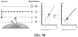
- Defocused imaging can locate the depth of particles with high resolution. See, e.g., M. Speidel, A. Jonas, and F. E., Opt. Lett. 28, 69 (2003 ) (" Speidel"). Briefly, the apparent radius of a point object, when in focus, can be described by: r ⁇ 0.61 ⁇ ⁇ / NA where NA is the numerical aperture of the objective lens. As the object undergoes displacement in the z -direction (i.e., orthogonal to the focal plane), the image of the object becomes defocused.
- interference rings become apparent as the z displacement increases,.
- the z displacement is linearly correlated with radius of the outermost interference ring, r 0 .
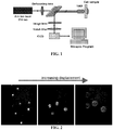
- FIGS. 2-6 The images and data presented in FIGS. 2-6 were recorded for nanocrystals that had been spin-coated onto a piece of smooth cover glass (RMS roughness ⁇ 1nm from atomic force microscope measurements).
- the ⁇ 514 nm line of an Ar-ion laser was used as the excitation source with a typical intensity of ⁇ 20W/cm 2 .
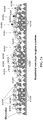
- FIG. 2 shows fluorescence microscope images of a field of nanocrystals at different values of z -displacement.
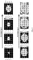
- FIG. 3 shows false color images of a single semiconductor nanocrystal at different values of z -displacement. The colors indicate intensity measured at the CCD detector.
- the fluorescence from each individual nanocrystal appears as a bright spot.
- complex ring patterns form due to the diffraction of the emission from each nanocrystal.
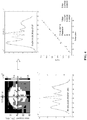
- FIG. 4 illustrates one method for determining the radius r 0 of the interference fringes.
- the radius r 0 is calculated as the distance between the peaks of the center and outermost Gaussian curves.
- more than one "slice” can be taken for each image.
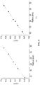
- the plot at lower right in FIG. 4 illustrates the linear correlation between r 0 and z displacement.
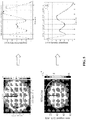
- FIG. 5 illustrates another method for determining r 0 .
- the integration of photon intensity as a function of angle ⁇ is plotted against the radial distance, and fitted to a multi-Gaussian function to calculate the center of the outermost ring, i.e., r 0 (fitting result shown as red curve).
- the measured correlation between r 0 and z -displacement is linear.
- a change in r 0 of -50 nm corresponds to a z -displacement of 90 nm.
- the resolution in z -displacement was approximately 8 nm, based the standard deviation of the measured ring sizes of several nanocrystals at the same image plane.
- the interpolation to zero radius for the FIG. 6A and FIG. 6B were 13.740 ⁇ m and 13.750 ⁇ m, respectively, a difference of 10 nm, consistent with nanocrystals having been deposited on a flat surface.
- FIG. 6C illustrate the mean and standard deviation of the measured positions of a single nanocrystal with repeated realizations of the image analysis.
- the difference between the means of the two displacements in FIG. 6C was 54 nm, as shown by the red line.
- the standard deviation around each mean, taken as a measure of the repeatability of the analysis procedure on noisy images, was 9 nm.
- Nanocrystal cores can be prepared by the pyrolysis of organometallic precursors in hot coordinating agents. See, for example, Murray, C.B., et al., J. Am. Chem. Soc. 1993, 115, 8706 , and Mikulec, F., Ph.D. Thesis, MIT, Cambridge, 1999 . Growth of shell layers on the bare nanocrystal cores can be carried out by simple modifications of conventional overcoating procedures. See, for example, Peng, X., et al., J. Am. Chem. Soc. 1997, 119, 7019 , Dabbousi, B.O., et al., J. Phys. Chem. B 1997, 101, 9463 , and Cao, Y. W. and Banin, U. Angew. Chem. Int. Edit. 1999, 38, 3692 .
- a coordinating agent can help control the growth of the nanocrystal.
- the coordinating agent is a compound having a donor lone pair that, for example, has a lone electron pair available to coordinate to a surface of the growing nanocrystal.
- the coordinating agent can be a solvent.
- a coordinating agent can stabilize the growing nanocrystal.
- Typical coordinating agents include alkyl phosphines, alkyl phosphine oxides, alkyl phosphonic acids, or alkyl phosphinic acids, however, other coordinating agents, such as pyridines, furans, and amines may also be suitable for the nanocrystal production. Examples of suitable coordinating agents include pyridine, tri-n-octyl phosphine (TOP) and tri-n-octyl phosphine oxide (TOPO). Technical grade TOPO can be used.
- the outer surface of the nanocrystal can include a layer of compounds derived from the coordinating agent used during the growth process.
- the surface can be modified by repeated exposure to an excess of a competing coordinating group to form an overlayer.
- a dispersion of nanocrystals capped with the coordinating agent used during growth can be treated with a coordinating organic compound, such as pyridine, to produce crystallites which disperse readily in pyridine, methanol, and aromatics but no longer disperse in aliphatic solvents.
- a surface exchange process can be carried out with any compound capable of coordinating to or bonding with the outer surface of the nanocrystal, including, for example, phosphines, thiols, amines and phosphates.
- the nanocrystal can be exposed to short chain polymers which exhibit an affinity for the surface and which terminate in a moiety having an affinity for a suspension or dispersion medium. Such affinity improves the stability of the suspension and discourages flocculation of the nanocrystal.
- Monodentate alkyl phosphines and alkyl phosphine oxides passivate nanocrystals efficiently.
- phosphine will refer to both phosphines and phosphine oxides below.
- Other conventional ligands such as thiols or phosphonic acids can be less effective than monodentate phosphines for maintaining the initial high nanocrystal luminescence over long periods. For example, the photoluminescence of nanocrystals consistently diminishes or quenches after ligand exchanges with thiols or phosphonic acid.
- Ligand exchanges can be carried out by one-phase or two-phase methods. Prior to ligand exchange, nanocrystals can be precipitated from their growth solutions by addition of methanol. The supernatant solution, which includes excess coordinating agent (e.g., trioctylphosphine), can be discarded. The precipitated nanocrystals can be redispersed in hexanes. Precipitation and redispersion can be repeated until essentially all the excess coordinating agent has been separated from the nanocrystals. A one-phase process can be used when both the nanocrystals and the ligands to be introduced are soluble in the same solvent. A solution with an excess of new ligands can be mixed with the nanocrystals.
- excess coordinating agent e.g., trioctylphosphine
- the mixture can be stirred at an elevated temperature until ligand exchange is complete.
- the one-phase method can be used, for example, to exchange octyl-modified oligomeric phosphines or methacrylate-modified oligomeric phosphines, which are both soluble in solvents that are compatible with the nanocrystals, such as hexanes.
- a two-phase ligand exchange process can be preferable when the nanocrystals and the new ligands do not have a common solvent.
- Nanocrystals can dissolved in an organic solvent such as dichloromethane, and the new ligand can be dissolved in an aqueous solution.
- the nanocrystals can be transferred from the organic phase to the aqueous phase by, for example, sonication.
- the transfer can be monitored through absorption and emission spectroscopy.
- a similar two-phase ligand exchange process has been reported earlier. See, for example, Wang, Y.A., et al., 2002 J. Am. Chem. Soc 124, 2293 .
- the nanocrystal can be a member of a population of nanocrystals having a narrow size distribution.
- the nanocrystal can be a sphere, rod, disk, or other shape.
- the nanocrystal can include a core of a semiconductor material.
- the nanocrystal can include a core having the formula MX, where M is cadmium, zinc, magnesium, mercury, aluminum, gallium, indium, thallium, or mixtures thereof, and X is oxygen, sulfur, selenium, tellurium, nitrogen, phosphorus, arsenic, antimony, or mixtures thereof.
- the semiconductor forming the core of the nanocrystal can include Group II-VI compounds, Group II-V compounds, Group III-VI compounds, Group III-V compounds, Group IV-VI compounds, Group I-III-VI compounds, Group II-IV-VI compounds, and Group II-IV-V compounds, for example, ZnS, ZnSe, ZnTe, CdS, CdSe, CdTe, HgS, HgSe, HgTe, AlN, AlP, AlAs, AlSb, GaN, GaP, GaAs, GaSb, GaSe, InN, InP, InAs, InSb, TIN, TIP, TIAs, TISb, PbS, PbSe, PbTe, or mixtures thereof.
- the core can have an overcoating on a surface of the core.
- the overcoating can be a semiconductor material having a composition different from the composition of the core.
- the overcoat of a semiconductor material on a surface of the nanocrystal can include a Group II-VI compounds, Group II-V compounds, Group III-VI compounds, Group III-V compounds, Group IV-VI compounds, Group I-III-VI compounds, Group II-IV-VI compounds, and Group II-IV-V compounds, for example, ZnS, ZnSe, ZnTe, CdS, CdSe, CdTe, HgS, HgSe, HgTe, AlN, AlP, AlAs, AlSb, GaN, GaP, GaAs, GaSb, GaSe, InN, InP, InAs, InSb, TIN, TIP, TIAs, TISb, PbS, PbSe, PbTe, or mixtures thereof.
- the overcoating material can have a band gap greater than the band gap of the core material.
- the overcoating material can have a band (i.e. the valence band or the conduction band) intermediate in energy to the valence and conduction bands of the core material. See for example, U.S. Patent Application Publication No. 20040110002 titled, "Semiconductor Nanocrystal Heterostructures".
- the emission from the nanocrystal can be a narrow Gaussian emission band that can be tuned through the complete wavelength range of the ultraviolet, visible, or infrared regions of the spectrum by varying the size of the nanocrystal, the composition of the nanocrystal, or both.
- CdSe can be tuned in the visible region
- InAs can be tuned in the infrared region.
- the population of nanocrystals can have a narrow size distribution.
- the population can be monodisperse and can exhibit less than a 15% rms deviation in diameter of the nanocrystals, preferably less than 10%, more preferably less than 5%.
- Spectral emissions in a narrow range of between 10 and 100 nm full width at half max (FWHM) can be observed.
- Semiconductor nanocrystals can have emission quantum efficiencies of greater than 2%, 5%, 10%, 20%, 40%, 60%, 70%, or 80%.
- Methods of preparing semiconductor nanocrystals include pyrolysis of organometallic reagents, such as dimethyl cadmium, injected into a hot, coordinating agent. This permits discrete nucleation and results in the controlled growth of macroscopic quantities of nanocrystals. Preparation and manipulation of nanocrystals are described, for example, in U.S. Patent No. 6,322,901 .
- the method of manufacturing a nanocrystal is a colloidal growth process and can produce a monodisperse particle population. Colloidal growth occurs by rapidly injecting an M donor and an X donor into a hot coordinating agent. The injection produces a nucleus that can be grown in a controlled manner to form a nanocrystal.
- the reaction mixture can be gently heated to grow and anneal the nanocrystal. Both the average size and the size distribution of the nanocrystals in a sample are dependent on the growth temperature. The growth temperature necessary to maintain steady growth increases with increasing average crystal size.
- the nanocrystal is a member of a population of nanocrystals. As a result of the discrete nucleation and controlled growth, the population of nanocrystals obtained has a narrow, monodisperse distribution of diameters. The monodisperse distribution of diameters can also be referred to as a size.
- the process of controlled growth and annealing of the nanocrystals in the coordinating agent that follows nucleation can also result in uniform surface derivatization and regular core structures. As the size distribution sharpens, the temperature can be raised to maintain steady growth. By adding more M donor or X donor, the growth period can be shortened.
- the M donor can be an inorganic compound, an organometallic compound, or elemental metal.
- the inorganic compound M-containing salt can be a metal halide, metal carboxylate, metal carbonate, metal hydroxide, or metal diketonate, such as a metal acetylacetonate. See, for example, U.S. Patent No. 6,576,291 .
- M is cadmium, zinc, magnesium, mercury, aluminum, gallium, indium or thallium.
- the X donor is a compound capable of reacting with the M donor to form a material with the general formula MX.
- the X donor is a chalcogenide donor or a pnictide donor, such as a phosphine chalcogenide, a bis(silyl) chalcogenide, dioxygen, an ammonium salt, or a tris(silyl) pnictide.
- a chalcogenide donor or a pnictide donor such as a phosphine chalcogenide, a bis(silyl) chalcogenide, dioxygen, an ammonium salt, or a tris(silyl) pnictide.
- Suitable X donors include dioxygen, bis(trimethylsilyl) selenide ((TMS) 2 Se), trialkyl phosphine selenides such as (tri-n-octylphosphine) selenide (TOPSe) or (tri-n-butylphosphine) selenide (TBPSe), trialkyl phosphine tellurides such as (tri-n-octylphosphine) telluride (TOPTe) or hexapropylphosphorustriamide telluride (HPPTTe), bis(trimethylsilyl)telluride ((TMS) 2 Te), bis(trimethylsilyl)sulfide ((TMS)2S), a trialkyl phosphine sulfide such as (tri-n-octylphosphine) sulfide (TOPS), an ammonium salt such as an ammonium halide (e.g., NH 4 Cl), tris(trimethyl
- Size distribution during the growth stage of the reaction can be estimated by monitoring the absorption line widths of the particles. Modification of the reaction temperature in response to changes in the absorption spectrum of the particles allows the maintenance of a sharp particle size distribution during growth. Reactants can be added to the nucleation solution during crystal growth to grow larger crystals. By stopping growth at a particular nanocrystal average diameter, a population having an average nanocrystal diameter of less than 150 ⁇ can be obtained. A population of nanocrystals can have an average diameter of 15 ⁇ to 125 ⁇ .
- the particle size distribution can be further refined by size selective precipitation with a poor solvent for the nanocrystals, such as methanol/butanol as described in U.S. Patent No. 6,322,901 .
- a poor solvent for the nanocrystals such as methanol/butanol as described in U.S. Patent No. 6,322,901 .
- nanocrystals can be dispersed in a solution of 10% butanol in hexane. Methanol can be added dropwise to this stirring solution until opalescence persists. Separation of supernatant and flocculate by centrifugation produces a precipitate enriched with the largest crystallites in the sample. This procedure can be repeated until no further sharpening of the optical absorption spectrum is noted.
- Size-selective precipitation can be carried out in a variety of solvent/nonsolvent pairs, including pyridine/hexane and chloroform/methanol.
- the size-selected nanocrystal population can have no more than a 15% rms deviation from mean diameter, preferably 10% rms deviation or less, and more preferably 5% rms deviation or less.
- the outer surface of the nanocrystal can include compounds derived from the coordinating solvent used during the growth process.
- the surface can be modified by repeated exposure to an excess of a competing coordinating group.
- a dispersion of the capped nanocrystal can be treated with a coordinating organic compound, such as pyridine, to produce crystallites which disperse readily in pyridine, methanol, and aromatics but no longer disperse in aliphatic solvents.
- a surface exchange process can be carried out with any compound capable of coordinating to or bonding with the outer surface of the nanocrystal, including, for example, phosphines, thiols, amines and phosphates.
- the nanocrystal can be exposed to short chain polymers which exhibit an affinity for the surface and which terminate in a moiety having an affinity for a suspension or dispersion medium. Such affinity improves the stability of the suspension and discourages flocculation of the nanocrystal.
- Nanocrystal coordinating compounds are described, for example, in U.S. Patent No. 6,251,303 .
- the coordinating ligand can have the formula: wherein k is 2, 3 or 5, and n is 1, 2, 3, 4 or 5 such that k-n is not less than zero;
- each of Y and L independently, is aryl, heteroaryl, or a straight or branched C 2-12 hydrocarbon chain optionally containing at least one double bond, at least one triple bond, or at least one double bond and one triple bond.
- the hydrocarbon chain can be optionally substituted with one or more C 1-4 alkyl, C 2-4 alkenyl, C 2-4 alkynyl, C 1-4 alkoxy, hydroxyl, halo, amino, nitro, cyano, C 3-5 cycloalkyl, 3-5 membered heterocycloalkyl, aryl, heteroaryl, C 1-4 alkylcarbonyloxy, C 1-4 alkyloxycarbonyl, C 1-4 alkylcarbonyl, or formyl.
- the hydrocarbon chain can also be optionally interrupted by -O-, -S-, -N(R a )-, -N(R a )-C(O)-O-, -O-C(O)-N(R a )-, -N(R a )-C(O)-N(R b )-, -O-C(O)-O-, -P(R a )-, or -P(O)(R a )-.
- R a and R b independently, is hydrogen, alkyl, alkenyl, alkynyl, alkoxy, hydroxylalkyl, hydroxyl, or haloalkyl.
- An aryl group is a substituted or unsubstituted cyclic aromatic group. Examples include phenyl, benzyl, naphthyl, tolyl, anthracyl, nitrophenyl, or halophenyl.
- a heteroaryl group is an aryl group with one or more heteroatoms in the ring, for instance furyl, pyiridyl, pyrrolyl, phenanthryl.
- a suitable coordinating ligand can be purchased commercially or prepared by ordinary synthetic organic techniques, for example, as described in J. March, Advanced Organic Chemistry .
- TEM Transmission electron microscopy
- Powder X-ray diffraction (XRD) patterns can provided the most complete information regarding the type and quality of the crystal structure of the nanocrystals.
- Estimates of size are also possible since particle diameter is inversely related, via the X-ray coherence length, to the peak width.
- the diameter of the nanocrystal can be measured directly by transmission electron microscopy or estimated from X-ray diffraction data using, for example, the Scherrer equation. It also can be estimated from the UV/Vis absorption spectrum.
- the ⁇ 514nm line of an Ar-ion laser was used as the excitation source with a typical intensity of -20 W/cm 2 . Images were taken using a 100x oil immersion objective (Nikon, Plan Apo) and an intensified CCD Camera (Pentamax, Princeton Instruments). The method used standard epifluorescence video imaging (as shown in FIG. 1 ) in off-focus mode and allows the tracking of particles with 100 ms temporal resolution.
- Primary bovine aortic endothelial cells (BAEC-77, passage 10-15) were cultured in DMEM supplemented with 10% fetal calf serum, 1% L-glutamine, and 1% penicillin-streptomycin. Before seeding, cell culture flasks and glass slides were coated with 0.2% gelatin at room temperature. Microfluidic chambers (from Ibidi) were coated with fibronectin to promote cell attachment in micro-environment. Cell cultures were kept in a humidified incubator maintained at 37 °C, with 5% CO 2 and 95% air.
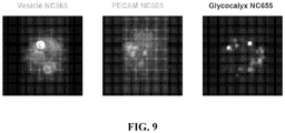
- NC655 nanocrystals coated with streptavidin were from Quantum Dot Corporation; NC605 nanocrystals coated with IgG were from Invitrogen; NC565 nanocrystals coated with PEG-OH were synthesized in lab.
- FIG. 7A After cell monolayers reached confluence, three layers of nanocrystals were attached to the cell as shown in FIG. 7A .
- Cells were incubated in culture medium with 5 nM NC565 for 15 min at 37 °C to allow the nanocrystals to be incorporated into intracellular vesicles via endocytosis.
- DPBS phosphate-HCl
- HSAG heparan sulfate glycosaminoglycans
- QD605 were added in a final concentration of 2 nM to stain platelet/endothelial cell adhesion molecule 1 (PECAM-1, same as CD31).
- PECAM-1 stain platelet/endothelial cell adhesion molecule 1
- NC565 prepared cell samples were transferred onto the nanopositioning stage (Physik Instrumente, P-527) and imaged immediately at room temperature.
- FIG. 7A is a schematic illustration of nanocrystal labeling of endothelial cells.
- Intracellular vesicles NC565, in green
- membrane PECAM-1 NC605, in orange
- glycocalyx NC655, in red
- NC565 were added in the growth medium to be taken up by cells through endocytocis
- NC605-IgG particles adhered to antibody attached PECAM molecules through IgG interaction
- NC655-streptavidin recognized biotin-coated heparin sulfate glycosaminoglycan antibody.
- the ring patterns indicate that vesicles (NC565) were the furthest from the scanning plane while the glycocalyx (NC655) was the closest to the scanning plane.
- the relative positions of the three layers from the data corroborated with the cell structure i.e., the glycocalyx being the outermost layer and the vesicles being located inside the cell.
- each nanocrystal After data processing, the precise location of each nanocrystal can be determined.
- the x,y location is calculated by a Gaussian fitting of the central spot, and z position from correlating the ring radius to the calibration curve.
- precise locations of seven vesicle-associated nanocrystals, eight PECAM-associated nanocrystals, and thirteen glycocalyx-associated nanocrystals, associated with a single cell were determined ( FIGS. 10A-10B ).
- the maximum z -distance between vesicle-associated nanocrystals and glycocalyx-associated nanocrystals was roughly 3.5 ⁇ m, on the same order as known cell body height.
- the thickness of the layer can be estimated by comparing the relative distance between the glycocalyx-associated nanocrystals and the membrane. Two possible approaches are discussed below.
- the glycocalyx thickness can be obtained directly from the z-difference of a glycocalyx-PECAM nanocrystal pair, assuming the membrane roughness between the two nanocrystals in the pair is negligible.
- a close examination of all the nanocrystals mapped ( FIGS. 10A-B ) revealed one glycocalyx-PECAM pair that satisfied the criteria.
- the z-difference between the two, ⁇ z 0.29 ⁇ m, provided an estimate of the glycocalyx thickness at this location.
- a second method involves assuming an ellipsoidal shape for the cell body, consistent with reported AFM measurements, and simulating a continuous surface of cell membrane by fitting the positions of eight PECAM-associated nanocrystals to an ellipsoidal surface as illustrated in FIG. 11 .
- the parameters of the ellipsoid fell within the physical range of cell geometry. Therefore, the z-distance of each individual glycocalyx-associated nanocrystal above membrane was calculated by comparing it to the z-position of the membrane right beneath the nanocrystal (i.e., at the same x,y position).
- the mean of the ⁇ z yielded an estimate of average glycocalyx thickness on the cell of 0.35 ⁇ 0.17 ⁇ m, which was on the same order of magnitude of the result from method 1.
- FIG. 13A shows an image recorded using the system of FIG. 12 .
- the time dependent x- and y -positions of the nanocrystal highlighted by the yellow arrow are shown in the graphs at right.
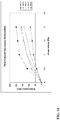
- FIG. 13B shows a detail of the y -position data, with the time trace of applied flow overlaid (orange line). Displacements of the nanocrystal closely match the applied flow. Average displacement was 108 ⁇ 77 nm.
- the applied shear stress was calculated to be 15 dyne/cm 2 , based on the fluid flow and chamber dimensions. Preliminary estimates of the shear modulus of the glycocalyx were in the range 3.7 Pa to 7.5 Pa. For comparison, the cell itself has a shear modulus on the order of 50 Pa to 600 Pa, depending on the method used.
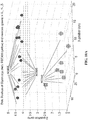
- FIG. 14 shows data illustrating the relationship between shear stress and nanocrystal displacement for five different nanocrystals. From this information, the shear modulus G for the glycocalyx was determined to be to be 6.7 ⁇ 3.3 Pa.
Landscapes
- Health & Medical Sciences (AREA)
- Chemical & Material Sciences (AREA)
- Life Sciences & Earth Sciences (AREA)
- Immunology (AREA)
- Physics & Mathematics (AREA)
- Engineering & Computer Science (AREA)
- General Physics & Mathematics (AREA)
- General Health & Medical Sciences (AREA)
- Biochemistry (AREA)
- Pathology (AREA)
- Analytical Chemistry (AREA)
- Nuclear Medicine, Radiotherapy & Molecular Imaging (AREA)
- Hematology (AREA)
- Urology & Nephrology (AREA)
- Molecular Biology (AREA)
- Biomedical Technology (AREA)
- Chemical Kinetics & Catalysis (AREA)
- Optics & Photonics (AREA)
- Crystallography & Structural Chemistry (AREA)
- Cell Biology (AREA)
- Biotechnology (AREA)
- Microbiology (AREA)
- Nanotechnology (AREA)
- Materials Engineering (AREA)
- Food Science & Technology (AREA)
- Medicinal Chemistry (AREA)
- Investigating, Analyzing Materials By Fluorescence Or Luminescence (AREA)
- Analysing Materials By The Use Of Radiation (AREA)
Claims (14)
- Verfahren zur Bildgebung eines mikroskopischen Objekts, das Folgendes umfasst:Anordnen eines mikroskopischen Objekts, das mit wenigstens einem ersten und einem zweiten Halbleiternanokristall assoziiert ist, in dem optischen Feld eines optischen Mikroskops; wobei wenigstens einer der Halbleiternanokristalle eine Affinität für eine biologische Struktur aufweist;Aufzeichnen eines ersten Fluoreszenzbildes des ersten und zweiten Halbleiternanokristalls bei einer ersten Fokustiefe;Aufzeichnen eines zweiten Fluoreszenzbildes des ersten und zweiten Halbleiternanokristalls bei einer zweiten Fokustiefe, die von der ersten Fokustiefe verschieden ist; undBerechnen der relativen Tiefen des ersten und zweiten Halbleiternanokristalls basierend wenigstens teilweise auf dem ersten und zweiten Fluoreszenzbild;wobei Berechnen der relativen Tiefen des ersten und zweiten Halbleiternanokristalls Messen eines Radius des ersten Halbleiternanokristalls, wie er in sowohl dem ersten als auch zweiten Fluoreszenzbild erscheint, beinhaltet;wobei das Messen des Radius Bestimmen eines radialen Intensitätsprofils bei jedem Radius durch Integrieren der Bildintensitäten als eine Funktion eines Winkels über alle Winkel, die den Umfang eines Kreises bei dem Radius definieren, und Bestimmen des äußersten Radius r0 aus dem radialen Intensitätsprofil beinhaltet.
- Verfahren nach Anspruch 1, das ferner Fitten des radialen Intensitätsprofils mit einer oder mehreren Gauß-Kurven umfasst.
- Verfahren nach Anspruch 1, das ferner Korrelieren des gemessenen Radius des ersten Halbleiternanokristalls mit der relativen Tiefe des ersten Halbleiternanokristalls umfasst.
- Verfahren nach Anspruch 1, das ferner Bestimmen relativer dreidimensionaler Koordinaten des ersten und zweiten Halbleiternanokristalls basierend wenigstens teilweise auf dem ersten und zweiten Fluoreszenzbild umfasst.
- Verfahren nach Anspruch 4, das ferner Bestimmen einer dreidimensionalen Form des Objekts basierend wenigstens teilweise auf den relativen dreidimensionalen Koordinaten des ersten und zweiten Halbleiternanokristalls umfasst.
- Verfahren nach Anspruch 1, wobei das Objekt eine biologische Struktur beinhaltet.
- Verfahren nach Anspruch 6, wobei der erste Halbleiternanokristall mit einer funktionalen Gruppe assoziiert ist, die eine spezielle Affinität für ein Biomolekül aufweist.
- Verfahren nach Anspruch 1, das ferner Verfolgen der Position wenigstens eines Halbleiternanokristalls als eine Funktion der Zeit umfasst.
- Verfahren nach Anspruch 6, wobei die biologische Struktur eine Zelle beinhaltet.
- Verfahren nach Anspruch 8, wobei das Verfolgen der Position Bestimmen dreidimensionaler Koordinaten für den Halbleiternanokristall beinhaltet.
- Verfahren zum Bestimmen der Position eines Nanokristalls in drei Dimensionen, das Folgendes umfasst:Aufzeichnen eines Fluoreszenzbildes eines Halbleiternanokristalls;Bestimmen von x- und y-Koordinaten von dem Zentrum des Nanokristallbildes; undBestimmen einer z-Koordinate aus dem Radius des Nanokristallbildes;wobei das Bestimmen der z-Koordinate aus dem Radius des Nanokristallbildes Bestimmen eines radialen Intensitätsprofils bei jedem Radius durch Integrieren der Bildintensität als eine Funktion eines Winkels über alle Winkel, die den Umfang eines Kreises bei dem Radius definieren, Bestimmen des äußersten Radius r0 aus dem radialen Intensitätsprofil und Bestimmen der z-Koordinate aus einer Korrelation der z-Koordinate gegenüber dem äußersten Radius r0 beinhaltet.
- Verfahren nach Anspruch 11, wobei die x-, y- und z-Koordinaten jeweils individuell eine Genauigkeit von ±15 nm oder weniger aufweisen.
- Verfahren nach Anspruch 11, wobei die x-, y- und z-Koordinaten jeweils individuell eine Genauigkeit von ±10 nm oder weniger aufweisen.
- Verfahren nach Anspruch 11, das ferner Fitten des radialen Intensitätsprofils mit einer oder mehreren Gauß-Kurven umfasst.
Applications Claiming Priority (2)
| Application Number | Priority Date | Filing Date | Title |
|---|---|---|---|
| US97531907P | 2007-09-26 | 2007-09-26 | |
| PCT/US2008/077874 WO2009082523A2 (en) | 2007-09-26 | 2008-09-26 | High-resolution 3d imaging of single semiconductor nanocrystals |
Publications (3)
| Publication Number | Publication Date |
|---|---|
| EP2193468A2 EP2193468A2 (de) | 2010-06-09 |
| EP2193468A4 EP2193468A4 (de) | 2017-08-09 |
| EP2193468B1 true EP2193468B1 (de) | 2019-03-27 |
Family
ID=40801734
Family Applications (1)
| Application Number | Title | Priority Date | Filing Date |
|---|---|---|---|
| EP08865911.5A Active EP2193468B1 (de) | 2007-09-26 | 2008-09-26 | 3d-abbildung einzelner halbleiternanokristalle mit hoher auflösung |
Country Status (4)
| Country | Link |
|---|---|
| US (1) | US8947516B2 (de) |
| EP (1) | EP2193468B1 (de) |
| JP (1) | JP2010540939A (de) |
| WO (1) | WO2009082523A2 (de) |
Families Citing this family (10)
| Publication number | Priority date | Publication date | Assignee | Title |
|---|---|---|---|---|
| CN102713720B (zh) | 2009-10-28 | 2016-05-11 | 阿兰蒂克微科学股份有限公司 | 显微成像装置和显微成像方法 |
| US9075225B2 (en) | 2009-10-28 | 2015-07-07 | Alentic Microscience Inc. | Microscopy imaging |
| US20140152801A1 (en) | 2009-10-28 | 2014-06-05 | Alentic Microscience Inc. | Detecting and Using Light Representative of a Sample |
| JP5928308B2 (ja) * | 2012-11-13 | 2016-06-01 | ソニー株式会社 | 画像取得装置および画像取得方法 |
| US9063434B2 (en) | 2013-01-11 | 2015-06-23 | University Of Utah Research Foundation | Sub-diffraction-limited patterning and imaging via multi-step photoswitching |
| US10502666B2 (en) | 2013-02-06 | 2019-12-10 | Alentic Microscience Inc. | Sample processing improvements for quantitative microscopy |
| JP2016531282A (ja) | 2013-06-26 | 2016-10-06 | アレンティック マイクロサイエンス インコーポレイテッド | 顕微鏡法に関するサンプル処理の改善 |
| CN103606181A (zh) * | 2013-10-16 | 2014-02-26 | 北京航空航天大学 | 一种显微三维重构方法 |
| JP6504160B2 (ja) * | 2014-04-21 | 2019-04-24 | コニカミノルタ株式会社 | 生体物質定量方法、画像処理装置、病理診断支援システム及び画像処理プログラム |
| US11423533B2 (en) * | 2016-12-27 | 2022-08-23 | Konica Minolta, Inc. | Image processing method and image processing system |
Family Cites Families (29)
| Publication number | Priority date | Publication date | Assignee | Title |
|---|---|---|---|---|
| JPH07286953A (ja) * | 1994-04-19 | 1995-10-31 | Toa Medical Electronics Co Ltd | イメージングフローサイトメータ |
| JPH097196A (ja) * | 1995-06-20 | 1997-01-10 | Matsushita Electric Ind Co Ltd | 光ヘッドの調整方法 |
| US6322901B1 (en) * | 1997-11-13 | 2001-11-27 | Massachusetts Institute Of Technology | Highly luminescent color-selective nano-crystalline materials |
| US6207392B1 (en) * | 1997-11-25 | 2001-03-27 | The Regents Of The University Of California | Semiconductor nanocrystal probes for biological applications and process for making and using such probes |
| US6251303B1 (en) * | 1998-09-18 | 2001-06-26 | Massachusetts Institute Of Technology | Water-soluble fluorescent nanocrystals |
| US6306610B1 (en) * | 1998-09-18 | 2001-10-23 | Massachusetts Institute Of Technology | Biological applications of quantum dots |
| ATE362615T1 (de) * | 2000-03-20 | 2007-06-15 | Massachusetts Inst Technology | Anorganische teilchenkonjugate |
| US6759235B2 (en) * | 2000-04-06 | 2004-07-06 | Quantum Dot Corporation | Two-dimensional spectral imaging system |
| US6844150B2 (en) * | 2000-08-24 | 2005-01-18 | The Regents Of The University Of California | Ultrahigh resolution multicolor colocalization of single fluorescent probes |
| US6576291B2 (en) * | 2000-12-08 | 2003-06-10 | Massachusetts Institute Of Technology | Preparation of nanocrystallites |
| AU2002326920B2 (en) * | 2001-09-17 | 2007-09-13 | Massachusetts Institute Of Technology | Semiconductor nanocrystal composite |
| ATE399990T1 (de) * | 2001-10-09 | 2008-07-15 | Univ Ruprecht Karls Heidelberg | Fernfeld lichtmikroskopische methode und vorrichtung zur bestimmung von mindestens einem objekt kleiner als die benutzte wellenlänge |
| WO2003038401A2 (en) * | 2001-10-31 | 2003-05-08 | The Regents Of The University Of California | Semiconductor nanocrystal-based cellular imaging |
| US6770892B2 (en) * | 2002-02-28 | 2004-08-03 | Agilent Technologies, Inc. | Method and system for automated focus-distance determination for molecular array scanners |
| US6835938B2 (en) * | 2002-07-31 | 2004-12-28 | Agilent Technologies, Inc. | Biopolymer array substrate thickness dependent automated focus-distance determination method for biopolymer array scanners |
| EP2336409B1 (de) * | 2002-08-13 | 2023-05-10 | Massachusetts Institute of Technology | Beschichteter Nanokristall und Verfahren zur Herstellung eines beschichteten Nanokristalles |
| EP1576655B1 (de) * | 2002-08-15 | 2014-05-21 | Moungi G. Bawendi | Stabilisierte halbleiternanokristalle |
| US7468518B2 (en) * | 2003-10-23 | 2008-12-23 | National University Of Singapore | Fluorescence correlation spectroscopy with single excitation wavelength |
| EP1682878A1 (de) * | 2003-10-31 | 2006-07-26 | Art Advanced Research Technologies Inc. | Zeitdomänenverfahren und vorrichtung zur bestimmung der tiefe und konzentration eines fluorophors in einem trüben medium |
| US7075097B2 (en) * | 2004-03-25 | 2006-07-11 | Mitutoyo Corporation | Optical path array and angular filter for translation and orientation sensing |
| US7229690B2 (en) * | 2004-07-26 | 2007-06-12 | Massachusetts Institute Of Technology | Microspheres including nanoparticles |
| WO2006033732A1 (en) * | 2004-08-17 | 2006-03-30 | Invitrogen Corporation | Synthesis of highly luminescent colloidal particles |
| WO2007001438A2 (en) * | 2004-10-29 | 2007-01-04 | Molecular Probes, Inc. | Functionalized fluorescent nanocrystals, and methods for their preparation and use |
| EP2453238B1 (de) * | 2005-05-23 | 2016-12-21 | Harald F. Hess | Optische Mikroskopie mit phototransformierbaren optischen Markern |
| US9089619B2 (en) * | 2005-06-06 | 2015-07-28 | University Of Kentucky | Hybrid nanocrystals for treatment and bioimaging of disease |
| US8785505B2 (en) * | 2005-10-28 | 2014-07-22 | The Regents Of The University Of California | Toxicology and cellular effect of manufactured nanomaterials |
| US7817841B2 (en) * | 2005-11-12 | 2010-10-19 | General Electric Company | Time-lapse cell cycle analysis of unstained nuclei |
| JP4572162B2 (ja) * | 2005-11-22 | 2010-10-27 | 株式会社ジーオングストローム | 顕微鏡装置 |
| EP2165185B1 (de) * | 2007-06-26 | 2015-08-19 | Massachusetts Institute of Technology | Kontrollierte modifikation von halbleiter-nanokristallen |
-
2008
- 2008-09-26 WO PCT/US2008/077874 patent/WO2009082523A2/en not_active Ceased
- 2008-09-26 EP EP08865911.5A patent/EP2193468B1/de active Active
- 2008-09-26 JP JP2010527186A patent/JP2010540939A/ja active Pending
- 2008-09-26 US US12/680,150 patent/US8947516B2/en active Active
Non-Patent Citations (1)
| Title |
|---|
| None * |
Also Published As
| Publication number | Publication date |
|---|---|
| US20110037846A1 (en) | 2011-02-17 |
| US8947516B2 (en) | 2015-02-03 |
| WO2009082523A3 (en) | 2010-05-14 |
| EP2193468A2 (de) | 2010-06-09 |
| EP2193468A4 (de) | 2017-08-09 |
| JP2010540939A (ja) | 2010-12-24 |
| WO2009082523A2 (en) | 2009-07-02 |
Similar Documents
| Publication | Publication Date | Title |
|---|---|---|
| EP2193468B1 (de) | 3d-abbildung einzelner halbleiternanokristalle mit hoher auflösung | |
| US10084042B2 (en) | Nanocrystals with high extinction coefficients and methods of making and using such nanocrystals | |
| KR101586875B1 (ko) | 안정한 나노 입자 및 이러한 입자의 제조 및 사용 방법 | |
| US8889414B2 (en) | Semiconductor nanocrystal-based phagokinetic tracking | |
| Jorge et al. | Optical fiber sensing using quantum dots | |
| US20140206096A1 (en) | Stable indium-containing semiconductor nanocrystals | |
| KR20180005164A (ko) | 지속 발광성 코어/쉘 나노플레이트렛 | |
| Pompa et al. | Fluorescence enhancement in colloidal semiconductor nanocrystals by metallic nanopatterns | |
| WO2006014576A2 (en) | Fluorescent lifetime biological detection and imaging using water-stable semiconductor nanocrystals | |
| Wang et al. | Effective improvement in optical properties of colloidal CdTe@ ZnS quantum dots synthesized from aqueous solution | |
| Santos et al. | Semiconductor quantum dots for biological applications | |
| Pierce et al. | Applications of quantum dots in bioimaging and bioassays | |
| Knight et al. | Evaluation of the suitability of quantum dots as fluorescence standards. | |
| Chomoucká et al. | Synthesis and modification of quantum dots for medical applications | |
| 増田志穂美 | Establishment of LSPR-mediated fluorescence imaging for cell-attached nanointerface | |
| Bokhari | Confocal Imaging and Analysis of Quantum Dots on living Cells | |
| Lu | Some studies of nanocrystal quantum dots on chemically functionalized substrates (semiconductors) for novel biological sensing | |
| Zhang et al. | Hyperspectral Microscopy and Cellular Array Imaging Using Colloidal Quantum Dots | |
| Oldenburg et al. | Optically detectable colloidal metal labels: properties, methods, and biomedical applications | |
| Özdemir | Production and characterization of water soluble CdSeTe based core/shell nanocrystals and their applications in bioimaging | |
| CA2573150A1 (en) | Fluorescent lifetime biological detection and imaging using water-stable semiconductor nanocrystals |
Legal Events
| Date | Code | Title | Description |
|---|---|---|---|
| PUAI | Public reference made under article 153(3) epc to a published international application that has entered the european phase |
Free format text: ORIGINAL CODE: 0009012 |
|
| 17P | Request for examination filed |
Effective date: 20100330 |
|
| AK | Designated contracting states |
Kind code of ref document: A2 Designated state(s): AT BE BG CH CY CZ DE DK EE ES FI FR GB GR HR HU IE IS IT LI LT LU LV MC MT NL NO PL PT RO SE SI SK TR |
|
| AX | Request for extension of the european patent |
Extension state: AL BA MK RS |
|
| R17D | Deferred search report published (corrected) |
Effective date: 20100514 |
|
| RIN1 | Information on inventor provided before grant (corrected) |
Inventor name: BAWENDI, MOUNGI G. Inventor name: DEWEY, C. FORBES Inventor name: YAO, YU Inventor name: HUANG, HAO |
|
| DAX | Request for extension of the european patent (deleted) | ||
| REG | Reference to a national code |
Ref country code: DE Ref legal event code: R079 Ref document number: 602008059541 Country of ref document: DE Free format text: PREVIOUS MAIN CLASS: G06F0019000000 Ipc: G01N0021640000 |
|
| A4 | Supplementary search report drawn up and despatched |
Effective date: 20170712 |
|
| RIC1 | Information provided on ipc code assigned before grant |
Ipc: G06F 19/00 20110101ALI20170706BHEP Ipc: G01N 33/533 20060101ALI20170706BHEP Ipc: G01N 21/64 20060101AFI20170706BHEP Ipc: G01N 33/58 20060101ALI20170706BHEP Ipc: A61K 49/00 20060101ALI20170706BHEP Ipc: B82Y 15/00 20110101ALI20170706BHEP |
|
| GRAP | Despatch of communication of intention to grant a patent |
Free format text: ORIGINAL CODE: EPIDOSNIGR1 |
|
| STAA | Information on the status of an ep patent application or granted ep patent |
Free format text: STATUS: GRANT OF PATENT IS INTENDED |
|
| INTG | Intention to grant announced |
Effective date: 20181002 |
|
| GRAS | Grant fee paid |
Free format text: ORIGINAL CODE: EPIDOSNIGR3 |
|
| GRAA | (expected) grant |
Free format text: ORIGINAL CODE: 0009210 |
|
| STAA | Information on the status of an ep patent application or granted ep patent |
Free format text: STATUS: THE PATENT HAS BEEN GRANTED |
|
| AK | Designated contracting states |
Kind code of ref document: B1 Designated state(s): AT BE BG CH CY CZ DE DK EE ES FI FR GB GR HR HU IE IS IT LI LT LU LV MC MT NL NO PL PT RO SE SI SK TR |
|
| REG | Reference to a national code |
Ref country code: GB Ref legal event code: FG4D |
|
| REG | Reference to a national code |
Ref country code: CH Ref legal event code: EP |
|
| REG | Reference to a national code |
Ref country code: AT Ref legal event code: REF Ref document number: 1113694 Country of ref document: AT Kind code of ref document: T Effective date: 20190415 |
|
| REG | Reference to a national code |
Ref country code: IE Ref legal event code: FG4D |
|
| REG | Reference to a national code |
Ref country code: DE Ref legal event code: R096 Ref document number: 602008059541 Country of ref document: DE |
|
| PG25 | Lapsed in a contracting state [announced via postgrant information from national office to epo] |
Ref country code: FI Free format text: LAPSE BECAUSE OF FAILURE TO SUBMIT A TRANSLATION OF THE DESCRIPTION OR TO PAY THE FEE WITHIN THE PRESCRIBED TIME-LIMIT Effective date: 20190327 Ref country code: LT Free format text: LAPSE BECAUSE OF FAILURE TO SUBMIT A TRANSLATION OF THE DESCRIPTION OR TO PAY THE FEE WITHIN THE PRESCRIBED TIME-LIMIT Effective date: 20190327 Ref country code: NO Free format text: LAPSE BECAUSE OF FAILURE TO SUBMIT A TRANSLATION OF THE DESCRIPTION OR TO PAY THE FEE WITHIN THE PRESCRIBED TIME-LIMIT Effective date: 20190627 Ref country code: SE Free format text: LAPSE BECAUSE OF FAILURE TO SUBMIT A TRANSLATION OF THE DESCRIPTION OR TO PAY THE FEE WITHIN THE PRESCRIBED TIME-LIMIT Effective date: 20190327 |
|
| REG | Reference to a national code |
Ref country code: NL Ref legal event code: MP Effective date: 20190327 |
|
| PG25 | Lapsed in a contracting state [announced via postgrant information from national office to epo] |
Ref country code: HR Free format text: LAPSE BECAUSE OF FAILURE TO SUBMIT A TRANSLATION OF THE DESCRIPTION OR TO PAY THE FEE WITHIN THE PRESCRIBED TIME-LIMIT Effective date: 20190327 Ref country code: LV Free format text: LAPSE BECAUSE OF FAILURE TO SUBMIT A TRANSLATION OF THE DESCRIPTION OR TO PAY THE FEE WITHIN THE PRESCRIBED TIME-LIMIT Effective date: 20190327 Ref country code: GR Free format text: LAPSE BECAUSE OF FAILURE TO SUBMIT A TRANSLATION OF THE DESCRIPTION OR TO PAY THE FEE WITHIN THE PRESCRIBED TIME-LIMIT Effective date: 20190628 Ref country code: BG Free format text: LAPSE BECAUSE OF FAILURE TO SUBMIT A TRANSLATION OF THE DESCRIPTION OR TO PAY THE FEE WITHIN THE PRESCRIBED TIME-LIMIT Effective date: 20190627 Ref country code: NL Free format text: LAPSE BECAUSE OF FAILURE TO SUBMIT A TRANSLATION OF THE DESCRIPTION OR TO PAY THE FEE WITHIN THE PRESCRIBED TIME-LIMIT Effective date: 20190327 |
|
| REG | Reference to a national code |
Ref country code: AT Ref legal event code: MK05 Ref document number: 1113694 Country of ref document: AT Kind code of ref document: T Effective date: 20190327 |
|
| PG25 | Lapsed in a contracting state [announced via postgrant information from national office to epo] |
Ref country code: ES Free format text: LAPSE BECAUSE OF FAILURE TO SUBMIT A TRANSLATION OF THE DESCRIPTION OR TO PAY THE FEE WITHIN THE PRESCRIBED TIME-LIMIT Effective date: 20190327 Ref country code: PT Free format text: LAPSE BECAUSE OF FAILURE TO SUBMIT A TRANSLATION OF THE DESCRIPTION OR TO PAY THE FEE WITHIN THE PRESCRIBED TIME-LIMIT Effective date: 20190727 Ref country code: SK Free format text: LAPSE BECAUSE OF FAILURE TO SUBMIT A TRANSLATION OF THE DESCRIPTION OR TO PAY THE FEE WITHIN THE PRESCRIBED TIME-LIMIT Effective date: 20190327 Ref country code: CZ Free format text: LAPSE BECAUSE OF FAILURE TO SUBMIT A TRANSLATION OF THE DESCRIPTION OR TO PAY THE FEE WITHIN THE PRESCRIBED TIME-LIMIT Effective date: 20190327 Ref country code: RO Free format text: LAPSE BECAUSE OF FAILURE TO SUBMIT A TRANSLATION OF THE DESCRIPTION OR TO PAY THE FEE WITHIN THE PRESCRIBED TIME-LIMIT Effective date: 20190327 Ref country code: EE Free format text: LAPSE BECAUSE OF FAILURE TO SUBMIT A TRANSLATION OF THE DESCRIPTION OR TO PAY THE FEE WITHIN THE PRESCRIBED TIME-LIMIT Effective date: 20190327 Ref country code: IT Free format text: LAPSE BECAUSE OF FAILURE TO SUBMIT A TRANSLATION OF THE DESCRIPTION OR TO PAY THE FEE WITHIN THE PRESCRIBED TIME-LIMIT Effective date: 20190327 |
|
| PG25 | Lapsed in a contracting state [announced via postgrant information from national office to epo] |
Ref country code: PL Free format text: LAPSE BECAUSE OF FAILURE TO SUBMIT A TRANSLATION OF THE DESCRIPTION OR TO PAY THE FEE WITHIN THE PRESCRIBED TIME-LIMIT Effective date: 20190327 |
|
| PG25 | Lapsed in a contracting state [announced via postgrant information from national office to epo] |
Ref country code: IS Free format text: LAPSE BECAUSE OF FAILURE TO SUBMIT A TRANSLATION OF THE DESCRIPTION OR TO PAY THE FEE WITHIN THE PRESCRIBED TIME-LIMIT Effective date: 20190727 Ref country code: AT Free format text: LAPSE BECAUSE OF FAILURE TO SUBMIT A TRANSLATION OF THE DESCRIPTION OR TO PAY THE FEE WITHIN THE PRESCRIBED TIME-LIMIT Effective date: 20190327 |
|
| REG | Reference to a national code |
Ref country code: DE Ref legal event code: R097 Ref document number: 602008059541 Country of ref document: DE |
|
| PG25 | Lapsed in a contracting state [announced via postgrant information from national office to epo] |
Ref country code: DK Free format text: LAPSE BECAUSE OF FAILURE TO SUBMIT A TRANSLATION OF THE DESCRIPTION OR TO PAY THE FEE WITHIN THE PRESCRIBED TIME-LIMIT Effective date: 20190327 |
|
| PLBE | No opposition filed within time limit |
Free format text: ORIGINAL CODE: 0009261 |
|
| STAA | Information on the status of an ep patent application or granted ep patent |
Free format text: STATUS: NO OPPOSITION FILED WITHIN TIME LIMIT |
|
| PG25 | Lapsed in a contracting state [announced via postgrant information from national office to epo] |
Ref country code: SI Free format text: LAPSE BECAUSE OF FAILURE TO SUBMIT A TRANSLATION OF THE DESCRIPTION OR TO PAY THE FEE WITHIN THE PRESCRIBED TIME-LIMIT Effective date: 20190327 |
|
| 26N | No opposition filed |
Effective date: 20200103 |
|
| PG25 | Lapsed in a contracting state [announced via postgrant information from national office to epo] |
Ref country code: TR Free format text: LAPSE BECAUSE OF FAILURE TO SUBMIT A TRANSLATION OF THE DESCRIPTION OR TO PAY THE FEE WITHIN THE PRESCRIBED TIME-LIMIT Effective date: 20190327 |
|
| PG25 | Lapsed in a contracting state [announced via postgrant information from national office to epo] |
Ref country code: MC Free format text: LAPSE BECAUSE OF FAILURE TO SUBMIT A TRANSLATION OF THE DESCRIPTION OR TO PAY THE FEE WITHIN THE PRESCRIBED TIME-LIMIT Effective date: 20190327 |
|
| REG | Reference to a national code |
Ref country code: CH Ref legal event code: PL |
|
| PG25 | Lapsed in a contracting state [announced via postgrant information from national office to epo] |
Ref country code: LU Free format text: LAPSE BECAUSE OF NON-PAYMENT OF DUE FEES Effective date: 20190926 Ref country code: IE Free format text: LAPSE BECAUSE OF NON-PAYMENT OF DUE FEES Effective date: 20190926 Ref country code: CH Free format text: LAPSE BECAUSE OF NON-PAYMENT OF DUE FEES Effective date: 20190930 Ref country code: LI Free format text: LAPSE BECAUSE OF NON-PAYMENT OF DUE FEES Effective date: 20190930 |
|
| REG | Reference to a national code |
Ref country code: BE Ref legal event code: MM Effective date: 20190930 |
|
| PG25 | Lapsed in a contracting state [announced via postgrant information from national office to epo] |
Ref country code: BE Free format text: LAPSE BECAUSE OF NON-PAYMENT OF DUE FEES Effective date: 20190930 |
|
| PG25 | Lapsed in a contracting state [announced via postgrant information from national office to epo] |
Ref country code: CY Free format text: LAPSE BECAUSE OF FAILURE TO SUBMIT A TRANSLATION OF THE DESCRIPTION OR TO PAY THE FEE WITHIN THE PRESCRIBED TIME-LIMIT Effective date: 20190327 |
|
| PG25 | Lapsed in a contracting state [announced via postgrant information from national office to epo] |
Ref country code: MT Free format text: LAPSE BECAUSE OF FAILURE TO SUBMIT A TRANSLATION OF THE DESCRIPTION OR TO PAY THE FEE WITHIN THE PRESCRIBED TIME-LIMIT Effective date: 20190327 Ref country code: HU Free format text: LAPSE BECAUSE OF FAILURE TO SUBMIT A TRANSLATION OF THE DESCRIPTION OR TO PAY THE FEE WITHIN THE PRESCRIBED TIME-LIMIT; INVALID AB INITIO Effective date: 20080926 |
|
| P01 | Opt-out of the competence of the unified patent court (upc) registered |
Effective date: 20230528 |
|
| PGFP | Annual fee paid to national office [announced via postgrant information from national office to epo] |
Ref country code: DE Payment date: 20250929 Year of fee payment: 18 |
|
| PGFP | Annual fee paid to national office [announced via postgrant information from national office to epo] |
Ref country code: GB Payment date: 20250929 Year of fee payment: 18 |
|
| PGFP | Annual fee paid to national office [announced via postgrant information from national office to epo] |
Ref country code: FR Payment date: 20250925 Year of fee payment: 18 |