EP2197042A2 - Cellule solaire dotée d'une diode de dérivation à croissance monolithe intégrale - Google Patents
Cellule solaire dotée d'une diode de dérivation à croissance monolithe intégrale Download PDFInfo
- Publication number
- EP2197042A2 EP2197042A2 EP09014641A EP09014641A EP2197042A2 EP 2197042 A2 EP2197042 A2 EP 2197042A2 EP 09014641 A EP09014641 A EP 09014641A EP 09014641 A EP09014641 A EP 09014641A EP 2197042 A2 EP2197042 A2 EP 2197042A2
- Authority
- EP
- European Patent Office
- Prior art keywords
- solar cell
- contact
- cell
- layers
- region
- Prior art date
- Legal status (The legal status is an assumption and is not a legal conclusion. Google has not performed a legal analysis and makes no representation as to the accuracy of the status listed.)
- Withdrawn
Links
Images


Classifications
-
- H—ELECTRICITY
- H10—SEMICONDUCTOR DEVICES; ELECTRIC SOLID-STATE DEVICES NOT OTHERWISE PROVIDED FOR
- H10F—INORGANIC SEMICONDUCTOR DEVICES SENSITIVE TO INFRARED RADIATION, LIGHT, ELECTROMAGNETIC RADIATION OF SHORTER WAVELENGTH OR CORPUSCULAR RADIATION
- H10F10/00—Individual photovoltaic cells, e.g. solar cells
- H10F10/10—Individual photovoltaic cells, e.g. solar cells having potential barriers
- H10F10/14—Photovoltaic cells having only PN homojunction potential barriers
- H10F10/142—Photovoltaic cells having only PN homojunction potential barriers comprising multiple PN homojunctions, e.g. tandem cells
-
- H—ELECTRICITY
- H10—SEMICONDUCTOR DEVICES; ELECTRIC SOLID-STATE DEVICES NOT OTHERWISE PROVIDED FOR
- H10F—INORGANIC SEMICONDUCTOR DEVICES SENSITIVE TO INFRARED RADIATION, LIGHT, ELECTROMAGNETIC RADIATION OF SHORTER WAVELENGTH OR CORPUSCULAR RADIATION
- H10F19/00—Integrated devices, or assemblies of multiple devices, comprising at least one photovoltaic cell covered by group H10F10/00, e.g. photovoltaic modules
- H10F19/20—Integrated devices, or assemblies of multiple devices, comprising at least one photovoltaic cell covered by group H10F10/00, e.g. photovoltaic modules comprising photovoltaic cells in arrays in or on a single semiconductor substrate, the photovoltaic cells having planar junctions
-
- H—ELECTRICITY
- H10—SEMICONDUCTOR DEVICES; ELECTRIC SOLID-STATE DEVICES NOT OTHERWISE PROVIDED FOR
- H10F—INORGANIC SEMICONDUCTOR DEVICES SENSITIVE TO INFRARED RADIATION, LIGHT, ELECTROMAGNETIC RADIATION OF SHORTER WAVELENGTH OR CORPUSCULAR RADIATION
- H10F19/00—Integrated devices, or assemblies of multiple devices, comprising at least one photovoltaic cell covered by group H10F10/00, e.g. photovoltaic modules
- H10F19/70—Integrated devices, or assemblies of multiple devices, comprising at least one photovoltaic cell covered by group H10F10/00, e.g. photovoltaic modules comprising bypass diodes
- H10F19/75—Integrated devices, or assemblies of multiple devices, comprising at least one photovoltaic cell covered by group H10F10/00, e.g. photovoltaic modules comprising bypass diodes the bypass diodes being integrated or directly associated with the photovoltaic cells, e.g. formed in or on the same substrate
-
- H—ELECTRICITY
- H10—SEMICONDUCTOR DEVICES; ELECTRIC SOLID-STATE DEVICES NOT OTHERWISE PROVIDED FOR
- H10W—GENERIC PACKAGES, INTERCONNECTIONS, CONNECTORS OR OTHER CONSTRUCTIONAL DETAILS OF DEVICES COVERED BY CLASS H10
- H10W90/00—Package configurations
- H10W90/701—Package configurations characterised by the relative positions of pads or connectors relative to package parts
- H10W90/751—Package configurations characterised by the relative positions of pads or connectors relative to package parts of bond wires
- H10W90/753—Package configurations characterised by the relative positions of pads or connectors relative to package parts of bond wires between laterally-adjacent chips
-
- Y—GENERAL TAGGING OF NEW TECHNOLOGICAL DEVELOPMENTS; GENERAL TAGGING OF CROSS-SECTIONAL TECHNOLOGIES SPANNING OVER SEVERAL SECTIONS OF THE IPC; TECHNICAL SUBJECTS COVERED BY FORMER USPC CROSS-REFERENCE ART COLLECTIONS [XRACs] AND DIGESTS
- Y02—TECHNOLOGIES OR APPLICATIONS FOR MITIGATION OR ADAPTATION AGAINST CLIMATE CHANGE
- Y02E—REDUCTION OF GREENHOUSE GAS [GHG] EMISSIONS, RELATED TO ENERGY GENERATION, TRANSMISSION OR DISTRIBUTION
- Y02E10/00—Energy generation through renewable energy sources
- Y02E10/50—Photovoltaic [PV] energy
- Y02E10/544—Solar cells from Group III-V materials
-
- Y—GENERAL TAGGING OF NEW TECHNOLOGICAL DEVELOPMENTS; GENERAL TAGGING OF CROSS-SECTIONAL TECHNOLOGIES SPANNING OVER SEVERAL SECTIONS OF THE IPC; TECHNICAL SUBJECTS COVERED BY FORMER USPC CROSS-REFERENCE ART COLLECTIONS [XRACs] AND DIGESTS
- Y02—TECHNOLOGIES OR APPLICATIONS FOR MITIGATION OR ADAPTATION AGAINST CLIMATE CHANGE
- Y02E—REDUCTION OF GREENHOUSE GAS [GHG] EMISSIONS, RELATED TO ENERGY GENERATION, TRANSMISSION OR DISTRIBUTION
- Y02E10/00—Energy generation through renewable energy sources
- Y02E10/50—Photovoltaic [PV] energy
- Y02E10/547—Monocrystalline silicon PV cells
Definitions
- the present invention relates to solar cells.
- the present invention relates to methods and apparatuses for providing a solar cell with an integral diode.
- Photovoltaic cells are well-known devices which convert solar energy into electrical energy. Solar cells have long been used to generate electrical power in both terrestrial and space applications. Solar cells offer several advantages over more conventional power sources. For example, solar cells offer a clean method for generating electricity. Furthermore, solar cells do not have to be replenished with fossil fuels. Instead, solar cells are powered by the virtually limitless energy of the sun. However, the use of solar cells has been limited because solar cells are a relatively expensive method of generating electricity. Nonetheless, the solar cell is an attractive device for generating energy in space, where low-cost conventional power sources are unavailable.
- Solar cells are typically assembled into arrays of solar cells connected together in series, or in parallel, or in a series-parallel combination.
- the desired output voltage and current at least in part, determine the number of cells in an array, as well as the array topology.
- each cell when all cells in an array are illuminated, each cell will be forward biased. However, if one or more of the cells is shadowed (i.e., not illuminated), by a satellite antenna or the like, the shadowed cell or cells may become reversed biased because of the voltage generated by the unshadowed cells. Reverse biasing of a cell can cause permanent degradation in cell performance or even complete cell failure. To guard against such damage, it is customary to provide protective bypass diodes. One bypass diode may be connected across several cells, or for enhanced reliability, each cell may have its own bypass diode. Multijunction solar cells are particularly susceptible to damage when subjected to a reverse bias condition. Thus, multijunction cells in particular benefit from having one bypass diode per cell.
- a bypass diode is connected in an anti-parallel configuration, with the anode and the cathode of the bypass diode respectively connected to the cathode and the anode of the solar cell, so that the bypass diode will be reversed biased when the cells are illuminated.
- the bypass diode connected across the shadowed cell in turn becomes forward biased. Most of the current will flow through the bypass diode rather than through the shadowed cell, thereby allowing current to continue flowing through the array.
- the bypass diode limits the reverse bias voltage across the shadowed cell, thereby protecting the shadowed cell.
- Another conventional technique providing a bypass diode for each cell requires that a recess be formed on the back of the cell in which a bypass diode is placed.
- Each cell is provided with a first polarity contact on a front surface of the cell and a second polarity contact is provided on a back surface of each cell.
- An "S" shaped interconnect must then be welded from a back surface contact of a first cell to a front surface contact of an adjoining cell.
- this technique disadvantageously requires the cells to be spaced far enough apart to accommodate the interconnect which must pass between the adjoining cells. Additional disadvantages of this method include the possibility of microcracks generated during formation of the recess.
- this technique requires a thick bondline of adhesive, thereby adding stress-risers, increasing stresses generated during temperature cycling.
- the present conventional technique requires the connection of the interconnect to the adjoining cell to be performed by the array assembler as opposed to the cell manufacturer.
- the solar cell is a multijunction cell.
- the bypass diode is monolithically grown over at least a portion of the solar cell.
- the solar cell is formed from at least group III, IV, or V materials.
- the diode includes at least an N-type GaAs layer and a P-type GasAs layer.
- the diode is formed using lower bandgap materials, such as germanium or InGaAs.
- the solar cell includes a germanium Ge substrate.
- the Ge substrate may further include a photoactive junction.
- the substrate is formed from at least one of the following materials: semiconductors, such as GaAs, Si, or InP, and insulators, such as sapphire.
- the substrate is a single crystal.
- a C-clamp conductor interconnects at least one solar cell contact to at least one bypass diode contact.
- an integrally metallized layer is used to interconnect at least one solar cell contact to at least one bypass diode contact.
- the integrally metallized layer is deposited over an insulating layer to prevent the integrally metallized layer from shorting to one or more other layers.
- a cap layer interconnects a first diode polarity with the solar cell.
- the bypass diode is epitaxially grown on a solar cell having one or more junctions.
- the solar cell may be formed from at least one or more of the following materials: GaAs, InP, GalnP2, and AlGaAs.
- other III V compounds are used to form at least a portion of the solar cell.
- the present invention relates to a solar cell with at least one integral bypass diode.
- the solar cell may be a single junction or multijunction cell.
- a bypass diode is epitaxially grown on a multijunction solar cell.
- the solar celilbypass diode device may be interconnected with other solar cells to form series and/or parallel strings of solar cells. The strings may be further connected to form a reliable and robust solar cell array.
- the solar cell array may be mounted to a space vehicle, thereby providing power to the space vehicle.
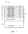
- Figure 1 shows a sequence of III-V layers 106-122 which are grown sequentially on a Ge substrate 102 in one embodiment of the present invention to form a multijunction solar cell 100.
- the Ge substrate 102 may further include a photoactive junction.
- the layers are epitaxially grown, meaning that they replicate the single crystalline structure of material.
- the growth parameters (deposition temperature, growth rate, compound alloy composition, and impurity dopant concentrations) are preferably optimized to provide layers with the desired electrical qualities and thickness, to thereby obtain the required overall cell performance.
- the epitaxial techniques which may be used to grow the cell layers include, by way of example, MOCVD (metal-organic chemical vapor deposition) epitaxy, sometimes called OMVPE (organic-metallic vapor phase epitaxy), MBE (molecular beam expitaxy), and MOMBE (metal- organic molecular beam epitaxy).
- MOCVD metal-organic chemical vapor deposition
- OMVPE organic-metallic vapor phase epitaxy
- MBE molecular beam expitaxy
- MOMBE metal- organic molecular beam epitaxy
- an N doped GaAs base layer 106 is grown over and overlays at least a portion of the substrate 102. At the interface between layer 102 and layer 106 a photoactive junction is formed.
- the photoactive junction is an N+GaAs/N+Ge heterodiode.
- a P-type Ge substrate 102 is used, and diffusion of As from the layer 106 forms an N/P junction in the substrate 102.
- a highly P doped GaAs emitter layer 108 is grown over at least a portion of the GaAs base layer 106.
- the base layer 106 and the emitter layer 108 together form a lower cell stage.
- a highly P doped AlGaAs window layer 110 overlays the emitter layer 108.
- a tunnel diode, including very highly doped P and N layers 112, 114 is grown over the window layer 110.
- the last two layers grown for the solar cell are respectively a highly P doped AlGaAs window 120, which is a thin, transparent layer that passivates (reduces carrier recombination) the surface of the emitter layer 118 of the top cell (GainP 2 ), and a GaAs cap-layer 122 onto which the front surface ohmic contacts are deposited.
- the contacts are in grid-finger form, to balance low electrical resistance and high optical transparency. However, other contact patterns may be used as well.
- the integral bypass diode is included in the monolithically-grown cell structure by the growth of several additional layers.
- the cap layer 122 is selectively removed between the gridlines, and anti-refiective coatings are deposited over the top window layer 120.
- the three cell, three-junction, solar cell 100, illustrated in Figure 1 is only one of many possible cell embodiments which can be used with the present invention.
- a complementary structure with the polarities of one or more layers switched (i. e. N doped layers are, instead, P doped, and P doped layers are, instead, N doped), may be used.
- the cell and diode configurations illustrated in the figures and discussed below can be changed from P/N to N/P.
- the doping concentrations or layer thicknesses may be varied.
- the solar cell 100 may include four or more photovoltaic cells, or only one or two cells.
- the solar cell may alternatively include only one junction or two or more junctions.
- the cell 100 may include four junctions.
- the solar cell 100 may include cells made from other materials, such as AlGaAs or InP.
- the substrate 102 may be formed using a variety of different materials.
- the solar cell 100 may use other semiconductors, such as GaAs, Si, or InP for the substrate, rather than the Ge substrate 102 illustrated in Figure 1 .
- insulating substrates such as sapphire, may be used.
- the substrate 102 is a single crystal. If the solar cell 100 is intended for space use, such as on a space vehicle or satellite, then the cell materials are preferably space-qualified for the appropriate space environment. For example, the solar cell 100 and bypass diode may be space qualified to operate in an AMO radiation environment.
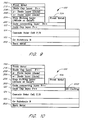
- bypass diode 212 is included in the solar cell structure using additional five grown layers 202, 204, 206, 208, 210.
- the layers 106-122 comprising the photovoltaic portions of the multijunction solar cell 100, are first grown, and the growth cycle is continued to grow the additional layers 202-210.
- the additional layers in order are:
- embodiments of the present invention may utilize a different number of layers, formed from different types of materials, and having different dopants than the embodiment described above.
- the use of the complementary structure that is, N/P rather than P/N, can similarly consist of N/P multijunction solar cells, and an N/P bypass diode.
- the diode 212 may be formed using lower bandgap materials, such as germanium or InGaAs.
- the layer 202 may be omitted, leaving the layer 204 to provide stop-etching and electrical conduction.
- the photoactive solar cell layers and the diode layers illustrated in Figure 2 are epitaxially grown using conventional MOCVD and/or MBE technologies.
- the front surface of the grown layer sequence is protected with a photoresist layer 302, which is exposed through a photomask (not shown) patterned to leave the diode layers covered with resist.
- the diode cap layer 210 and the N and P diode layers 206, 208 are etched down to the stop-etch layer 204. The etching may be performed using citric acid heated to 45°C.
- the stop etch layer 204 is removed where the photoresist layer 302 does not mask, and appropriate portions of the N doped GaAs connecting layer 202 is exposed.
- the etchant may be BHF (buffered hydrofloric) acid.
- the stop etch layer 204 is GalnP, then in another embodiment, the etchant may be HCL.
- the photoresist layer 302 is removed using acetone. Microstripping techniques may be used to remove any residual photoresist left remaining after the acetone removal process.
- the front contact fabrication process including corresponding photoresist coating, baking, exposing, developing, metal evaporation, and lift off operations, can take place.
- Another photoresist layer (not shown) is coated over the whole surface.
- the photoresist layer is then baked and exposed with a photomask which leaves opened areas where contacts are to be deposited to the front surface gridlines and pads, to a small region of the exposed N doped GaAs layer 202, and to the diode cap layer 210.
- Metals predominantly including Ag, are evaporated into the exposed areas and over the remaining photoresist layer.
- the photoresist In addition to the two contact areas 702, 704 illustrated in Figure 7 , the photoresist also provides open slots in the photoresist, to provide gridlines, and bars/pad contacts to the cell. Next, a lift-off process is performed. The solar cell slice 100 is immersed in acetone, causing the photoresist to swell, and thereby breaks the metal film everywhere except on the regions designated to retain contacts, including contacts 702, 704.
- metals are evaporated over the back surface of the Ge substrate 102 to form a back metal contact 802.
- the contacts 702, 704, 802 are then heat-treated or sintered.
- the GaAs cap layer 122 is etched off the major part of the exposed front surface, as illustrated in Figure 9 .
- the cap layer 122 remains under the metallized areas, forming part of a low resistance contact mechanism.
- the diode pad metal contacts 702, 704, and the small contacts shown around the diode 212 are protected with a resist mask, and on the rest of the surface, an anti-reflecting layer 1002 is deposited.
- the top, P-side, diode contact 702 is connected to the back cell (N-grid) contact 802 by bonding a thin interconnect 1102.
- the electrical connection between the P-layer 208 of the P/N GaAs diode 212 and the backside of the N doped Ge substrate 102 is formed by a C clamp 1102, which is bonded to both the front diode contact 702 and the rear Ge contact 802.
- the bypass diode 212 is connected across both of the photovoltaic cells.
- the bypass diode may be used to bypass one or more photovoltaic cells.
- one embodiment of the present invention can be used to bypass all the cells in a solar cell structure 100, or less than all the cells in the solar cell structure 100.
- a short contact between the diode top contact and a metallized area on a small trough etched down through the cascade cell layers 1206-1218 to expose the Ge substrate 1204 may be used, rather than a C-clamp.
- the trough may remove less than 1 % of the active cell area, and may be located close to the top contact of the bypass diode.
- the embodiment illustrated in Figure 12 includes a front metal contact 1224, a rear metal contact 1202, and an anti-reflective coasting 1226.
- Several different contact configurations may be used. By way of example:
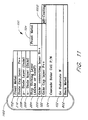
- Figure 13A illustrates a perspective view of one embodiment of the solar cell 100, including the bypass diode circuit 212.
- the front surface of the solar cell 100 includes grid lines 1302 interconnected by an ohmic bar 1306.
- the bar 1306 is shaped to provide an area or recess where the diode 212 is formed.
- the diode 212 is interconnected to the back contact 802 of the solar cell 100 using the C-clamp connector 1102 illustrated in Figure 11 .
- Figure 13B illustrates in greater detail the bypass diode 212 illustrated in Figure 13A .
- the sides of the diode 212 are interdigitated with the ohmic bar 1306. Thus, the distance between the diode 212 and the bar 1306 is reduced, and more of the bar 1306 is in proximity with the diode 212.
- three tabs 1304 are mounted on the solar cell 100 for interconnection to an adjoining assembly.
- the tabs 1304 may include a U-shaped stress relief section, also called a Z-tab.
- a first side of each of the tabs 1304 is connected to an anode of the cell 100.
- the solar cell 100 may be interconnected to a second solar cell by connecting a second side of the tabs 1304 to a cathode of the second solar cell.
- the tabs are formed from silver, silver-Invar, or silver-clad moly materials.
- a coverglass may be used to protect the solar cell/bypass diode device.
- the coverglass may be composed of ceria-doped borosilicate coverglass.
- the coverglass may have a thickness around 50 ⁇ m to 200 ⁇ m.
- the ceria-doped coverglass provides radiation resistant shielding for charged and uncharged particles.
- the coverglass will remain substantially transparent when exposed to an AMO space radiation environment spectrum (the spectrum found at Earth's orbit around the sun, outside of Earth's atmosphere).
- a major advantage of one embodiment of the integral bypass diode is that the diode does not extend above the front surface of the solar cell 100, and therefore does not require the use of a notched or slotted coverglass to accommodate the integral diode.
- the integral diode may extend above the front or top surface of the solar cell 100.
- coverglass materials and dimensions can be used as well.
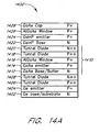
- FIG 14A illustrates still another embodiment of the present invention.
- the illustrated solar cell 1400 includes a novel buried protective bypass diode 1410.
- the protective bypass diode 1410 is used to protect the solar cell from reverse bias conditions which can result from the shadowing of the cell.
- the exemplary grown layer sequence illustrated in Figure 14A is similar to that of Figure 1A .
- Two additional buried layers 1406, 1408 are provided for polarity matching with the Ge+ emitter 1404.
- the solar cell 1400 includes a Ge substrate 1402 over which the Ge emitter layer 1404 is grown.
- Isolated diode layers 1412-1420 form a portion of the bypass diode function.
- Layers 1422, 1424 form the conventional top cell, over which is a window layer 1426, and a cap layer 1428.
- a complementary structure with the polarities of one or more layers switched from those illustrated in Figure 14A (i. e. P doped layers are, instead, N doped, and N doped layers are, instead, P doped), may be used.
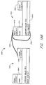
- the solar cell is processed, and, as illustrated in Figure 14B , a back metal contact 1430 and a front metal diode contact 1440 are formed. In addition, an anti-reflective coating 1432 is applied.
- a short integral connector 1436 is formed over an insulator 1434 from the cap layer 1428 on a small trough 1438 etched down through the cell layers 1420-1412 to the tunnel diode layer 1408.
- An interconnect such as a C-clamp 1442, may then be used to connect the front metal contact 1440 and the back metal contact 1430.
- the bypass diode 1410 is connected in an anti-parallel configuration with respect to the photovoltaic portions of the solar cell 1400 and thereby is configured to provide reverse bias protection to the photovoltaic portions of the solar cell 1400.
- a solar cell incorporating an integral diode onto cascaded cells has achieved efficiencies of well over 21%, and even over 23.5%. These efficiencies are comparable to conventional cascade cells lacking the integral bypass diode.
- the integral bypass diode has a forward bias voltage drop of approximately 1.4 to 1.8 volts when conducting 400 mA of forward current.
- the reverse breakdown voltage is sufficient to block current passing into the bypass diode when the solar cell is forward biased during normal, unshadowed, illumination. In one embodiment, the reverse breakdown voltage is greater than 2.5V.
- samples of one embodiment of the present invention have sustained repeated 10-second pulses of 400 mA of reverse current with no significant change in performance.
- the following performance changes were observed: Parameter Pre-test Measurement Post-test Measurement VOC (OPEN CIRCUIT VOLTAGE) 2476 mV 2476 mV ISC (SHORT CIRCUIT CURRENT) 360.5 mA 359.0 mA CFF (CURVE FIELD FACTOR) 81.5% 81.5% Efficiency 22.1 % 22 %
- the solar cell design described above is modified to even further facilitate its use in either space-based or terrestrial-based concentrator systems.
- non-concentrator systems there is a need to protect against shadowing of the solar cells from clouds, birds, buildings, antennas, or other structures.
- protective diodes are still used to protect solar cells from reverse bias conditions resulting from shadowing.
- solar cells in concentrator assemblies typically generate much more power than non-concentrator solar cells.
- the protective diodes need to be capable of dissipating heat associated with the much greater power that is bypassed.
- distributing multiple separated bypass integral diodes across at least a portion of the surface of the solar cell helps distribute the heat dissipation.
- each of the multiple integral diodes bypasses a portion of the reverse bias power, and correspondingly dissipates a portion of the associated heat.
- a single integral diode does not have to bypass all the reverse bias power or dissipate all the heat associated with such bypass function.
- the multiple integral bypass diodes may be formed using the same technique described above with regard to forming one integral diode. In one embodiment, different photomasks are used to form the diodes and diode contacts.
- FIG. 15A illustrates one method of interconnecting in series solar cells having integral bypass diodes.
- two solar cells 1502, 1510, with corresponding integral bypass diodes 1504, 1514 are interconnected to form a solar cell string 1500.
- a first interconnect 1508 is connected to a front contact 1506, overlaying cascaded cells of the solar cell 1502, and to a front contact 1512, overlaying the integral bypass diode 1514 of the solar cell 1510, thereby electrically coupling the solar cells 1502, 1510.
- the first interconnect 1508 may be a jumper bar, wire, or the like.
- a second interconnect 1518 is connected to the front contact 1506 of the solar cell 1502, and to a back contact 1516 of the solar cell 1510.
- the second interconnect 1518 may be a z-tab, wire, or the like.
- the bypass diodes 1504, 1514 are conveniently located on the edge or side opposite the Ohmic cell contact pads 1506, 1520.
- Figure 15B illustrates another method of interconnecting in series solar cells having integral bypass diodes.
- the first interconnect 1508 is connected to the front contact 1506 of the solar cell 1502, and to the front contact 1512 of the solar cell 1510.
- the second interconnect 1518 is connected to the front contact 1512 and to the back contact 1516 of the solar cell 1510.
- the second interconnect 1518 may be a C-clamp, wire, or the like.
- This embodiment can advantageously use only one interconnect between two adjacent cells, and the series connection between the cells can be made on the front surfaces of the cells.
- the cells can first have their corresponding C-clamps individually affixed by the cell manufacturer.
- the solar cell panel assembler can then appropriately position the cells in long strings, and then interconnect the front contacts of the cells as illustrated in Figure 15B . This procedure can provide for the efficient, high yield manufacture of solar cells, solar cell strings, and solar cell panels.
Landscapes
- Photovoltaic Devices (AREA)
Applications Claiming Priority (2)
| Application Number | Priority Date | Filing Date | Title |
|---|---|---|---|
| US8720698P | 1998-05-28 | 1998-05-28 | |
| EP99925702A EP1008188B1 (fr) | 1998-05-28 | 1999-05-19 | Cellule solaire comportant une diode intégrale en parallèle a croissance monolithique |
Related Parent Applications (2)
| Application Number | Title | Priority Date | Filing Date |
|---|---|---|---|
| EP99925702.5 Division | 1999-05-19 | ||
| EP99925702A Division EP1008188B1 (fr) | 1998-05-28 | 1999-05-19 | Cellule solaire comportant une diode intégrale en parallèle a croissance monolithique |
Publications (2)
| Publication Number | Publication Date |
|---|---|
| EP2197042A2 true EP2197042A2 (fr) | 2010-06-16 |
| EP2197042A3 EP2197042A3 (fr) | 2014-02-26 |
Family
ID=22203731
Family Applications (1)
| Application Number | Title | Priority Date | Filing Date |
|---|---|---|---|
| EP09014641.6A Withdrawn EP2197042A3 (fr) | 1998-05-28 | 1999-05-19 | Cellule solaire dotée d'une diode de dérivation à croissance monolithe intégrale |
Country Status (5)
| Country | Link |
|---|---|
| EP (1) | EP2197042A3 (fr) |
| JP (1) | JP4606959B2 (fr) |
| AT (1) | ATE411619T1 (fr) |
| DE (1) | DE69939754D1 (fr) |
| ES (2) | ES2312872T3 (fr) |
Cited By (2)
| Publication number | Priority date | Publication date | Assignee | Title |
|---|---|---|---|---|
| CN109920873A (zh) * | 2019-04-11 | 2019-06-21 | 青海黄河上游水电开发有限责任公司光伏产业技术分公司 | 一种全旁路保护晶体硅太阳电池组件 |
| CN110140219A (zh) * | 2016-09-26 | 2019-08-16 | 赫里亚泰克有限责任公司 | 在部分遮阴下具有改进的效率和使用寿命的用于将光转换成电能的有机构造元件 |
Families Citing this family (2)
| Publication number | Priority date | Publication date | Assignee | Title |
|---|---|---|---|---|
| DE102008006987A1 (de) * | 2008-01-31 | 2009-08-06 | Osram Opto Semiconductors Gmbh | Strahlungsempfänger und Verfahren zur Herstellung eines Strahlungsempfängers |
| JP2012516578A (ja) * | 2009-01-28 | 2012-07-19 | マイクロリンク デバイセズ, インク. | 酸化窓層を備えた高効率のiii−v族化合物半導体の太陽電池装置 |
Family Cites Families (9)
| Publication number | Priority date | Publication date | Assignee | Title |
|---|---|---|---|---|
| GB1382072A (en) * | 1972-02-03 | 1975-01-29 | Ferranti Ltd | Solar cells |
| JPS57204180A (en) * | 1981-06-09 | 1982-12-14 | Mitsubishi Electric Corp | Gaas solar battery element |
| JPS60240171A (ja) * | 1984-05-15 | 1985-11-29 | Mitsubishi Electric Corp | 太陽光発電装置 |
| MY104396A (en) * | 1988-02-05 | 1994-03-31 | Minnesota Mining & Mfg | Method for manufacturing an amorphous silicon thin film solar cell and schottky barrier diode on a common substrate. |
| DE68923061T2 (de) * | 1988-11-16 | 1995-11-09 | Mitsubishi Electric Corp | Sonnenzelle. |
| JPH0377382A (ja) * | 1989-08-19 | 1991-04-02 | Mitsubishi Electric Corp | 太陽電池セル |
| JPH0548134A (ja) * | 1991-08-07 | 1993-02-26 | Mitsubishi Electric Corp | 太陽電池とその製造方法 |
| JPH0964397A (ja) * | 1995-08-29 | 1997-03-07 | Canon Inc | 太陽電池および太陽電池モジュール |
| DE69941667D1 (de) * | 1998-05-28 | 2010-01-07 | Emcore Solar Power Inc | Solarzelle mit einer integrierten monolitisch gewachsenen Bypassdiode |
-
1999
- 1999-05-19 ES ES04005841T patent/ES2312872T3/es not_active Expired - Lifetime
- 1999-05-19 ES ES99925702T patent/ES2334526T3/es not_active Expired - Lifetime
- 1999-05-19 AT AT04005841T patent/ATE411619T1/de not_active IP Right Cessation
- 1999-05-19 DE DE69939754T patent/DE69939754D1/de not_active Expired - Lifetime
- 1999-05-19 EP EP09014641.6A patent/EP2197042A3/fr not_active Withdrawn
-
2005
- 2005-07-27 JP JP2005217577A patent/JP4606959B2/ja not_active Expired - Lifetime
Non-Patent Citations (1)
| Title |
|---|
| None |
Cited By (4)
| Publication number | Priority date | Publication date | Assignee | Title |
|---|---|---|---|---|
| CN110140219A (zh) * | 2016-09-26 | 2019-08-16 | 赫里亚泰克有限责任公司 | 在部分遮阴下具有改进的效率和使用寿命的用于将光转换成电能的有机构造元件 |
| CN110140219B (zh) * | 2016-09-26 | 2023-11-10 | 赫里亚泰克有限责任公司 | 在部分遮阴下具有改进的效率和使用寿命的用于将光转换成电能的有机构造元件 |
| CN109920873A (zh) * | 2019-04-11 | 2019-06-21 | 青海黄河上游水电开发有限责任公司光伏产业技术分公司 | 一种全旁路保护晶体硅太阳电池组件 |
| CN109920873B (zh) * | 2019-04-11 | 2024-04-05 | 青海黄河上游水电开发有限责任公司光伏产业技术分公司 | 一种全旁路保护晶体硅太阳电池组件 |
Also Published As
| Publication number | Publication date |
|---|---|
| ATE411619T1 (de) | 2008-10-15 |
| ES2312872T3 (es) | 2009-03-01 |
| JP2006013531A (ja) | 2006-01-12 |
| DE69939754D1 (de) | 2008-11-27 |
| ES2334526T3 (es) | 2010-03-11 |
| JP4606959B2 (ja) | 2011-01-05 |
| EP2197042A3 (fr) | 2014-02-26 |
Similar Documents
| Publication | Publication Date | Title |
|---|---|---|
| US6359210B2 (en) | Solar cell having an integral monolithically grown bypass diode | |
| EP1443566B1 (fr) | Cellule solaire comportant une diode de protection en parallele integrée monolithiquement | |
| US6617508B2 (en) | Solar cell having a front-mounted bypass diode | |
| WO1999062125A1 (fr) | Cellule solaire comportant une diode integrale en parallele a croissance monolithique | |
| US7732705B2 (en) | Reliable interconnection of solar cells including integral bypass diode | |
| US7687707B2 (en) | Via structures in solar cells with bypass diode | |
| JP3661941B2 (ja) | モノリシックバイパスダイオードおよび太陽電池ストリング装置 | |
| US5853497A (en) | High efficiency multi-junction solar cells | |
| US8263853B2 (en) | Wafer level interconnection of inverted metamorphic multijunction solar cells | |
| US5716459A (en) | Monolithically integrated solar cell microarray and fabrication method | |
| US4997491A (en) | Solar cell and a production method therefor | |
| EP1428267B1 (fr) | Cellule solaire comportant une diode en parallele de protection contre les polarisations inverses | |
| EP2197042A2 (fr) | Cellule solaire dotée d'une diode de dérivation à croissance monolithe intégrale | |
| JP2005512306A (ja) | 逆バイアス保護用バイパスダイオードを有する太陽電池装置及びその製造方法 |
Legal Events
| Date | Code | Title | Description |
|---|---|---|---|
| PUAI | Public reference made under article 153(3) epc to a published international application that has entered the european phase |
Free format text: ORIGINAL CODE: 0009012 |
|
| AC | Divisional application: reference to earlier application |
Ref document number: 1008188 Country of ref document: EP Kind code of ref document: P |
|
| AK | Designated contracting states |
Kind code of ref document: A2 Designated state(s): AT BE CH CY DE DK ES FI FR GB GR IE IT LI LU MC NL PT SE |
|
| PUAL | Search report despatched |
Free format text: ORIGINAL CODE: 0009013 |
|
| AK | Designated contracting states |
Kind code of ref document: A3 Designated state(s): AT BE CH CY DE DK ES FI FR GB GR IE IT LI LU MC NL PT SE |
|
| RIC1 | Information provided on ipc code assigned before grant |
Ipc: H01L 31/068 20120101AFI20140121BHEP Ipc: H01L 27/142 20140101ALI20140121BHEP |
|
| 17P | Request for examination filed |
Effective date: 20140826 |
|
| RAP1 | Party data changed (applicant data changed or rights of an application transferred) |
Owner name: SOLAERO TECHNOLOGIES CORP. |
|
| STAA | Information on the status of an ep patent application or granted ep patent |
Free format text: STATUS: EXAMINATION IS IN PROGRESS |
|
| 17Q | First examination report despatched |
Effective date: 20170328 |
|
| STAA | Information on the status of an ep patent application or granted ep patent |
Free format text: STATUS: THE APPLICATION HAS BEEN WITHDRAWN |
|
| 18W | Application withdrawn |
Effective date: 20181120 |