EP2200100A1 - Élément semi-conducteur au nitrure iii émettant de la lumière - Google Patents
Élément semi-conducteur au nitrure iii émettant de la lumière Download PDFInfo
- Publication number
- EP2200100A1 EP2200100A1 EP08834447A EP08834447A EP2200100A1 EP 2200100 A1 EP2200100 A1 EP 2200100A1 EP 08834447 A EP08834447 A EP 08834447A EP 08834447 A EP08834447 A EP 08834447A EP 2200100 A1 EP2200100 A1 EP 2200100A1
- Authority
- EP
- European Patent Office
- Prior art keywords
- light
- layer
- well
- emitting
- nitride semiconductor
- Prior art date
- Legal status (The legal status is an assumption and is not a legal conclusion. Google has not performed a legal analysis and makes no representation as to the accuracy of the status listed.)
- Withdrawn
Links
- 239000004065 semiconductor Substances 0.000 title claims abstract description 47
- 150000004767 nitrides Chemical class 0.000 title claims abstract description 42
- 239000000758 substrate Substances 0.000 claims abstract description 42
- 230000004888 barrier function Effects 0.000 claims abstract description 40
- 239000012535 impurity Substances 0.000 claims abstract description 28
- 239000000463 material Substances 0.000 claims abstract description 17
- 229910052733 gallium Inorganic materials 0.000 claims abstract description 9
- GYHNNYVSQQEPJS-UHFFFAOYSA-N Gallium Chemical compound [Ga] GYHNNYVSQQEPJS-UHFFFAOYSA-N 0.000 claims abstract description 8
- 239000011777 magnesium Substances 0.000 claims description 34
- 239000013078 crystal Substances 0.000 claims description 24
- 229910052710 silicon Inorganic materials 0.000 claims description 8
- 239000010703 silicon Substances 0.000 claims description 7
- XUIMIQQOPSSXEZ-UHFFFAOYSA-N Silicon Chemical compound [Si] XUIMIQQOPSSXEZ-UHFFFAOYSA-N 0.000 claims description 6
- 229910052749 magnesium Inorganic materials 0.000 claims description 5
- FYYHWMGAXLPEAU-UHFFFAOYSA-N Magnesium Chemical compound [Mg] FYYHWMGAXLPEAU-UHFFFAOYSA-N 0.000 claims description 4
- 238000009877 rendering Methods 0.000 abstract description 16
- 239000000203 mixture Substances 0.000 abstract description 12
- OAICVXFJPJFONN-UHFFFAOYSA-N Phosphorus Chemical compound [P] OAICVXFJPJFONN-UHFFFAOYSA-N 0.000 abstract description 11
- 239000010410 layer Substances 0.000 description 343
- IJGRMHOSHXDMSA-UHFFFAOYSA-N Atomic nitrogen Chemical compound N#N IJGRMHOSHXDMSA-UHFFFAOYSA-N 0.000 description 31
- 238000000034 method Methods 0.000 description 27
- 229910002601 GaN Inorganic materials 0.000 description 26
- JMASRVWKEDWRBT-UHFFFAOYSA-N Gallium nitride Chemical compound [Ga]#N JMASRVWKEDWRBT-UHFFFAOYSA-N 0.000 description 25
- 238000001451 molecular beam epitaxy Methods 0.000 description 23
- 125000004429 atom Chemical group 0.000 description 15
- 230000000295 complement effect Effects 0.000 description 15
- 229910052757 nitrogen Inorganic materials 0.000 description 15
- 230000015572 biosynthetic process Effects 0.000 description 13
- 239000003086 colorant Substances 0.000 description 11
- 238000000103 photoluminescence spectrum Methods 0.000 description 9
- 230000000007 visual effect Effects 0.000 description 7
- 238000009434 installation Methods 0.000 description 5
- 238000002488 metal-organic chemical vapour deposition Methods 0.000 description 5
- 239000002344 surface layer Substances 0.000 description 5
- PMHQVHHXPFUNSP-UHFFFAOYSA-M copper(1+);methylsulfanylmethane;bromide Chemical compound Br[Cu].CSC PMHQVHHXPFUNSP-UHFFFAOYSA-M 0.000 description 4
- 238000000295 emission spectrum Methods 0.000 description 4
- 230000005284 excitation Effects 0.000 description 4
- 230000004913 activation Effects 0.000 description 3
- 238000001312 dry etching Methods 0.000 description 3
- 239000001257 hydrogen Substances 0.000 description 3
- 229910052739 hydrogen Inorganic materials 0.000 description 3
- BASFCYQUMIYNBI-UHFFFAOYSA-N platinum Chemical compound [Pt] BASFCYQUMIYNBI-UHFFFAOYSA-N 0.000 description 3
- 230000006798 recombination Effects 0.000 description 3
- 238000005215 recombination Methods 0.000 description 3
- 229910019901 yttrium aluminum garnet Inorganic materials 0.000 description 3
- UFHFLCQGNIYNRP-UHFFFAOYSA-N Hydrogen Chemical compound [H][H] UFHFLCQGNIYNRP-UHFFFAOYSA-N 0.000 description 2
- RNQKDQAVIXDKAG-UHFFFAOYSA-N aluminum gallium Chemical compound [Al].[Ga] RNQKDQAVIXDKAG-UHFFFAOYSA-N 0.000 description 2
- NWAIGJYBQQYSPW-UHFFFAOYSA-N azanylidyneindigane Chemical compound [In]#N NWAIGJYBQQYSPW-UHFFFAOYSA-N 0.000 description 2
- UIZLQMLDSWKZGC-UHFFFAOYSA-N cadmium helium Chemical compound [He].[Cd] UIZLQMLDSWKZGC-UHFFFAOYSA-N 0.000 description 2
- 239000000969 carrier Substances 0.000 description 2
- 229910052738 indium Inorganic materials 0.000 description 2
- 229910052751 metal Inorganic materials 0.000 description 2
- 239000002184 metal Substances 0.000 description 2
- 239000002994 raw material Substances 0.000 description 2
- 229910052594 sapphire Inorganic materials 0.000 description 2
- 238000001228 spectrum Methods 0.000 description 2
- 238000000927 vapour-phase epitaxy Methods 0.000 description 2
- PIGFYZPCRLYGLF-UHFFFAOYSA-N Aluminum nitride Chemical compound [Al]#N PIGFYZPCRLYGLF-UHFFFAOYSA-N 0.000 description 1
- XLOMVQKBTHCTTD-UHFFFAOYSA-N Zinc monoxide Chemical compound [Zn]=O XLOMVQKBTHCTTD-UHFFFAOYSA-N 0.000 description 1
- 229910052782 aluminium Inorganic materials 0.000 description 1
- XAGFODPZIPBFFR-UHFFFAOYSA-N aluminium Chemical compound [Al] XAGFODPZIPBFFR-UHFFFAOYSA-N 0.000 description 1
- JNDMLEXHDPKVFC-UHFFFAOYSA-N aluminum;oxygen(2-);yttrium(3+) Chemical compound [O-2].[O-2].[O-2].[Al+3].[Y+3] JNDMLEXHDPKVFC-UHFFFAOYSA-N 0.000 description 1
- 238000005229 chemical vapour deposition Methods 0.000 description 1
- 238000011109 contamination Methods 0.000 description 1
- 238000006356 dehydrogenation reaction Methods 0.000 description 1
- 230000006866 deterioration Effects 0.000 description 1
- 238000010586 diagram Methods 0.000 description 1
- 238000009792 diffusion process Methods 0.000 description 1
- 230000001747 exhibiting effect Effects 0.000 description 1
- 150000004678 hydrides Chemical class 0.000 description 1
- 150000002431 hydrogen Chemical class 0.000 description 1
- APFVFJFRJDLVQX-UHFFFAOYSA-N indium atom Chemical compound [In] APFVFJFRJDLVQX-UHFFFAOYSA-N 0.000 description 1
- 230000010354 integration Effects 0.000 description 1
- 238000004519 manufacturing process Methods 0.000 description 1
- 150000007522 mineralic acids Chemical class 0.000 description 1
- 229910052697 platinum Inorganic materials 0.000 description 1
- 230000005855 radiation Effects 0.000 description 1
- 229910052761 rare earth metal Inorganic materials 0.000 description 1
- 239000011347 resin Substances 0.000 description 1
- 229920005989 resin Polymers 0.000 description 1
- 239000010980 sapphire Substances 0.000 description 1
- 238000001004 secondary ion mass spectrometry Methods 0.000 description 1
- HBMJWWWQQXIZIP-UHFFFAOYSA-N silicon carbide Chemical compound [Si+]#[C-] HBMJWWWQQXIZIP-UHFFFAOYSA-N 0.000 description 1
- JBQYATWDVHIOAR-UHFFFAOYSA-N tellanylidenegermanium Chemical compound [Te]=[Ge] JBQYATWDVHIOAR-UHFFFAOYSA-N 0.000 description 1
- 230000007704 transition Effects 0.000 description 1
- 239000011701 zinc Substances 0.000 description 1
Images


Classifications
-
- H—ELECTRICITY
- H10—SEMICONDUCTOR DEVICES; ELECTRIC SOLID-STATE DEVICES NOT OTHERWISE PROVIDED FOR
- H10H—INORGANIC LIGHT-EMITTING SEMICONDUCTOR DEVICES HAVING POTENTIAL BARRIERS
- H10H20/00—Individual inorganic light-emitting semiconductor devices having potential barriers, e.g. light-emitting diodes [LED]
- H10H20/80—Constructional details
- H10H20/81—Bodies
- H10H20/811—Bodies having quantum effect structures or superlattices, e.g. tunnel junctions
- H10H20/812—Bodies having quantum effect structures or superlattices, e.g. tunnel junctions within the light-emitting regions, e.g. having quantum confinement structures
-
- H—ELECTRICITY
- H10—SEMICONDUCTOR DEVICES; ELECTRIC SOLID-STATE DEVICES NOT OTHERWISE PROVIDED FOR
- H10H—INORGANIC LIGHT-EMITTING SEMICONDUCTOR DEVICES HAVING POTENTIAL BARRIERS
- H10H20/00—Individual inorganic light-emitting semiconductor devices having potential barriers, e.g. light-emitting diodes [LED]
- H10H20/80—Constructional details
- H10H20/81—Bodies
- H10H20/813—Bodies having a plurality of light-emitting regions, e.g. multi-junction LEDs or light-emitting devices having photoluminescent regions within the bodies
-
- H—ELECTRICITY
- H10—SEMICONDUCTOR DEVICES; ELECTRIC SOLID-STATE DEVICES NOT OTHERWISE PROVIDED FOR
- H10H—INORGANIC LIGHT-EMITTING SEMICONDUCTOR DEVICES HAVING POTENTIAL BARRIERS
- H10H20/00—Individual inorganic light-emitting semiconductor devices having potential barriers, e.g. light-emitting diodes [LED]
- H10H20/80—Constructional details
- H10H20/81—Bodies
- H10H20/822—Materials of the light-emitting regions
- H10H20/824—Materials of the light-emitting regions comprising only Group III-V materials, e.g. GaP
- H10H20/825—Materials of the light-emitting regions comprising only Group III-V materials, e.g. GaP containing nitrogen, e.g. GaN
Definitions
- the present invention relates to a Group III nitride semiconductor light-emitting device comprising a substrate and a light-emitting layer having themultiple quantumwell structure that comprises barrier layers and well layers formed of a gallium-containing Group III nitride semiconductor material provided on the surface of the substrate.
- a Group III nitride semiconductor material such as gallium indium nitride (GaInN) has been conventionally used for a light-emitting layer of a short-wavelength light-emitting diode (abbr.: LED) of, for example, white or blue or a laser diode (abbr.: LD) (see, for example, JP-B No. 55-3834 ).
- LED short-wavelength light-emitting diode
- LD laser diode
- Aluminum gallium nitride (AlGaN) has been used as a material for a light-emitting layer of a near-ultraviolet LED or an ultraviolet LED (see, for example, JP-A No. 2001-60719 ).
- One type of the conventional white LEDs comprises chip or lamp shaped red, green, and blue LEDs respectively emitting color lights of red (R), green (G), and blue (B), which are light' s three primary colors.
- the numbers of red, green, and blue LEDs used respectively correspond to the relative emission intensity ratios.
- the LEDs are integrated and arranged on the same substrate, and, as a whole, the mixture of red, blue, and green provides emission of white light (see, for example, JP-A Nos. 6-314824 , 7-7223 , 7-15044 , 7-235624 , 7-288341 , 7-283438 , and 7-335942 ).
- This type of white LED may be referred to as an array-type (module) white LED.
- Another type of conventional white LED includes light-emitting layers which are separately provided on one substrate, each emit red, green, and blue lights, and are made of, for example, a Group III nitride semiconductor (see, for example, JP-A Nos. 6-53549 and 7-183576 ).
- the white LED may be referred to as an RGB-type white LED which emits white color by mixing lights corresponding to the light's three primary colors (red (R), green (G), and blue (B)) emitted from respective light-emitting layers.
- Still another type of conventional white LED is a white LED having light-emitting layers which respectively emit light in a relation of complementary colors and are provided on a single substrate.
- a Group III nitride semiconductor light-emitting layer emitting blue light and a light-emitting layer emitting yellow light are respectively provided on the same substrate, and two lights which are emitted from the respective light-emitting layers different in color (for example, blue and yellow) and wavelength are mixed to emit white color (see, for example, JP-A No. 2001-257379 ).
- the white LED may be referred to as a complementary color type white LED utilizing the fact that when two lights of different colors (different wavelengths) in a complementary relationship are mixed, the mixture is visually perceived as a white light.
- the LED which utilizes light emitted from a Group III nitride semiconductor light-emitting layer to excite a phosphor emitting fluorescence with a wavelength different from the light emitted from the light-emitting layer, and, thus, to convert the wavelength of the emitted light (see, for example, JP-A No. 7-99345 ).
- the LED may be referred to as a fluorescent-type white LED which utilizes blue light or ultraviolet light emitted from a Group III nitride semiconductor light-emitting layer to excite a phosphor, and, thus, to emit white light (see, for example, Japanese Patent Nos.
- yttrium aluminum garnet Y 3 Al 5 O 12
- Japanese Patent Nos. 2927279 , 3503139 and 3700502 Japanese Patent Nos. 2927279 , 3503139 and 3700502 .
- a plane area of the light-emitting layers respectively emitting red, green, or blue light is much smaller than the installation plane area required for integration and arrangement of the chip or lamp shaped red, green, or blue LEDs (see JP-A Nos. 6-314824 and 7-15044 to 7-335942 ).
- the plane area occupied by the light-emitting layers providing light emission is extremely smaller than the plane area required for installation of the lamps, it is disadvantageous in obtaining a light-emitting device with high luminous intensity (lumen/area).
- the outer diameter (the diameter) of the lamp is generally 3 to 5 mm (see paragraph (0007) of JP-A No. 6-314824 ).
- the plane area is 0.09 mm 2 , which is much smaller than the plane area of the lamp (about 20 mm 2 ).
- the light-emitting layers which can respectively emit red (R), green (B), and blue (B) light are required to be separately provided.
- a clad layer or the like accompanying the light-emitting layer are required to be provided for each of the light-emitting layers in order to confine carriers (electrons and electron holes) in the light-emitting layer and confine light emission caused by radiative recombination of the carriers.
- a plurality of light-emitting layers are required to be provided on a single substrate, and, more preferably, the light-emitting layers and the clad layers or the like hetero-junctionedwith the respective light-emitting layers are required to be provided.
- the process for forming the RGB-type white LED is complex and redundant.
- p-type and n-type electrodes are required to be provided for each light-emitting layer emitting different color light. Since the electrodes need to be provided in the clad layer of the conductivity type corresponding to each of the electrodes and the like, the light-emitting layer is scraped and removed, leading to deterioration of the luminous intensity of each emission.
- the complementary color type white LED two or more light-emitting layers are required to be provided in order to emit lights of colors in a complementary relationship.
- clad layers of the light-emitting layers are required to be joined to form a light-emitting part having a single hetero- (abbr. : SH) or double hetero- (abbr.: DH) junction structure.
- SH single hetero-
- DH double hetero-
- the total plane area of the light-emitting layer emitting blue or yellow light is smaller than the plane area required for arranging the LED, and therefore, it is not necessarily advantageous to obtain a light-emitting device with high luminous intensity.
- the complementary color type white LED there is a problem that the color tone of resulting white light is slightly changed, depending on the wavelength of light of two colors in a complementary relationship that are mixed with each other to obtain the white light.
- colors of at most two lights with different wavelengths are usually mixed, and therefore, in any case, it is technically difficult to stably obtain a white LED exhibiting high and stable color rendering properties.
- the wavelength of the light emitted from the light-emitting layer which acts as an excitation light, should be kept constant with good reproducibility, and thus it is technically difficult.
- the composition of, for example, Y 3 Al 5 O 12 used as a phosphor and containing a rare-earth element should be artificially and finely adjusted according to variation in the wavelength of emission from the light-emitting layers.
- the present invention has been proposed in view of the above circumstances and an object thereof is to provide a Group III nitride semiconductor light-emitting device which has a simple structure that can be easily formed, can enhance luminous intensity, can obtain high and stable color rendering properties, and does not need fine adjustment of a composition of a phosphor.
- the light-emitting layer has the multiple quantum well structure comprising the barrier layers and the well layers. According to this constitution, a white light-emitting device can be easily formed with a simple structure, and since the installation area is substantially the same as the plane area of the light-emitting layer, the luminous intensity can be enhanced.
- only one light-emitting layer is provided, by virtue of the use of the light-emitting layer having the multiple quantum well structure capable of providing multiwavelength emission, only the single light-emitting layer may be provided with p-type and n-type electrodes. As compared with the case of the conventional RGB-type white LED, a region of the light-emitting layer that should be scraped and removed can be significantly reduced, and the luminous efficiency can be improved.
- the well layer is constituted of a plurality of well layers having different thicknesses, the wavelengths of a plurality of emissions from the well layers providing multicolor emission can be superimposed, and high and stable color rendering properties of white light emission can be obtained. Since the white light can be obtained even without using a fluorescent material, the fine composition adjustment of a phosphor is not required.
- the acceptor impurities are intentionally added to each well layer, the well layer which independently provides multicolor emission with different wavelengths can be constituted, and the single light-emitting layer having the multiple quantum well structure, which can independently provide multicolor emission, can be provided. Therefore, the high and stable color rendering properties of white light emission can be obtained. Furthermore, since the white light can be obtained even without using a fluorescent material, the fine composition adjustment of a phosphor is not required.
- the well layer is constituted of a layer providing the same conductivity type as that of the barrier layer, the formation of p-n junction with the barrier layer can be prevented, and thus the light-emitting layer having the multiple quantum well structure with excellent conductivity can be constituted.
- the well layers each made of a Group III nitride semiconductor layer are arranged so that the thickness of the well layers is sequentially reduced from the surface side of the substrate toward the direction of taking out the light emission from the light-emitting layer, whereby the light-emitting layer having the multiple quantum well structure is constituted. Therefore, light emitted from each well layer constituting the multiple quantum well structure can be efficiently taken in a visual field direction.
- the well layers which have a large width and emit multiwavelength light having a low quantum level and including a long-wavelength emission component are arranged on the surface side of the substrate, and the well layers which have a small width and emit multiwavelength light having a high quantum level and including a shorter wavelength emission component are arranged in the light taking out direction, whereby the light-emitting layer having the multiple quantum well structure is constituted. Namely, none of short-wavelength emissions passes through the well layers emitting light with a longer wavelength.
- the light emitted from the well layers arranged on the surface side of the substrate is not absorbed in the well layers arranged in the light taking out direction, but can be taken out in the external visual field direction, and thus the light emitted from each well layer can be efficiently taken out in the visual field direction.
- a white LED with excellent color rendering properties and high intensity can be realized.
- the light-emitting layer having the multiple quantum well structure is constituted by using a plurality of well layers having different atomic concentrations of the acceptor impurities added thereto and providing a plurality of emissions with different wavelengths. Consequently, the single light-emitting layer independently providing multiwavelength emission can be obtained, and it is possible to provide a white LED with more excellent color rendering properties than, for example, the so-called complementary color type white LED which provides white light by mixing two lights which are in a relationship of complementary colors and have different wavelengths.
- FIG. 1 is a schematic view schematically showing a cross-sectional structure of a Group III nitride semiconductor light-emitting device of the present invention.
- the Group III nitride semiconductor light-emitting device of the present invention is a white light-emitting device comprising a substrate 1 and a light-emitting layer 5 having a multiple quantum well structure comprising barrier layers 5a and well layers 5b formed of a gallium-containing Group III nitride semiconductor material provided on the surface of the substrate 1.
- Each of the well layers 5b constituting the multiple quantum well structure is made of a Group III nitride semiconductor layer having the same conductivity type as that of the barrier layer 5a. Acceptor impurities are added to the well layers 5b, and the well layers 5b are formed to have thicknesses different from one another.
- the substrate 1 may include a substrate formed of an insulating or electroconductive crystalline oxide such as sapphire ( ⁇ -Al 2 O 3 single crystal) and zinc oxide (ZnO) with a polar or nonpolar crystal face as its surface, carbide crystal such as 6H, 4H, or 3C silicon carbide (SiC), and semiconductor crystal of silicon (Si).
- an insulating or electroconductive crystalline oxide such as sapphire ( ⁇ -Al 2 O 3 single crystal) and zinc oxide (ZnO) with a polar or nonpolar crystal face as its surface
- carbide crystal such as 6H, 4H, or 3C silicon carbide (SiC)
- semiconductor crystal of silicon Si
- silicon single crystal having an n-type or p-type conductivity and having a ⁇ 111 ⁇ crystal face as its surface can be suitably used as the substrate for use in formation of the multiple quantum well structure on its surface, according to the present invention.
- the well layer 5b constituting the multiple quantum well structure formed on the surface of the substrate 1 is made of a material which can independently and simultaneously emit light with a plurality of different wavelengths. Considering the color rendering properties of light emitted from LED, it is preferable that a large number of lights (withmultiple wavelengths) emitted from the well layer 5b are dispersed in a wide wavelength range. In order to obtain multiwavelength emissions over a wide wavelength range, it is preferable that in the multiple quantum well structure, the well layer 5b is formed of a semiconductor material with a large band gap energy.
- the semiconductor material with a large band gap energy may include a Group III nitride semiconductor material containing gallium (Ga).
- the well layer 5b can be preferably made of a wide band gap semiconductor material such as gallium nitride (GaN) and Ga x In 1-x N (0 ⁇ x ⁇ 1) that is amixedcrystalofgalliumnitride (GaN) andindiumnitride (InN).
- GaN gallium nitride
- Ga x In 1-x N (0 ⁇ x ⁇ 1)
- InN indiumnitride
- the barrier layer 5a constituting the multiple quantum well structure along with the well layer 5b ismade of, for example, a Group III nitride semiconductor material with a band gap energy larger than the well layer 5b.
- the barrier layer 5a is made of GaN.
- the barrier layer 5a and the well layer 5b constituting the multiple quantum well structure are made of layers having the same conductivity type.
- the n-type well layer 5b and the n-type barrier layer 5a constitute the n-type multiple quantum well structure as a whole. According to this constitution, the formation of p-n junction between the well layer 5b and the barrier layer 5a can be avoided, and thus the light-emitting layer 5 having the multiple quantum well structure with excellent conductivity can be constituted.
- impurities are not essentially added to the well layer 5b.
- the well layer can be utilized as the well layer 5b according to the present invention.
- the well layer 5b constituting the multiple quantum well structure is particularly made of a Group III nitride semiconductor layer containing Ga and acceptor impurities added thereto.
- the well layer 5b is made of n-type mixed crystal Ga 0.75 In 0.25 N containing the acceptor impurities added thereto.
- the well layer 5b having the same conductivity type as that of the barrier layer 5a and containing the acceptor impurities, by virtue of mixing of colors, can independently provide multiwavelength light composed of wavelengths that are different from each other and advantageous to obtain white light.
- a technique of forming the light-emitting layer 5 containing GaInN and zinc (Zn) added as the acceptor impurities is disclosed (see, JP-B No. 55-3834 ).
- the well layer 5b to which only Zn has been added as the acceptor impurities has a large resistance and fails to be stably formed so as to have a sufficient conductivity.
- magnesium (Mg) among Group II impurities that can be used as an acceptor for the Group III nitride semiconductor can be suitably used.
- the light-emitting layer 5 having the multiple quantum well structure according to the present invention can be formed by a vapor-phase epitaxy method, such as a metal organic chemical vapor deposition (abbreviated to, for example, MOCVD or MOVPE) method, a molecular beam epitaxy (MBE) method, a hydride method, andahalidemethod.
- a metal organic chemical vapor deposition abbreviated to, for example, MOCVD or MOVPE
- MBE molecular beam epitaxy
- the barrier layer 5a and the well layer 5b can be formed at a lower temperature as compared with the other vapor-phase epitaxy methods. Therefore, for example, the MBE method is growth means advantageous in terms of preventing Mg atoms which are used for the formation of the well layer 5b according to the present invention from thermally diffusing into the barrier layer 5a.
- the thickness of the well layer 5b containing Mg as the acceptor impurities is preferably not less than 1 nm and not more than 20 nm.
- An extremely thin well layer 5b having a thickness of less than 1 nm lacks two-dimensional continuity of layers (films) and therefore results in increase of an electrical resistance related to conduction of operating current to a light-emitting device, especially current diffusion in a horizontal (lateral) direction or results in decrease in a light-emitting region.
- the extremely thin well layer 5b is disadvantageous.
- even when the well layer 5b having a film thickness of more than 20 nm is used, many quantum levels different in energy level cannotbe satisfactorily formed.
- this well layer is also disadvantageous in that many emissions with different wavelengths based on transition between various quantum levels cannot be obtained.
- the Group III nitride semiconductor layer can typically be grown under a vacuum environment free from hydrogen. Therefore, the MBE method is advantageous in terms of easily forming, for example, a low resistance p-type Ga x In 1-x N (0 ⁇ X ⁇ 1) layer containing a large amount of electrically activated Mg (operated as an acceptor).
- a low resistance p-type Ga x In 1-x N 0. ⁇ X ⁇ 1
- Mg operate as an acceptor.
- N 2 nitrogen
- the electrical activation ratio of Mg (as a matter of convenience, it is represented by a value (%) obtained by dividing the carrier concentration by the concentration of Mg atoms) is 53% in an as-grown state.
- the MBE method like the Mg-doped GaN layer grown by MOCVD method, it is advantageous that the p-type Ga x In 1-x N (0 ⁇ X ⁇ 1) layer with the electrical activation ratio of not less than 50% can be easily formed without requiring a dehydrogenation treatment for the same layer.
- the multiple quantum well structure is constituted by a pair of structural units comprising a joint structure of one well layer 5b containing the acceptor impurities such as Mg and one barrier layer 5a having the same conductivity type as that of the well layer 5b
- the number of the pairs of structural units constituting the multiple quantum well structure is preferably not less than 3 pairs and not more than 40 pairs. Even when only one well layer 5b according to the present invention is provided, the well layer 5b can emit multiwavelength light; however, in order to obtain emission of light with more excellent color rendering properties, the number of the pairs of structural units is preferably not less than 4.
- FIG. 2 shows an example ofaphotoluminescence (abbr.
- the light-emitting layer 5 having the multiple quantum well structure which comprises 30 pairs of the well layer 5b made of Mg-doped n-type mixed crystal Ga 0.85 In 0.15 N grown by the MBE method and the GaN barrier layer 5a grown by the MBE method (one pair is an assembly of one barrier layer 5a and one well layer 5b).
- the thickness of the well layer 5b constituting the multiple quantum well structure is 4 nm, and the thickness of the barrier layer 5a is 10 nm.
- the horizontal axis represents emission wavelength (unit: ⁇ )
- the vertical axis represents emission intensity (unit: arbitrary unit).
- the light-emitting layer 5 having the multiple quantum well structure according to the present invention comprising the well layer 5b containing the acceptor impurities, emits three lights (represented by ⁇ 2 to ⁇ 4 in FIG. 2 ) with different wavelengths in a wavelength range of not less than 400 nm (4000 angstroms) and not more than 500 nm (5000 angstroms) .
- a total of six lights represented by ⁇ 1 to ⁇ 6 in FIG. 2
- a total of six lights can be emitted in a wavelength range of not less than the wavelength of the band-edge emission (in this example, 365 nm) and not more than 650 nm.
- a difference in wavelength between the adjacent lights is 17.5 nm between lights on the short wavelength side, for example, ⁇ 1 and ⁇ 2 ; however, it is characterized in that as the wavelength of light emission is longer, the difference in wavelength between emissions tends to become gradually larger, and the difference in wavelength between the lights ⁇ 5 and ⁇ 6 is 55.5 nm.
- the aspects of appearance of the emission peak of the multiwavelength light is different from the aspects of appearance of the so-called shoulder peak generated in a "shoulder part" of a major photoluminescence spectrum from the light-emitting layer 5 formed by the MOCVD method and doped with Si and Mg, as can also be clearly seen in the interval of the wavelength between emitted lights.
- the reason that the multiwavelength lights are emitted even when the well layers have a fixed thickness is attributed to the fact that various levels providing radiation recombination are formed due to addition of an acceptor.
- the well layer 5b which can independently and simultaneously emit the multiwavelength light
- the well layers 5b containing the acceptor impurities are arranged so that the thickness of the well layers 5b is reduced from the surface side of the substrate 1 toward the direction of taking out the light emission from the light-emitting layer 5, it is advantageous in obtaining a white LED excellent in an efficiency of taking light emission to the outside.
- the well layer 5b having a small thickness emits the multiwavelength light containing many short-wavelength emission components.
- the well layer 5b having a large thickness emits the multiwavelength light containing many emission components of long-wavelength light.
- the short-wavelength emission is absorbed in the well layer 5b leading to long-wavelength emission. Therefore, when the well layers 5b are arranged so that the thickness of the well layers 5b is reduced from the surface side of the substrate 1 toward the direction of taking out the light emission from the light-emitting layer 5, it is suitable for preventing the light emitted from the well layer 5b located on the surface side of the substrate 1 from being absorbed, and transmitting the light toward an external visual field direction.
- the white LED with excellent color rendering properties can be provided.
- the white LED with excellent color rendering properties can be constituted.
- a plurality of well layers 5b emitting light in a band having a low luminosity factor and having the same thickness are arranged, and further well layers 5b are arranged above the well layers 5b so that the thickness of the upper well layers 5b are sequentially reduced in the direction of taking out light emission, whereby the multiple quantum well structure of the light-emitting layer 5 may be constituted.
- each of the well layers 5b made of mixed crystal Ga x In 1-x N (0 ⁇ X ⁇ 1) can be formed so that the composition (1-X) of indium is varied.
- a growth method such as the MBE method and the MOCVD method
- a growth temperature of the well layers 5b and supply ratios of Ga and In raw materials are required to be changed to form the well layers 5b with the varied In compositions. Therefore, under the conditions of the same growth temperature and the raw material supply ratio, compared with the technique of simply adjusting the growth time to control the thickness of the well layer 5b, a troublesome operation should be performed.
- the wavelength of the light emitted from each of the well layers 5b varying in atomic concentration of the acceptor impurities varies according to the atomic concentration of the acceptor impurities.
- the atomic concentration of the acceptor impurities contained in the well layer 5b is changed, whereby it becomes more suitable for control of the wavelength range allowing the appearance of the multiwavelength light.
- the multiwavelength light can be allowed to appear in the wavelength range of not less than 400 nm and not more than 600 nm.
- the light-emitting layer 5 has the multiple quantum well structure comprising the barrier layers 5a and the well layer 5b, and therefore, the light-emitting layer providing multiple wavelength can be easily formed with a simple structure, and since the installation plane area is substantially the same as the plane area of the light-emitting layer 5, the luminous intensity can be enhanced. Further, since a single light-emitting layer 5 is provided, a p-type or n-type electrode may be provided so as to correspond only to the light-emitting layer 5, and as compared with the case of the RGB-type white LED and the complementary color type white LED, the area of the light-emitting layer 5 to be scraped can be significantly reduced, whereby a light-emission efficiency can be improved.
- the well layers 5b are constituted of a plurality of well layers 5b different in thickness, whereby each of the well layers 5b can emit multicolor lights with wavelengths different from one another, white light emission with high and stable color rendering properties can be obtained, and white light can be obtained without using a fluorescent material. Therefore, fine composition adjustment of a phosphor is not required.
- the acceptor impurities are intentionally added to each well layer 5b, and therefore, the light-emitting layer 5, which emits multicolor lights with different wavelengths while only one light-emitting layer 5 is provided, can be constituted.
- the multicolor emission property the high and stable color rendering properties of white light emission can be obtained, and white light can be obtained without using a fluorescent material. Therefore, fine composition adjustment of a phosphor is not required.
- the well layer 5b is made of a layer having the same conductivity type of that of the barrier layer 5a, the formation of p-n junction between the well layer 5b and the barrier layer 5a can be avoided, and thus the light-emitting layer 5 having the multiple quantumwell structure with excellent conductivity can be formed.
- the light-emitting layer 5 having the multiple quantum well structure is formed so that the well layers 5b each made of a Group III nitride semiconductor layer are arranged so that the thickness of each of the well layers 5b is sequentially reduced from the surface side of the substrate 1 toward the direction of taking out the light emission from the light-emitting layer 5, whereby the light emitted from each of the well layers 5b constituting the multiple quantum well structure can be efficiently taken in the visual field direction.
- the well layers 5b which have a large layer width and emit multiwavelength light having a low quantum level and including a long-wavelength emission component are arranged on the surface side of the substrate 1, and the well layers 5b which have a small layer width and emit multiwavelength light having a high quantum level and including a shorter wavelength emission component are arranged in the light taking out direction, whereby the light-emitting layer 5 having the multiple quantum well structure is formed. Under this structure, short-wavelength emission does not pass through the well layer 5b emitting longer wavelength light.
- the light emitted from the well layers 5b arranged on the surface side of the substrate is not absorbed in the well layers 5b arranged in the light taking out direction, the emitted light can be taken out in the external visual field direction, and the light emitted from each well layer 5b canbe efficientlytaken out in the visual fielddirection.
- a white LED with excellent color rendering properties and high intensity can be realized.
- the light-emitting layer 5 having the multiple quantum well structure is formed using a plurality of well layers 5b, which contain acceptor impurities with different atomic concentrations and provide a plurality of emissions with different wavelengths while only one light-emitting layer is provided. Therefore, the light-emitting layer 5 providing multiwavelength emission comprising superimposed lights emitted from respective well layers 5b is obtained, and it is possible to provide a white LED with more excellent color rendering properties than, for example, the so-called complementary color type white LED which provides white light by mixing two lights which are in a relation of complementary colors and have different wavelengths.
- FIG. 3 is a schematic cross-sectional view showing a structure of a Group III nitride semiconductor light-emitting device comprising a light-emitting layer having the multiple quantum well structure of a first embodiment.
- FIG. 4 shows a photoluminescence spectrum radiated from the light-emitting layer having the multiple quantum well structure.
- the horizontal axis represents emission wavelength (unit: ⁇ )
- the vertical axis represents emission intensity (unit: arbitrary unit).
- a ⁇ 111 ⁇ silicon single crystal (silicon) was used as a substrate 101.
- the surface of the substrate 101 was cleaned with an inorganic acid, and thereafter the substrate 101 was conveyed into a growth chamber of a molecular beam epitaxy (MBE) growth system.
- the growth chamber was then evacuated to ultra-high vacuum. Thereafter, the temperature of the substrate 101 was increased to 780°C while keeping the degree of vacuum in the growth chamber, and the substrate 101 was continuously heated until the surface 101a of the substrate 101 provides reconstitution of a (7 ⁇ 7) structure.
- MBE molecular beam epitaxy
- an MBE growth method nitrogen plasma MBE
- nitrogen converted into plasma as a nitrogen source
- an undoped aluminum nitride (AlN) layer 102 (with a thickness of 60 nm) was formed on the surface 101a of the substrate 101 having been cleaned so that the reconstitution of the (7 ⁇ 7) structure is provided.
- An undoped aluminum gallium nitride mixed crystal (Al X Ga 1-X N) layer 103 (with a thickness of 300 nm) was accumulated on the AlN layer 102 by nitrogen plasma MBE.
- the aluminum (Al) composition ratio (X) of the Al X Ga 1-X N layer constituting the mixed crystal layer 103 was continuously changed from 0.25 to 0 from the joint surface with the AlN layer 102 under the mixed crystal layer 103 toward the surface of the mixed crystal layer 103.
- a silicon (Si) doped n-type GaN layer 104 (with a thickness of 1200 nm) was accumulated on the Al X Ga 1-X N layer 103 by nitrogen plasma MBE.
- the carrier concentration was 8 ⁇ 10 18 cm -3 .
- n-type GaN layer 105a (with a thickness of 10 nm) which is a barrier layer having a multiple quantum well structure was accumulated on the n-type GaN layer 104 by nitrogen plasma MBE while the temperature of the substrate 101 was kept at 540°C. Then, the well layer (with a thickness of 2 nm) 105b comprising n-type gallium indium nitride mixed crystal (Ga 0.99 In 0.01 N) containing magnesium (Mg) is provided by nitrogen plasma MBE so that the well layer 105b is joined to the n-type GaN barrier layer 105a at 540°C.
- the atomic concentration of Mg contained in the well layer is 4 ⁇ 10 17 atoms/cm 3 .
- FIG. 4 shows the photoluminescence spectrum at room temperature obtained from the light-emitting layer 105 having the multiple quantum well structure thatcomprises the barrier layer 105a and the well layer 105b grown under a high vacuum environment of about 10 -6 Pascals (Pa) substantially free from hydrogen.
- emission peak wavelengths and intensities at the emission peak wavelengths are collectively shown in the following table 1.
- the light-emitting layer emits a total of seven lights in a wavelength range of more than the wavelength of the band-edge emission (366.5 nm) and less than the wavelength of 550 nm.
- a difference in wavelength between the adjacent emission peaks is not less than 6 nm and not more than 90 nm. As the wavelength of light emission is longer, the interval (difference in wavelength) between the adjacent emission peaks tends to be larger.
- the reason why the multiwavelength emission is provided even when the thickness of the well layers is fixed and the atomic concentration of the acceptor is constant seems to be that the well layers are formed under a high vacuum environment with little or no hydrogen, and thus the well layer can contain a large amount of electrically-active Mg, and many levels capable of contributing to many radiative recombinations can be formed by virtue of the electrically-active Mg.
- a Ga 0.80 In 0.20 N well layer 105b which is the terminal end (the outermost surface layer) of the light-emitting layer 105 having the multiple quantum well structure has thereon aMg-doped p-type GaN layer 106 (with a thickness of 100 nm) provided by nitrogen plasma MBE, whereby the formation of the structure is terminated.
- the atomic concentration of Mg contained in the p-type GaN layer 106 is 1 ⁇ 10 19 cm -3
- the carrier concentration of the p-type GaN layer 106 is 8 ⁇ 10 18 cm -3 .
- the electrical activation ratio is 80%.
- a region where an n-type ohmic electrode is formed was removed by a typical dry etching method to form an n-type ohmic electrode 107. Meanwhile, a p-type ohmic electrode 108 was formed on the surface of the p-type GaN layer 106, and a light-emitting device (LED) 10 having a square shape with a side length of 350 ⁇ m was produced.
- LED light-emitting device
- the forward voltage (Vf) was 3.5.
- Vf forward voltage
- a current of 50 mA was passed in a forward direction, white light tinged with green visually was emitted from the entire surface of the light-emitting layer of the LED 10 in a chip state.
- the color rendering properties of the light emission obtained at the time when the forward current of 50 mA was passed is represented by a coordinate value on a chromaticity diagram, the x coordinate value is 0.26, the y coordinate value is 0.38, and thus the z coordinate value is 0.36.
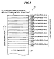
- FIG. 5 is a cross-sectional view schematically showing a constitution of a light-emitting layer having the multiple quantum well structure of a Group III nitride semiconductor light-emitting device (LED) of the second embodiment.
- LED Group III nitride semiconductor light-emitting device
- a light-emitting layer 205 having the multiple quantum well structure shown in FIG. 5 was formed, by nitrogen plasma MBE, on a stacked structure comprising the AlN layer, the AlGaN mixed crystal layer, and the n-type GaN layer (204 in FIG. 5 ) described in the first embodiment and provided on the Si substrate.
- the light-emitting layer 205 was formed as follows.
- an n-type GaN barrier layer 205a having a thickness of 16 nm is first provided on the n-type GaN layer 204 by nitrogen plasma MBE. Then, an Mg doped Ga 0.80 In 0.20 N well layer as an n-type well layer 205b constituting the multiple quantum well structure was provided so that the n-type well layer 205b is joined to this barrier layer 205a. Ten pairs of structural units which each comprise this n-type barrier layer 205a and the n-type well layer 205b are stacked to provide a light-emitting layer 305 having the multiple quantum well structure that has n-type conductivity as a whole.
- the ten well layers 205b constituting the multiple quantum well structure that ten structural units were stacked on top of each other were reduced in thickness in the stacking direction from the n-type GaN layer 204 side toward the surface of the multiple quantum well structure.
- the stacking direction is the same as the direction of taking out light emission of the light-emitting device (LED).
- the lowermost well layer 205b has a thickness of 12 nm
- the well layer 205b provided above the lowermost well layer 205b has a thickness of 11 nm
- the next lowest well layer 205b has a thickness of 10 nm.
- the thickness of the well layer 205b is reduced by 1 nm toward the outermost surface layer of the multiple quantum well structure, and the thickness of the outermost surface layer of the well layers 205b is 3 nm (see, FIG. 5 ).
- Mg was doped in each well layer 205b so that the atomic concentration is 6 ⁇ 10 17 atoms/cm 3 and substantially constant.
- An Mg doped p-type Al 0.03 Ga 0.97 N layer having a thickness of 10 nm was accumulated on an Mg doped Ga 0.80 In 0.20 N well layer 205b (with a thickness of 3 nm), which is the outermost surface layer of the light-emitting layer 205 having the multiple quantum well structure, by nitrogen plasma MBE, whereby the formation of the stacked structure for use in a light-emitting device (LED) was terminated.
- LED light-emitting device
- FIG. 6 shows a photoluminescence spectrum at room temperature obtained from the stacked structure including the light-emitting layer 205 having the multiple quantum well structure.
- the horizontal axis represents emission wavelength (unit: ⁇ ), and the vertical axis represents emission intensity (unit: arbitrary unit).
- the photoluminescence spectrum shown in FIG. 6 is a spectrum obtained by superimposing the multiwavelength emission components from the well layers 205b with different thicknesses. A total of ten emissions were radiated over a wide wavelength range from 400 nm to 800 nm. The difference of the wavelength between the adjacent emissions is 17.5 nm to 78.0 nm, and the interval of the wavelength becomes larger as the emission wavelength becomes longer-wavelength.
- He-Cd helium-cadmium
- the region where an n-type ohmic electrode is formed is removed by a typical dry etching method to form the n-type ohmic electrode. Meanwhile, a p-type ohmic electrode is formed on the surface of the p-type Al 0.03 Ga 0 . 97 N layer, and a light-emitting device (LED) is produced.
- LED light-emitting device
- the forward voltage (Vf) is 3.4 V.
- the LED in a chip state emits light of white color as a visible color.
- FIG. 7 is a schematic cross-sectional view showing a structure of a Group III nitride semiconductor light-emitting device comprising a light-emitting layer having the multiple quantum well structure of a third embodiment.
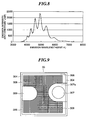
- FIG. 8 is a photoluminescence spectrum in a stacked structure for use in a Group III nitride semiconductor light-emitting device (LED) comprising the light-emitting layer having the multiple quantum well structure of the third embodiment.
- LED Group III nitride semiconductor light-emitting device
- the light-emitting layer having the multiple quantum well structure was formed on the stacked structure that comprises the AlN layer and the AlGaN mixed crystal layer (303 in FIG. 7 ) described in the first and second embodiments and provided on an Si substrate.
- the light-emitting layer is formed as follows.
- an n-type GaN barrier layer 305a with a thickness of 10 nm was first provided on the AlGaN mixed crystal layer 303, described in the first and second embodiments, by nitrogen plasma MBE. Then, an Mg doped n-type Ga 0.75 In 0.25 N well layer 305b with a thickness of 3 nm was provided so as to be joined to the barrier layer 305a. Five pairs of structural units each comprising the n-type barrier layer 305a and the n-type well layer 305b are stacked to provide a light-emitting layer 305 having the multiple quantum well structure that has n-type conductivity as a whole.
- the atomic concentration of Mg contained within the five well layers 305b constituting themultiple quantumwell structure of five structural units stacked on top of each other is reduced from the AlGaN mixed crystal layer 303 side toward the stacking direction (the same as the light taking out direction).
- the atomic concentration of Mg is sequentially reduced so that the atomic concentration of Mg contained within the lowermost well layer 305b is 1 ⁇ 10 19 atoms/cm 3 , the atomic concentrations of Mg contained within the well layers 305b provided above the lowermost well layer 305b are respectively 8 ⁇ 10 18 atoms/cm 3 , 6 ⁇ 10 18 atoms/cm 3 , 4 ⁇ 10 18 atoms/cm 3 , and 2 ⁇ 10 18 atoms/cm 3 .
- This constitution provides the light-emitting layer 305 having the multiple quantum well structure comprising the five well layers 305b, which have different Mg atomic concentrations while each of the well layers 305b has the same thickness.
- An Mg doped p-type GaN layer 306 with a thickness of 10 nm was accumulated on an Mg doped GaN well layer (with an Mg atomic concentration of 2 ⁇ 10 18 atoms/cm 3 ), which is the outermost surface layer of the light-emitting layer 305 having the multiple quantum well structure, by nitrogen plasma MBE, whereby the formation of the stacked structure for use in the light-emitting device (LED) was terminated.
- FIG. 8 shows the photoluminescence spectrum at room temperature obtained from the stacked structure including the light-emitting layer 305 having the multiple quantum well structure.
- the horizontal axis represents emission wavelength (unit: ⁇ ), and the vertical axis represents emission intensity (unit: arbitrary unit).
- the photoluminescence spectrum shown in FIG. 8 is a spectrum obtained by superimposing the multiwavelength emission components from the well layers 305b having a fixed thickness and different Mg atomic concentrations. A total of six emissions were confirmed in a wavelength range from 400 nm to 600 nm, and the respective emission peak wavelengths are 402.5 nm, 429.0 nm, 458.0 nm, 493.0 nm, 538.0 nm, and 593.0 nm.
- the difference of the wavelength between the adjacent emissions is 26.5 nm to 55.0 nm, and the interval of the wavelength becomes larger as the emission wavelength becomes longer-wavelength.
- a helium-cadmium (He-Cd) laser beam (with a wavelength of 325 nm) is irradiated as excitation light, the visually confirmed color of emission from the stacked structure is blue-white.
- FIG. 9 is a plan sectional view of a light-emitting device (LED) 30 produced using the stacked structure of FIG. 7 .
- LED light-emitting device
- the p-type GaN layer 306 and the light-emitting layer 305 having the multiple quantum well structure included in a region 307a in which the n-type ohmic electrode 307 will be formed were removed by a typical dry etching method, whereby the surface of the n-type AlGaN mixed crystal layer 303 provided under the light-emitting layer 305 was exposed. Thereafter, as shown in FIG.
- the n-type ohmic electrode 307 is formed on the exposed surface of the n-type AlGaN mixed crystal layer 303 in the region 307a. Meanwhile, a flat lattice shaped p-type ohmic electrode 308 patterned by utilizing a general photolithographic technique was formed on the surface of the p-type GaN layer 306.
- the p-type ohmic electrode 308 arranged in a lattice form and having a width of 4 ⁇ m was constituted of a metal selected from the platinum (Pt) group making an ohmic contact with the p-type GaN layer 306.
- a pad electrode 309 for bonding is provided at one end of the surface of the p-type GaN layer 306 so as to be electrically connected to the lattice shaped p-type ohmic electrode 308, whereby the light-emitting device (LED) 30 was produced.
- the forward voltage (Vf) is 3.4 V.
- a current of 20 mA is passed in a forward direction, an LED chip having a square shape with a side length of 350 ⁇ m emitted light of white color as a visible color.
- a light-emitting layer has a multiple quantum well structure comprising barrier layers and well layers. According to this constitution, a white light-emitting device can be easily formed with a simple structure, and since the installation area is substantially the same as the plane area of the light-emitting layer, the luminous intensity can be enhanced, whereby the Group III nitride semiconductor light-emitting device with a high industrial applicability can be provided.
Landscapes
- Led Devices (AREA)
Applications Claiming Priority (2)
| Application Number | Priority Date | Filing Date | Title |
|---|---|---|---|
| JP2007251167A JP2009081379A (ja) | 2007-09-27 | 2007-09-27 | Iii族窒化物半導体発光素子 |
| PCT/JP2008/065914 WO2009041237A1 (fr) | 2007-09-27 | 2008-08-28 | Élément semi-conducteur au nitrure iii émettant de la lumière |
Publications (1)
| Publication Number | Publication Date |
|---|---|
| EP2200100A1 true EP2200100A1 (fr) | 2010-06-23 |
Family
ID=40511127
Family Applications (1)
| Application Number | Title | Priority Date | Filing Date |
|---|---|---|---|
| EP08834447A Withdrawn EP2200100A1 (fr) | 2007-09-27 | 2008-08-28 | Élément semi-conducteur au nitrure iii émettant de la lumière |
Country Status (6)
| Country | Link |
|---|---|
| US (1) | US8389975B2 (fr) |
| EP (1) | EP2200100A1 (fr) |
| JP (1) | JP2009081379A (fr) |
| CN (1) | CN101809763B (fr) |
| TW (1) | TW200924246A (fr) |
| WO (1) | WO2009041237A1 (fr) |
Cited By (2)
| Publication number | Priority date | Publication date | Assignee | Title |
|---|---|---|---|---|
| CN103178171A (zh) * | 2013-02-28 | 2013-06-26 | 溧阳市宏达电机有限公司 | 一种高亮度发光二极管 |
| EP4443503A4 (fr) * | 2021-11-30 | 2025-11-12 | Seoul Viosys Co Ltd | Dispositif électroluminescent et module électroluminescent le comprenant |
Families Citing this family (37)
| Publication number | Priority date | Publication date | Assignee | Title |
|---|---|---|---|---|
| JP5229053B2 (ja) | 2009-03-30 | 2013-07-03 | ソニー株式会社 | 信号処理装置、および信号処理方法、並びにプログラム |
| US8742459B2 (en) | 2009-05-14 | 2014-06-03 | Transphorm Inc. | High voltage III-nitride semiconductor devices |
| US8421057B2 (en) * | 2010-06-25 | 2013-04-16 | Invenlux Corporation | Light-emitting devices with improved active-region |
| US8242523B2 (en) * | 2010-07-29 | 2012-08-14 | National Tsing Hua University | III-Nitride light-emitting diode and method of producing the same |
| JP2012089651A (ja) * | 2010-10-19 | 2012-05-10 | Showa Denko Kk | Iii族窒化物半導体素子、多波長発光iii族窒化物半導体層及び多波長発光iii族窒化物半導体層の形成方法 |
| JP2012089678A (ja) * | 2010-10-19 | 2012-05-10 | Showa Denko Kk | Iii族窒化物半導体素子及び多波長発光iii族窒化物半導体層 |
| US8742460B2 (en) | 2010-12-15 | 2014-06-03 | Transphorm Inc. | Transistors with isolation regions |
| US8643062B2 (en) | 2011-02-02 | 2014-02-04 | Transphorm Inc. | III-N device structures and methods |
| US8772842B2 (en) | 2011-03-04 | 2014-07-08 | Transphorm, Inc. | Semiconductor diodes with low reverse bias currents |
| WO2013015035A1 (fr) * | 2011-07-26 | 2013-01-31 | 日亜化学工業株式会社 | Élément électroluminescent à semi-conducteur |
| US8901604B2 (en) | 2011-09-06 | 2014-12-02 | Transphorm Inc. | Semiconductor devices with guard rings |
| US9257547B2 (en) | 2011-09-13 | 2016-02-09 | Transphorm Inc. | III-N device structures having a non-insulating substrate |
| US8598937B2 (en) | 2011-10-07 | 2013-12-03 | Transphorm Inc. | High power semiconductor electronic components with increased reliability |
| CN102412354B (zh) * | 2011-10-29 | 2014-04-16 | 潍坊广生新能源有限公司 | 一种白光led外延结构及制作方法、白光led芯片结构 |
| US8723189B1 (en) * | 2012-01-06 | 2014-05-13 | Trustees Of Boston University | Ultraviolet light emitting diode structures and methods of manufacturing the same |
| US9165766B2 (en) | 2012-02-03 | 2015-10-20 | Transphorm Inc. | Buffer layer structures suited for III-nitride devices with foreign substrates |
| WO2013155108A1 (fr) | 2012-04-09 | 2013-10-17 | Transphorm Inc. | Transistors au nitrure-iii n-polaires |
| US8822314B2 (en) * | 2012-06-14 | 2014-09-02 | Palo Alto Research Center Incorporated | Method of growing epitaxial layers on a substrate |
| US9184275B2 (en) | 2012-06-27 | 2015-11-10 | Transphorm Inc. | Semiconductor devices with integrated hole collectors |
| KR20140019635A (ko) * | 2012-08-06 | 2014-02-17 | 엘지이노텍 주식회사 | 발광 소자 및 발광 소자 패키지 |
| JP6522521B2 (ja) | 2013-02-15 | 2019-05-29 | トランスフォーム インコーポレーテッド | 半導体デバイスの電極及びその製造方法 |
| US9087718B2 (en) | 2013-03-13 | 2015-07-21 | Transphorm Inc. | Enhancement-mode III-nitride devices |
| US9245992B2 (en) | 2013-03-15 | 2016-01-26 | Transphorm Inc. | Carbon doping semiconductor devices |
| US9443938B2 (en) | 2013-07-19 | 2016-09-13 | Transphorm Inc. | III-nitride transistor including a p-type depleting layer |
| US20170125632A1 (en) * | 2014-07-04 | 2017-05-04 | Sharp Kabushiki Kaisha | Nitride-semiconductor light-emitting element |
| US9318593B2 (en) | 2014-07-21 | 2016-04-19 | Transphorm Inc. | Forming enhancement mode III-nitride devices |
| CN104460081A (zh) * | 2014-12-10 | 2015-03-25 | 深圳市华星光电技术有限公司 | 一种液晶显示器和用于其的双面胶带 |
| US9536967B2 (en) | 2014-12-16 | 2017-01-03 | Transphorm Inc. | Recessed ohmic contacts in a III-N device |
| US9536966B2 (en) | 2014-12-16 | 2017-01-03 | Transphorm Inc. | Gate structures for III-N devices |
| CN104834113B (zh) * | 2015-04-29 | 2018-01-16 | 武汉华星光电技术有限公司 | 一种窄边框液晶显示模组 |
| US11322599B2 (en) | 2016-01-15 | 2022-05-03 | Transphorm Technology, Inc. | Enhancement mode III-nitride devices having an Al1-xSixO gate insulator |
| DE102016101442B4 (de) * | 2016-01-27 | 2025-03-13 | OSRAM Opto Semiconductors Gesellschaft mit beschränkter Haftung | Konversionselement und strahlungsemittierendes Halbleiterbauelement mit einem solchen Konversionselement |
| US10224401B2 (en) | 2016-05-31 | 2019-03-05 | Transphorm Inc. | III-nitride devices including a graded depleting layer |
| GB2565055A (en) * | 2017-07-28 | 2019-02-06 | Comptek Solutions Oy | Semiconductor device and manufacturing method |
| JP6645488B2 (ja) * | 2017-11-09 | 2020-02-14 | 信越半導体株式会社 | 半導体型蛍光体 |
| WO2021236732A1 (fr) | 2020-05-19 | 2021-11-25 | Raxium, Inc. | Structure de del à base de puits quantique améliorée avec injection par paroi latérale de trou |
| JP7533335B2 (ja) * | 2021-04-21 | 2024-08-14 | 株式会社デンソー | 光半導体素子および半導体レーザ装置 |
Family Cites Families (33)
| Publication number | Priority date | Publication date | Assignee | Title |
|---|---|---|---|---|
| JPS553834B2 (fr) | 1972-02-26 | 1980-01-26 | ||
| EP0092524B1 (fr) | 1982-04-21 | 1987-08-12 | Ciba-Geigy Ag | Composition de revêtement sensible à la radiation et son application |
| JPH0718357A (ja) | 1991-10-02 | 1995-01-20 | Yasubumi Furuya | 複合機能材料素子 |
| JP2875437B2 (ja) | 1992-07-30 | 1999-03-31 | シャープ株式会社 | 半導体発光素子およびその製造方法 |
| GB2277405A (en) | 1993-04-22 | 1994-10-26 | Sharp Kk | Semiconductor colour display or detector array |
| JPH06314824A (ja) | 1993-04-28 | 1994-11-08 | Toyoda Gosei Co Ltd | Ledモジュール |
| JP2790237B2 (ja) | 1993-06-28 | 1998-08-27 | 日亜化学工業株式会社 | 多色発光素子 |
| JPH0799345A (ja) | 1993-09-28 | 1995-04-11 | Nichia Chem Ind Ltd | 発光ダイオード |
| JP2910023B2 (ja) | 1993-12-24 | 1999-06-23 | 日亜化学工業株式会社 | 窒化ガリウム系化合物半導体発光素子 |
| JPH07235624A (ja) | 1994-02-23 | 1995-09-05 | Toyoda Gosei Co Ltd | Ledランプ |
| JP3351447B2 (ja) | 1994-04-08 | 2002-11-25 | 日亜化学工業株式会社 | Ledディスプレイ |
| JP3329573B2 (ja) | 1994-04-18 | 2002-09-30 | 日亜化学工業株式会社 | Ledディスプレイ |
| JP2979961B2 (ja) | 1994-06-14 | 1999-11-22 | 日亜化学工業株式会社 | フルカラーledディスプレイ |
| JP3637662B2 (ja) * | 1995-12-28 | 2005-04-13 | 豊田合成株式会社 | 3族窒化物半導体発光素子 |
| JP3675044B2 (ja) * | 1996-06-28 | 2005-07-27 | 豊田合成株式会社 | 3族窒化物半導体発光素子 |
| JP3543498B2 (ja) * | 1996-06-28 | 2004-07-14 | 豊田合成株式会社 | 3族窒化物半導体発光素子 |
| TW383508B (en) | 1996-07-29 | 2000-03-01 | Nichia Kagaku Kogyo Kk | Light emitting device and display |
| JP2927279B2 (ja) | 1996-07-29 | 1999-07-28 | 日亜化学工業株式会社 | 発光ダイオード |
| JP2900928B2 (ja) | 1997-10-20 | 1999-06-02 | 日亜化学工業株式会社 | 発光ダイオード |
| JP3978858B2 (ja) * | 1998-04-03 | 2007-09-19 | 松下電器産業株式会社 | 窒化ガリウム系化合物半導体発光素子 |
| US6608330B1 (en) * | 1998-09-21 | 2003-08-19 | Nichia Corporation | Light emitting device |
| JP3454200B2 (ja) * | 1998-09-21 | 2003-10-06 | 日亜化学工業株式会社 | 発光素子 |
| JP4005275B2 (ja) | 1999-08-19 | 2007-11-07 | 日亜化学工業株式会社 | 窒化物半導体素子 |
| JP2001156328A (ja) * | 1999-11-30 | 2001-06-08 | Hitachi Cable Ltd | 発光素子用エピタキシャルウェハおよび発光素子 |
| JP4044261B2 (ja) | 2000-03-10 | 2008-02-06 | 株式会社東芝 | 半導体発光素子及びその製造方法 |
| JP2002176198A (ja) | 2000-12-11 | 2002-06-21 | Mitsubishi Cable Ind Ltd | 多波長発光素子 |
| JP4292925B2 (ja) | 2003-09-16 | 2009-07-08 | 豊田合成株式会社 | Iii族窒化物系化合物半導体発光素子の製造方法 |
| JP3724490B2 (ja) | 2004-01-19 | 2005-12-07 | 日亜化学工業株式会社 | 発光ダイオード |
| JP2006074010A (ja) * | 2004-08-05 | 2006-03-16 | Matsushita Electric Ind Co Ltd | 半導体レーザおよびその製造方法 |
| US7323721B2 (en) * | 2004-09-09 | 2008-01-29 | Blue Photonics Inc. | Monolithic multi-color, multi-quantum well semiconductor LED |
| JP2006114886A (ja) | 2004-09-14 | 2006-04-27 | Showa Denko Kk | n型III族窒化物半導体積層構造体 |
| JP3724498B2 (ja) | 2004-09-27 | 2005-12-07 | 日亜化学工業株式会社 | 発光ダイオード |
| JP2007184346A (ja) * | 2006-01-05 | 2007-07-19 | Kyocera Corp | 発光素子及びその製造方法 |
-
2007
- 2007-09-27 JP JP2007251167A patent/JP2009081379A/ja active Pending
-
2008
- 2008-08-28 CN CN2008801088582A patent/CN101809763B/zh not_active Expired - Fee Related
- 2008-08-28 WO PCT/JP2008/065914 patent/WO2009041237A1/fr not_active Ceased
- 2008-08-28 EP EP08834447A patent/EP2200100A1/fr not_active Withdrawn
- 2008-08-28 US US12/680,705 patent/US8389975B2/en not_active Expired - Fee Related
- 2008-09-24 TW TW097136566A patent/TW200924246A/zh unknown
Non-Patent Citations (1)
| Title |
|---|
| See references of WO2009041237A1 * |
Cited By (3)
| Publication number | Priority date | Publication date | Assignee | Title |
|---|---|---|---|---|
| CN103178171A (zh) * | 2013-02-28 | 2013-06-26 | 溧阳市宏达电机有限公司 | 一种高亮度发光二极管 |
| CN103178171B (zh) * | 2013-02-28 | 2015-08-05 | 溧阳市宏达电机有限公司 | 一种高亮度发光二极管 |
| EP4443503A4 (fr) * | 2021-11-30 | 2025-11-12 | Seoul Viosys Co Ltd | Dispositif électroluminescent et module électroluminescent le comprenant |
Also Published As
| Publication number | Publication date |
|---|---|
| US20100288998A1 (en) | 2010-11-18 |
| JP2009081379A (ja) | 2009-04-16 |
| CN101809763B (zh) | 2012-05-23 |
| US8389975B2 (en) | 2013-03-05 |
| TW200924246A (en) | 2009-06-01 |
| CN101809763A (zh) | 2010-08-18 |
| WO2009041237A1 (fr) | 2009-04-02 |
Similar Documents
| Publication | Publication Date | Title |
|---|---|---|
| US8389975B2 (en) | Group III nitride semiconductor light-emitting device | |
| Schlotter et al. | Fabrication and characterization of GaN/InGaN/AlGaN double heterostructure LEDs and their application in luminescence conversion LEDs | |
| US6329676B1 (en) | Flat panel solid state light source | |
| JP3543498B2 (ja) | 3族窒化物半導体発光素子 | |
| US8470618B2 (en) | Method of manufacturing a light-emitting diode having electrically active and passive portions | |
| US7884351B2 (en) | Nitride semiconductor light-emitting device | |
| KR101611412B1 (ko) | 발광 소자 | |
| US20040056258A1 (en) | Multi-wavelength luminous element | |
| US20100288999A1 (en) | Group iii nitride semiconductor light-emitting device | |
| US20090108276A1 (en) | High Efficiency Dilute Nitride Light Emitting Diodes | |
| JP2002252371A (ja) | 半導体発光装置 | |
| CN102067338A (zh) | 用于产生任意颜色的半导体发光器件 | |
| JP2005268770A (ja) | 白色発光素子及び白色光源 | |
| JP5263881B2 (ja) | Iii族窒化物半導体発光素子 | |
| JP2003037291A (ja) | 発光素子 | |
| CN1166009C (zh) | 用于产生混合色电磁辐射的半导体元件 | |
| KR102399381B1 (ko) | 발광소자 | |
| JP2003332619A (ja) | 半導体発光素子 | |
| JP2009105423A (ja) | Iii族窒化物半導体発光素子 | |
| JPH10144961A (ja) | 半導体発光素子 | |
| JP2003197969A (ja) | GaN系半導体発光素子およびそれを用いた発光装置 | |
| JP3747867B2 (ja) | pn接合型化合物半導体発光素子、その製造方法、ランプ及び光源 | |
| JP2009088553A (ja) | Iii族窒化物半導体層、発光層およびiii族窒化物半導体発光素子 | |
| KR200410859Y1 (ko) | 3원색 다중발광 양자우물층이 포함된 백색 조명램프 | |
| KR100545441B1 (ko) | 발광기판led소자 |
Legal Events
| Date | Code | Title | Description |
|---|---|---|---|
| PUAI | Public reference made under article 153(3) epc to a published international application that has entered the european phase |
Free format text: ORIGINAL CODE: 0009012 |
|
| 17P | Request for examination filed |
Effective date: 20100423 |
|
| AK | Designated contracting states |
Kind code of ref document: A1 Designated state(s): AT BE BG CH CY CZ DE DK EE ES FI FR GB GR HR HU IE IS IT LI LT LU LV MC MT NL NO PL PT RO SE SI SK TR |
|
| AX | Request for extension of the european patent |
Extension state: AL BA MK RS |
|
| DAX | Request for extension of the european patent (deleted) | ||
| STAA | Information on the status of an ep patent application or granted ep patent |
Free format text: STATUS: THE APPLICATION HAS BEEN WITHDRAWN |
|
| 18W | Application withdrawn |
Effective date: 20130826 |