EP2201821B1 - Circuit permettant de faire fonctionner des diodes électroluminescentes et procédé permettant de faire fonctionner des diodes électroluminescentes - Google Patents
Circuit permettant de faire fonctionner des diodes électroluminescentes et procédé permettant de faire fonctionner des diodes électroluminescentes Download PDFInfo
- Publication number
- EP2201821B1 EP2201821B1 EP08840612.9A EP08840612A EP2201821B1 EP 2201821 B1 EP2201821 B1 EP 2201821B1 EP 08840612 A EP08840612 A EP 08840612A EP 2201821 B1 EP2201821 B1 EP 2201821B1
- Authority
- EP
- European Patent Office
- Prior art keywords
- current value
- current
- switch
- phase
- control unit
- Prior art date
- Legal status (The legal status is an assumption and is not a legal conclusion. Google has not performed a legal analysis and makes no representation as to the accuracy of the status listed.)
- Not-in-force
Links
Images


Classifications
-
- H—ELECTRICITY
- H05—ELECTRIC TECHNIQUES NOT OTHERWISE PROVIDED FOR
- H05B—ELECTRIC HEATING; ELECTRIC LIGHT SOURCES NOT OTHERWISE PROVIDED FOR; CIRCUIT ARRANGEMENTS FOR ELECTRIC LIGHT SOURCES, IN GENERAL
- H05B45/00—Circuit arrangements for operating light-emitting diodes [LED]
- H05B45/10—Controlling the intensity of the light
- H05B45/14—Controlling the intensity of the light using electrical feedback from LEDs or from LED modules
-
- H—ELECTRICITY
- H05—ELECTRIC TECHNIQUES NOT OTHERWISE PROVIDED FOR
- H05B—ELECTRIC HEATING; ELECTRIC LIGHT SOURCES NOT OTHERWISE PROVIDED FOR; CIRCUIT ARRANGEMENTS FOR ELECTRIC LIGHT SOURCES, IN GENERAL
- H05B45/00—Circuit arrangements for operating light-emitting diodes [LED]
- H05B45/30—Driver circuits
- H05B45/37—Converter circuits
- H05B45/3725—Switched mode power supply [SMPS]
Definitions
- the present invention relates to a circuit and a method for operating light-emitting diodes by means of switching regulators for providing the operating voltage for the LEDs.
- a control unit controls a clocked semiconductor power switch, by means of which an inductance is energized in its on state, wherein the energy of the inductor then discharges in the off state of the switch via the light emitting diode path.
- a driving circuit for lighting means which allows switching of a switch depending on a LED current.
- the time average of the LED current by appropriate timing of the circuit breaker be set.
- the current through the light-emitting diodes must therefore also be detected.
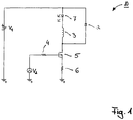
- Fig. 1 is shown schematically an example of a circuit for controlled operation of light-emitting diodes.
- a circuit for controlled operation of light-emitting diodes In the example shown here according to Fig. 1 is shown as a basic circuit for LED modules, a first buck converter 10.
- V 1 For the operation of at least one light emitting diode 7 of the circuit, an input DC voltage V 1 is supplied, which of course can also be a rectified AC voltage.
- a series connection between a switch 5, for example a semiconductor power switch, in particular a MOSFET, and a freewheeling diode 2 energizes in the switched-on state of the switch 5 an inductance 3 by means of the current flowing through the switch 5 current.
- the energy stored in the inductance 3 discharges in the form of a current through the at least one light-emitting diode 7
- the current flowing through the at least one light-emitting diode 7 current can be measured at a shunt resistor 6 by a corresponding sensor.
- the disadvantage here is that at the shunt resistor 6, the current can be measured only during the switch-on of the switch 5.
- the current flows through the freewheeling diode 2, the at least one light-emitting diode 7 and the inductance 3 and is not detectable for a sensor connected to the shunt resistor 6.
- the present invention relates to an operating circuit for at least one light-emitting diode, comprising a switching regulator circuit, which is supplied with a DC voltage and provides a supply voltage for the at least one light-emitting diode by means of a clocked by a control unit switch, and one with the control unit connected current sensor for detecting the current flowing through the at least one light emitting diode during the switch-on of the switch, wherein the control unit determines the time duration between a switch off and a subsequent switching on of the switch depending on the current detected by the current sensor during the switch-on.
- the control unit is designed to calculate, based on an increase of the current detected by the current sensor during the switch-on phase, a period of time between a switch-off and a subsequent switch-on of the switch, which is necessary to reach a certain current value at the end of a freewheeling phase.
- the control unit (13) can calculate the current value (I A ) at the end of the freewheeling phase (F) of the switch (5) by means of at least one current value detected by the current sensor (6, 12).
- the control unit (13) can compare the calculated current value (IA) at the end of the freewheeling phase (F) with a predetermined desired value.
- the control unit can not change the time duration (toff) between switching off and subsequent switching on of the switch (5) if the calculated current value (IA) at the end of the free-running phase (F) corresponds to the desired value.
- the control unit may increase the time duration (toff) between a switch-off and a subsequent switch-on of the switch (5) if the calculated current value (IA) at the end of the free-running phase (F) is greater than the setpoint value.
- the control unit may reduce the time (toff) between turning off and subsequently turning on the switch (5) if the calculated current value (IA) is less than the setpoint at the end of the free running phase (F).
- the present invention further relates to a method for operating at least one light-emitting diode by means of a switching regulator circuit, which is supplied with a DC voltage and provides a supply voltage for the at least one light-emitting diode by means of a clocked switch, comprising the steps of detecting the light emitted by the at least one light-emitting diode (LED). flowing current during the switch-on phase of the switch and determining the time duration between a switch-off and a subsequent switch-on of the switch depending on the current detected during the switch-on phase. Based on an increase of the current detected during the switch-on phase, a time period between a turn-off and a subsequent turn-on of the switch is calculated, which is necessary to reach a certain current value at the end of a freewheeling phase.
- a switching regulator circuit which is supplied with a DC voltage and provides a supply voltage for the at least one light-emitting diode by means of a clocked switch, comprising the steps of detecting the light
- control unit calculates the current value at the end of the freewheeling phase of the switch by means of at least one current value detected by the current sensor.
- control unit compares the calculated current value at the end of the freewheeling phase with a predetermined desired value.
- control unit advantageously does not change the time duration between a switch-off and a subsequent switch-on of the switch if the calculated current value at the end of the free-running phase corresponds to the setpoint value.
- control unit increases the time duration between a switch-off and a subsequent switching-on of the switch if the calculated current value at the end of the free-running phase is greater than the setpoint value.
- control unit advantageously increases the time duration between a switching off and a subsequent switching on of the switch if the calculated current value at the end of the freewheeling phase is less than the setpoint value.
- the control unit waits for a fade-out time t blk and detects a first current value immediately after the fade-out time by means of the current sensor.
- I A is the current value at the end of the freewheeling phase
- I B is the first current value
- I D is the second current value.
- I A is the current value at the end of the freewheeling phase
- I B is the first current value
- I C is the third current value.
- control unit determines the time duration between switching off and subsequent switching on of the switch as a function of the rise in the current detected by the current sensor during the switch-on phase.
- Fig. 2 shows the typical voltage and current waveforms in a Buck converter, or in the case of a square-wave voltage.
- the time is shown along the X-axis and along the Y-axis of the voltage curve or the current waveform through the at least one light emitting diode. 7
- the operating circuit is supplied with a Recheckbeginn, ie during the switch-on phase E of the switch 5 over a period of time t on the operating circuit is supplied with a certain voltage, and during a freewheeling phase F over a period of time t Off , during which the Switch 5 is open, the circuit is not powered by the voltage source.
- the inductance 3 results in the at least one light emitting diode 7, a current waveform as in Fig. 2 shown.
- the current through the at least one light-emitting diode 7 increases and during the following free-wheeling phase F the current through the at least one sinks LED 7 off again.
- a current spike arises. After its decay, the current increases linearly due to the inductance 3.
- the inductance over the load and the diode 2 is free.
- the time duration during the current peak is referred to as blanking time t blk or as blanking time t blk .
- the present invention circumvents this problem by detecting the current directly after the switch 5 is turned on and by deducing the freewheeling current through the measured values of the current during the switch-on time E.
- Fig. 3 shows an operating circuit 1 according to the invention for the operation of at least one light emitting diode 7.
- the circuit corresponds to the first buck converter 11, as in Fig. 1 is shown and has already been explained.
- a sensor 12 is additionally provided here, which is suitable for detecting the current measured by means of the shunt resistor 6 and for detecting the current Pass value to a control unit 13.
- the control unit 13 actuates the switch 5 and is furthermore suitable for correspondingly determining the switch-off duration t Off and the switch-on time t On of the switch 5 on the basis of the measured current values transmitted by the sensor 12.
- the determination of the switch-off period t Off by the control unit 13 will be explained in detail below.
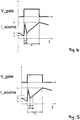
- Fig. 4 is again the voltage and current waveform shown in a light emitting diode module.
- a first possibility to be able to infer the current I A at the end of the freewheeling time is, after the blanking time, ie the blanking time t blk , to measure a first current value I B.
- t blk is much smaller than t on and thus the current I B measured after the blanking time corresponds approximately to the current I A at the end of the freewheeling time.
- the current value thus calculated at the end of the freewheeling phase I A is compared with a setpoint value and if I A is greater than the desired setpoint value, then the time period t Off between a switch-off and a subsequent switch-on is increased at the next cycle. If the current I A is smaller than the desired reference value, then t Off is shortened at the next cycle. If the current I A also corresponds to the desired setpoint value within predetermined tolerance values, t Off is left unchanged at the next cycle.
- This calculation is based on the principle that the current after switching on the switch 5 increases linearly and thus can be calculated back by two measurements of the current waveform I B and I D to the current I A at the end of the freewheeling phase.
- a third method is proposed which is based on the measurement of a third current value I c .
- This is schematically in Fig. 5 shown.
- the current value I A can be calculated relatively easily at the end of the freewheeling phase, since the calculation in the digital domain is reduced to a bit shift as well as a subtraction.
- the present invention it is ensured that the current flow through the at least one light-emitting diode 7 as possible never drops to zero, d. H.
- the invention relates in particular to the continuous conduction mode. This results in the smallest possible ripple of the current flow through the at least one light emitting diode. 7
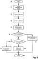
- step S0 the control unit 13 outputs the signal for the switch-on phase to the switch 5.
- step S2 the blanking time, ie the blanking time t blk is waited.
- step S3 which also consists of several
- step S4 the control unit calculates the return current based on the transmitted current values, ie the current I A at the end of the freewheeling phase.
- step S5 it is checked whether the return current corresponds to a predetermined desired value. If this is the case, no change in the switch-off time t Off is made in the following step S7.
- step S5 if it is determined in step S5 that the return current I A does not correspond to a desired value, it is checked in the following step S6 whether the return current I A is greater than the desired value. If so, in a following step S9 the next off time is increased, otherwise in a following step S8 the following off time is reduced.
- the turn-off time is the time period between the turn-off and the subsequent turn-on of the switch 5. The process ends in step S10.
- step S4 can in this case be based on one of the three methods mentioned, depending on the presettings and the recorded measured values.
- Another possibility of the regulation is that the increase in the current value detected by the current sensor 6, 12 is evaluated. The difference between the current value at the beginning and at the end of the switch-on phase is determined. From the rise of the current can be closed to the size of the inductor 3 or the forward voltage of the LED 7. If the size of the inductor 3 or the forward voltage of the LED 7 are known, can be closed to the required for reaching a return current I A off time t off .
- the current through the switch S results from the quotient of voltage across the inductance 3 and the value of the inductance 3 multiplied by the switch-on time.
- the drop in the current in the freewheeling path results from the quotient of voltage across the inductance 3 and the value of the inductance 3 multiplied by the switch-off time. Since, during the freewheeling phase, the voltage across the inductance approximately corresponds to the voltage across the light emitting diode 7 (the difference results from the forward voltage of the freewheeling diode 2).
- both the forward voltage of the light-emitting diodes 7 and the inductance 3 can be determined over the duration of switch-on phase E and switch- off phase F and by measuring the switch-on time and switch-off time t off .
- the Determination of the required switch-off time simplified. But it is also possible to measure the voltage across the inductor 3 or the LED 7 during operation.
- the switch S is turned on, according to the circuit Fig. 3 the voltage across the inductance 3 can be measured via a voltage measurement at the connection point between the inductance 3 and the light-emitting diode 7. If both components are interchanged, the forward voltage across the light emitting diode 7 can be measured in a simple manner. Such a voltage measurement can also be used for fault detection. Thus, for example, an error of the light-emitting diode 7 or even a fault caused by a fault in the wiring of the light-emitting diode 7 such as a short circuit can be concluded.
- a temporal monitoring of the detected current values can be carried out. If a change in the detected current values is detected, it is possible to infer a possible fault or also an aging of the light-emitting diode 7 or of other components.
- the determination of the inductance 3 or the Flux voltage of the LED 7 can be corrected or completed.
- the required time duration t off which is necessary to reach a specific current value I A at the end of the freewheeling phase F, can be calculated.
- the actually achieved current value I A at the end of the freewheeling phase F can then be compared with a predefined setpoint value and the time period t off can be adjusted again.
- Such a digital circuit advantageously has at least one analog-to-digital converter for detecting the current and voltage values, a computing block for processing and calculating the corresponding values, and a memory register for storing the measured values and calculated values.
- An advantageous design of the operating circuit according to the invention can be designed so that only the current during the switch-on phase is measured and evaluated for the regulation of the current through the light emitting diode 7, while an existing voltage detection is used only for an error shutdown.
- a comparator for monitoring the voltage of the light emitting diode 7 or the voltage across the inductance 3 can be used, whereby a cost-effective circuit can be constructed.
- Fig. 7 shows a further operating circuit 1 according to the invention for the operation of at least one light emitting diode 7.
- the circuit corresponds to a buck-boost converter 110.
- the current is measured by the shunt resistor 6 through the switch 5 and the value is forwarded to a control unit 13.
- the control unit 13 actuates the switch 5 and is furthermore suitable, on the basis of the measured current values transmitted by the shunt resistor 6, to correspondingly determine the switch-off time duration t Off and the switch-on time duration t On of the switch 5.
- the inductance 3 is magnetized.
- the switch-off phase F over a period of time toff, the inductance 3 is demagnetized, the current flowing through the light-emitting diode 7 and the diode 2.
- the inventive method can be used for all circuit topologies for the operation of LEDs, where no direct measurement of the current through the LEDs is possible because the LEDs are not directly connected to ground, but are connected to a variable with respect to ground potential.
- This method can therefore also be used in operating circuits with potential separation, wherein during a switch-on phase E an inductance 3 is magnetized and is demagnetized in a subsequent switch-off phase F while driving a current through at least one light emitting diode 7.
- the inductance 3 may be a secondary winding through which it outputs its energy during the turn-off phase F, whereby the potential separation is achieved in the circuit.
- Such a circuit may be, for example, a forward converter.
- the current is detected and evaluated by a switch (and the current increase) during a switch-on phase E and determines the necessary switching behavior of the switch 5 (for example, the (switch-off) time period t off )
- the present operating circuit and the present method for operating at least one light-emitting diode thus results that regardless of the load, for example, regardless of the number of light-emitting diodes supplied, the current waveform is always maintained between a value I max and a value Imin, ie always at the same Value I min > 0, the switch 5 is switched on again.
- An advantage of the relatively small ripple guaranteed by the invention ie the difference between Imin and I max , ie I min -I max , is that the light-emitting diode is essentially supplied with a constant current, so that the color shift is very different Light-emitting diode currents does not show. This is a disadvantage of circuits that operate in discontinuous mode, ie where the LED current drops to zero and possibly even a time remains at zero before the switch is turned on again.
Landscapes
- Circuit Arrangement For Electric Light Sources In General (AREA)
- Dc-Dc Converters (AREA)
- Led Devices (AREA)
Claims (12)
- Circuit d'actionnement pour au moins une diode électroluminescente (7), comprenant
un circuit régulateur auquel est appliqué une tension continue et qui génère une tension d'alimentation pour l'au moins une diode électroluminescente (7) au moyen d'un commutateur (5) cadencé par une unité de commande (13) et
un capteur de courant (6, 12) relié avec l'unité de commande (13) pour la mesure du courant s'écoulant à travers l'au moins une diode électroluminescente (7) pendant la phase d'activation (E) du commutateur (5),
caractérisé en ce que
l'unité de commande (13) est conçu pour calculer, à l'aide d'une augmentation du courant mesuré au moyen du capteur de courant (6, 12) pendant la phase d'activation (E), une période (toff) entre une désactivation et une activation suivante du commutateur (5), qui est nécessaire pour atteindre une valeur de courant (IA) déterminée à la fin d'une phase de roue libre (F). - Circuit (1) selon la revendication 1,
l'unité de commande (13) attendant, à compter de la phase d'activation (E) du commutateur (5), un temps de masquage (tblk) et, immédiatement après le temps de masquage (tblk), mesurant une première valeur de courant (IB) au moyen du capteur de courant (6, 12). - Circuit (1) selon la revendication 2,
l'unité de commande (13) calculant la valeur de courant (IA) à la fin de la phase de roue libre (F) au moyen de la première valeur de courant (IB), à l'aide de l'équation :
- Circuit (1) selon la revendication 2,
l'unité de commande (13) déterminant une deuxième valeur de courant (ID) à la fin de la phase d'activation (E) et
l'unité de commande (13) calculant la valeur de courant (IA) à la fin de la phase de roue libre (F) au moyen de la première (IB) et de la deuxième valeur de courant (ID), à partir de
- Circuit (1) selon la revendication 2,
l'unité de commande attendant, après la mesure de la première valeur de courant (IB), à nouveau la durée du temps de masquage (tblk) et mesurant, immédiatement après le deuxième temps de masquage (tblk), une troisième valeur de courant (IC) et l'unité de commande (13) calculant la valeur de courant (IA) à la fin de la phase de roue libre (F) au moyen de la première (IB) et de la troisième valeur de courant (IC), à partir de
- Procédé d'actionnement d'au moins une diode électroluminescente (7) au moyen d'un circuit régulateur auquel est appliquée une tension continue et qui génère, au moyen d'un commutateur cadencé (5), une tension d'alimentation pour l'au moins une diode électroluminescente (7), comprenant l'étape de :- mesure du courant s'écoulant à travers l'au moins une diode électroluminescente (7) (LED) pendant la phase d'activation (E) du commutateur (5),caractérisé en ce que
à l'aide d'une augmentation du courant mesuré pendant la phase d'activation (E), une période (toff) est mesurée entre une désactivation et une activation suivante du commutateur (5), nécessaire pour atteindre une valeur de courant (IA) prédéterminée à la fin d'une phase de roue libre (F). - Procédé selon la revendication 6,
la période (toff) entre la désactivation et une activation suivante du commutateur (5) étant déterminée en fonction de l'augmentation du courant mesuré au moyen du capteur de courant (6, 12) pendant la phase d'activation (E). - Procédé selon la revendication 6 ou 7,
l'unité de commande augmentant la période (toff) entre une désactivation et une activation suivante du commutateur (5) si la valeur de courant (IA) calculée à la fin de la phase de roue libre (F) est supérieure à la valeur de consigne,
et/ou
diminue cette période si la valeur de courant calculée est inférieure à la valeur de consigne. - Procédé selon l'une des revendications 6 à 8,
l'unité de commande (13) attendant, à compter de la phase d'activation (E) du commutateur (5), un temps de masquage (tblk) et mesurant, immédiatement après le temps de masquage (tblk), une première valeur de courant (IB) au moyen du capteur de courant (6, 12). - Procédé selon la revendication 9,
l'unité de commande (13) calculant la valeur de courant (IA) à la fin de la phase de roue libre (F) au moyen de la première valeur de courant (IB), à l'aide de
IA = IB,
IA étant la valeur de courant à la fin de la phase de roue libre (F) et IB étant la première valeur de courant. - Procédé selon la revendication 9,
l'unité de commande (13) déterminant une deuxième valeur de courant (ID) à la fin de la phase d'activation (E) et
l'unité de commande (13) calculant la valeur de courant (IA) à la fin de la phase de roue libre (F) au moyen de la première et de la deuxième valeur de courant (ID), à partir de
- Procédé selon la revendication 9,
l'unité de commande attendant, après la mesure de la première valeur de courant (IB), à nouveau la durée du temps de masquage (tblk) et mesurant, immédiatement après le deuxième temps de masquage (tblk), une troisième valeur de courant (IC) et
l'unité de commande (13) calculant la valeur de courant (IA) à la fin de la phase de roue libre (F) au moyen de la première (IB) et de la troisième valeur de courant (IC), à partir de
Applications Claiming Priority (2)
| Application Number | Priority Date | Filing Date | Title |
|---|---|---|---|
| DE102007049533.3A DE102007049533B4 (de) | 2007-10-16 | 2007-10-16 | Betriebsschaltung für Leuchtdioden und Verfahren zum Betrieb von Leuchtdioden |
| PCT/EP2008/008729 WO2009049876A2 (fr) | 2007-10-16 | 2008-10-15 | Circuit permettant de faire fonctionner des diodes électroluminescentes et procédé permettant de faire fonctionner des diodes électroluminescentes |
Publications (2)
| Publication Number | Publication Date |
|---|---|
| EP2201821A2 EP2201821A2 (fr) | 2010-06-30 |
| EP2201821B1 true EP2201821B1 (fr) | 2017-09-13 |
Family
ID=40458730
Family Applications (1)
| Application Number | Title | Priority Date | Filing Date |
|---|---|---|---|
| EP08840612.9A Not-in-force EP2201821B1 (fr) | 2007-10-16 | 2008-10-15 | Circuit permettant de faire fonctionner des diodes électroluminescentes et procédé permettant de faire fonctionner des diodes électroluminescentes |
Country Status (5)
| Country | Link |
|---|---|
| EP (1) | EP2201821B1 (fr) |
| CN (1) | CN101828428A (fr) |
| AT (1) | AT516957B1 (fr) |
| DE (1) | DE102007049533B4 (fr) |
| WO (1) | WO2009049876A2 (fr) |
Families Citing this family (4)
| Publication number | Priority date | Publication date | Assignee | Title |
|---|---|---|---|---|
| DE102009027484A1 (de) | 2009-07-06 | 2011-01-13 | Osa Opto Light Gmbh | Schaltungsanordnung zur Dimmung einer Leuchtquelle, die wengistens ein strahlungsemittierendes Halbleiterbauelement umfasst |
| DE102011088966A1 (de) * | 2011-12-19 | 2013-06-20 | Tridonic Gmbh & Co. Kg | Betriebsschaltung für Leuchtdioden und Verfahren zum Betrieb von Leuchtdioden |
| AT13857U1 (de) * | 2013-04-30 | 2014-10-15 | Tridonic Gmbh & Co Kg | Fehlererkennung für Leuchtdioden |
| WO2021246044A1 (fr) * | 2020-06-04 | 2021-12-09 | パナソニックIpマネジメント株式会社 | Circuit de dispositif de commutation, système de commutation et procédé de traitement de dispositif de commutation |
Family Cites Families (4)
| Publication number | Priority date | Publication date | Assignee | Title |
|---|---|---|---|---|
| FI106770B (fi) * | 1999-01-22 | 2001-03-30 | Nokia Mobile Phones Ltd | Valaiseva elektroninen laite ja valaisumenetelmä |
| US20050151708A1 (en) * | 2004-01-12 | 2005-07-14 | Farmer Ronald E. | LED module with uniform LED brightness |
| US7378805B2 (en) * | 2005-03-22 | 2008-05-27 | Fairchild Semiconductor Corporation | Single-stage digital power converter for driving LEDs |
| US7259525B2 (en) * | 2005-11-03 | 2007-08-21 | System General Corporation | High efficiency switching LED driver |
-
2007
- 2007-10-16 DE DE102007049533.3A patent/DE102007049533B4/de not_active Expired - Fee Related
-
2008
- 2008-10-15 EP EP08840612.9A patent/EP2201821B1/fr not_active Not-in-force
- 2008-10-15 WO PCT/EP2008/008729 patent/WO2009049876A2/fr not_active Ceased
- 2008-10-15 CN CN200880112068A patent/CN101828428A/zh active Pending
- 2008-10-15 AT ATA9322/2008A patent/AT516957B1/de not_active IP Right Cessation
Non-Patent Citations (1)
| Title |
|---|
| None * |
Also Published As
| Publication number | Publication date |
|---|---|
| WO2009049876A2 (fr) | 2009-04-23 |
| EP2201821A2 (fr) | 2010-06-30 |
| WO2009049876A3 (fr) | 2009-07-23 |
| AT516957A5 (de) | 2016-10-15 |
| WO2009049876A9 (fr) | 2009-06-11 |
| DE102007049533B4 (de) | 2017-02-23 |
| DE102007049533A1 (de) | 2009-04-23 |
| CN101828428A (zh) | 2010-09-08 |
| AT516957B1 (de) | 2016-10-15 |
Similar Documents
| Publication | Publication Date | Title |
|---|---|---|
| EP2340688B1 (fr) | Circuit pour faire fonctionner au moins une del | |
| DE102006034371B4 (de) | Betriebsschaltung und Betriebsverfahren für Leuchtdioden | |
| DE102015102101A1 (de) | Phasenfehlererkennung in schaltleistungswandlern | |
| DE102015105488A1 (de) | System und verfahren für eine getaktete leistungsversorgung | |
| DE102012007477A1 (de) | Verfahren zum Betreiben eines LLC-Resonanzwandlers für ein Leuchtmittel, Wandler und LED-Konverter | |
| DE102017115474A1 (de) | System und Verfahren zum Steuern von Strom in einem Schaltregler | |
| EP3114898B1 (fr) | Led-driver | |
| DE102022112757B4 (de) | Intelligenter halbleiterschalter mit integrierter strommessfunktion | |
| DE102013219153B4 (de) | Treibermodul mit sekundärseitiger Erkennung einer primärseitigen elektrischen Versorgung | |
| AT516957B1 (de) | Betriebsschaltung für leuchtdioden und verfahren zum betrieb von leuchtdioden | |
| DE102010002226A1 (de) | Verfahren und Schaltung zur Leistungsfaktor-Korrektur | |
| DE102016118951B4 (de) | Elektronische Steuerung mit automatischer Anpassung an unbekannte Eingangs- und Lastspannungen sowie Verfahren hierzu | |
| DE102017221657A1 (de) | Verfahren zum Durchführen eines Selbsttests einer elektrischen Wandlerschaltung sowie Wandlerschaltung und Fahrzeugleuchte | |
| EP3307022B1 (fr) | Circuit convertisseur flyback cadencé | |
| DE102014201973B4 (de) | Elektromagnetventilansteuervorrichtung | |
| DE102014223377B4 (de) | Betriebsschaltung zur Versorgung eines Leuchtmittels, LED-Konverter, System und Verfahren zum Betreiben einer Betriebsschaltung | |
| DE10108877A1 (de) | Entladungslampenversorgungsschaltung | |
| EP3791692B1 (fr) | Circuit convertisseur à transfert indirect synchrone pour faire fonctionner une section de moyens d'éclairage | |
| DE102016208183A1 (de) | Konverterschaltung für Leuchtmittel mit einem Messpunkt zur Erfassung kombinierter elektrischer Parameter | |
| DE102015203950A1 (de) | Betriebsgerät mit Erkennung des Wegfalls der Versorgungsspannung | |
| EP2849538B1 (fr) | Dispositif et procédé de détermination indirecte d'une alimentation électrique | |
| EP2702676B1 (fr) | Procédé et dispositif de correction du facteur de puissance | |
| EP2425684B1 (fr) | Circuit de ballast régulé en puissance pour un luminaire, et procédé de fonctionnement | |
| AT18055U1 (de) | Sperrwandler zum Betreiben von einem oder mehreren Leuchtmitteln, dazugehöriges Verfahren und Betriebsgerät | |
| AT14104U1 (de) | Betriebsschaltung für eine Leuchtdiode und Verfahren zum Steuern einer Betriebsschaltung |
Legal Events
| Date | Code | Title | Description |
|---|---|---|---|
| PUAI | Public reference made under article 153(3) epc to a published international application that has entered the european phase |
Free format text: ORIGINAL CODE: 0009012 |
|
| 17P | Request for examination filed |
Effective date: 20100208 |
|
| AK | Designated contracting states |
Kind code of ref document: A2 Designated state(s): AT BE BG CH CY CZ DE DK EE ES FI FR GB GR HR HU IE IS IT LI LT LU LV MC MT NL NO PL PT RO SE SI SK TR |
|
| AX | Request for extension of the european patent |
Extension state: AL BA MK RS |
|
| RAP1 | Party data changed (applicant data changed or rights of an application transferred) |
Owner name: TRIDONIC GMBH & CO KG |
|
| DAX | Request for extension of the european patent (deleted) | ||
| 17Q | First examination report despatched |
Effective date: 20120126 |
|
| GRAP | Despatch of communication of intention to grant a patent |
Free format text: ORIGINAL CODE: EPIDOSNIGR1 |
|
| STAA | Information on the status of an ep patent application or granted ep patent |
Free format text: STATUS: GRANT OF PATENT IS INTENDED |
|
| INTG | Intention to grant announced |
Effective date: 20170608 |
|
| GRAS | Grant fee paid |
Free format text: ORIGINAL CODE: EPIDOSNIGR3 |
|
| GRAA | (expected) grant |
Free format text: ORIGINAL CODE: 0009210 |
|
| STAA | Information on the status of an ep patent application or granted ep patent |
Free format text: STATUS: THE PATENT HAS BEEN GRANTED |
|
| AK | Designated contracting states |
Kind code of ref document: B1 Designated state(s): AT BE BG CH CY CZ DE DK EE ES FI FR GB GR HR HU IE IS IT LI LT LU LV MC MT NL NO PL PT RO SE SI SK TR |
|
| REG | Reference to a national code |
Ref country code: GB Ref legal event code: FG4D Free format text: NOT ENGLISH |
|
| REG | Reference to a national code |
Ref country code: CH Ref legal event code: EP |
|
| REG | Reference to a national code |
Ref country code: IE Ref legal event code: FG4D Free format text: LANGUAGE OF EP DOCUMENT: GERMAN |
|
| REG | Reference to a national code |
Ref country code: AT Ref legal event code: REF Ref document number: 929388 Country of ref document: AT Kind code of ref document: T Effective date: 20171015 |
|
| REG | Reference to a national code |
Ref country code: DE Ref legal event code: R096 Ref document number: 502008015619 Country of ref document: DE |
|
| REG | Reference to a national code |
Ref country code: FR Ref legal event code: PLFP Year of fee payment: 10 |
|
| REG | Reference to a national code |
Ref country code: NL Ref legal event code: MP Effective date: 20170913 |
|
| REG | Reference to a national code |
Ref country code: LT Ref legal event code: MG4D |
|
| PG25 | Lapsed in a contracting state [announced via postgrant information from national office to epo] |
Ref country code: HR Free format text: LAPSE BECAUSE OF FAILURE TO SUBMIT A TRANSLATION OF THE DESCRIPTION OR TO PAY THE FEE WITHIN THE PRESCRIBED TIME-LIMIT Effective date: 20170913 Ref country code: LT Free format text: LAPSE BECAUSE OF FAILURE TO SUBMIT A TRANSLATION OF THE DESCRIPTION OR TO PAY THE FEE WITHIN THE PRESCRIBED TIME-LIMIT Effective date: 20170913 Ref country code: FI Free format text: LAPSE BECAUSE OF FAILURE TO SUBMIT A TRANSLATION OF THE DESCRIPTION OR TO PAY THE FEE WITHIN THE PRESCRIBED TIME-LIMIT Effective date: 20170913 Ref country code: NO Free format text: LAPSE BECAUSE OF FAILURE TO SUBMIT A TRANSLATION OF THE DESCRIPTION OR TO PAY THE FEE WITHIN THE PRESCRIBED TIME-LIMIT Effective date: 20171213 Ref country code: SE Free format text: LAPSE BECAUSE OF FAILURE TO SUBMIT A TRANSLATION OF THE DESCRIPTION OR TO PAY THE FEE WITHIN THE PRESCRIBED TIME-LIMIT Effective date: 20170913 |
|
| PG25 | Lapsed in a contracting state [announced via postgrant information from national office to epo] |
Ref country code: LV Free format text: LAPSE BECAUSE OF FAILURE TO SUBMIT A TRANSLATION OF THE DESCRIPTION OR TO PAY THE FEE WITHIN THE PRESCRIBED TIME-LIMIT Effective date: 20170913 Ref country code: GR Free format text: LAPSE BECAUSE OF FAILURE TO SUBMIT A TRANSLATION OF THE DESCRIPTION OR TO PAY THE FEE WITHIN THE PRESCRIBED TIME-LIMIT Effective date: 20171214 Ref country code: ES Free format text: LAPSE BECAUSE OF FAILURE TO SUBMIT A TRANSLATION OF THE DESCRIPTION OR TO PAY THE FEE WITHIN THE PRESCRIBED TIME-LIMIT Effective date: 20170913 Ref country code: BG Free format text: LAPSE BECAUSE OF FAILURE TO SUBMIT A TRANSLATION OF THE DESCRIPTION OR TO PAY THE FEE WITHIN THE PRESCRIBED TIME-LIMIT Effective date: 20171213 |
|
| PGFP | Annual fee paid to national office [announced via postgrant information from national office to epo] |
Ref country code: AT Payment date: 20171027 Year of fee payment: 10 |
|
| PG25 | Lapsed in a contracting state [announced via postgrant information from national office to epo] |
Ref country code: NL Free format text: LAPSE BECAUSE OF FAILURE TO SUBMIT A TRANSLATION OF THE DESCRIPTION OR TO PAY THE FEE WITHIN THE PRESCRIBED TIME-LIMIT Effective date: 20170913 |
|
| PG25 | Lapsed in a contracting state [announced via postgrant information from national office to epo] |
Ref country code: RO Free format text: LAPSE BECAUSE OF FAILURE TO SUBMIT A TRANSLATION OF THE DESCRIPTION OR TO PAY THE FEE WITHIN THE PRESCRIBED TIME-LIMIT Effective date: 20170913 Ref country code: CZ Free format text: LAPSE BECAUSE OF FAILURE TO SUBMIT A TRANSLATION OF THE DESCRIPTION OR TO PAY THE FEE WITHIN THE PRESCRIBED TIME-LIMIT Effective date: 20170913 Ref country code: PL Free format text: LAPSE BECAUSE OF FAILURE TO SUBMIT A TRANSLATION OF THE DESCRIPTION OR TO PAY THE FEE WITHIN THE PRESCRIBED TIME-LIMIT Effective date: 20170913 |
|
| PG25 | Lapsed in a contracting state [announced via postgrant information from national office to epo] |
Ref country code: EE Free format text: LAPSE BECAUSE OF FAILURE TO SUBMIT A TRANSLATION OF THE DESCRIPTION OR TO PAY THE FEE WITHIN THE PRESCRIBED TIME-LIMIT Effective date: 20170913 Ref country code: SK Free format text: LAPSE BECAUSE OF FAILURE TO SUBMIT A TRANSLATION OF THE DESCRIPTION OR TO PAY THE FEE WITHIN THE PRESCRIBED TIME-LIMIT Effective date: 20170913 Ref country code: IT Free format text: LAPSE BECAUSE OF FAILURE TO SUBMIT A TRANSLATION OF THE DESCRIPTION OR TO PAY THE FEE WITHIN THE PRESCRIBED TIME-LIMIT Effective date: 20170913 Ref country code: IS Free format text: LAPSE BECAUSE OF FAILURE TO SUBMIT A TRANSLATION OF THE DESCRIPTION OR TO PAY THE FEE WITHIN THE PRESCRIBED TIME-LIMIT Effective date: 20180113 |
|
| REG | Reference to a national code |
Ref country code: CH Ref legal event code: PL |
|
| REG | Reference to a national code |
Ref country code: DE Ref legal event code: R097 Ref document number: 502008015619 Country of ref document: DE |
|
| PG25 | Lapsed in a contracting state [announced via postgrant information from national office to epo] |
Ref country code: MC Free format text: LAPSE BECAUSE OF FAILURE TO SUBMIT A TRANSLATION OF THE DESCRIPTION OR TO PAY THE FEE WITHIN THE PRESCRIBED TIME-LIMIT Effective date: 20170913 |
|
| REG | Reference to a national code |
Ref country code: DE Ref legal event code: R084 Ref document number: 502008015619 Country of ref document: DE |
|
| PLBE | No opposition filed within time limit |
Free format text: ORIGINAL CODE: 0009261 |
|
| STAA | Information on the status of an ep patent application or granted ep patent |
Free format text: STATUS: NO OPPOSITION FILED WITHIN TIME LIMIT |
|
| REG | Reference to a national code |
Ref country code: IE Ref legal event code: MM4A |
|
| PG25 | Lapsed in a contracting state [announced via postgrant information from national office to epo] |
Ref country code: CH Free format text: LAPSE BECAUSE OF NON-PAYMENT OF DUE FEES Effective date: 20171031 Ref country code: DK Free format text: LAPSE BECAUSE OF FAILURE TO SUBMIT A TRANSLATION OF THE DESCRIPTION OR TO PAY THE FEE WITHIN THE PRESCRIBED TIME-LIMIT Effective date: 20170913 Ref country code: LI Free format text: LAPSE BECAUSE OF NON-PAYMENT OF DUE FEES Effective date: 20171031 Ref country code: LU Free format text: LAPSE BECAUSE OF NON-PAYMENT OF DUE FEES Effective date: 20171015 |
|
| 26N | No opposition filed |
Effective date: 20180614 |
|
| REG | Reference to a national code |
Ref country code: BE Ref legal event code: MM Effective date: 20171031 |
|
| PG25 | Lapsed in a contracting state [announced via postgrant information from national office to epo] |
Ref country code: BE Free format text: LAPSE BECAUSE OF NON-PAYMENT OF DUE FEES Effective date: 20171031 |
|
| PG25 | Lapsed in a contracting state [announced via postgrant information from national office to epo] |
Ref country code: MT Free format text: LAPSE BECAUSE OF FAILURE TO SUBMIT A TRANSLATION OF THE DESCRIPTION OR TO PAY THE FEE WITHIN THE PRESCRIBED TIME-LIMIT Effective date: 20170913 |
|
| REG | Reference to a national code |
Ref country code: FR Ref legal event code: PLFP Year of fee payment: 11 |
|
| PG25 | Lapsed in a contracting state [announced via postgrant information from national office to epo] |
Ref country code: IE Free format text: LAPSE BECAUSE OF NON-PAYMENT OF DUE FEES Effective date: 20171015 |
|
| PG25 | Lapsed in a contracting state [announced via postgrant information from national office to epo] |
Ref country code: SI Free format text: LAPSE BECAUSE OF FAILURE TO SUBMIT A TRANSLATION OF THE DESCRIPTION OR TO PAY THE FEE WITHIN THE PRESCRIBED TIME-LIMIT Effective date: 20170913 |
|
| PGFP | Annual fee paid to national office [announced via postgrant information from national office to epo] |
Ref country code: GB Payment date: 20181031 Year of fee payment: 11 Ref country code: FR Payment date: 20181025 Year of fee payment: 11 |
|
| REG | Reference to a national code |
Ref country code: AT Ref legal event code: MM01 Ref document number: 929388 Country of ref document: AT Kind code of ref document: T Effective date: 20181015 |
|
| PG25 | Lapsed in a contracting state [announced via postgrant information from national office to epo] |
Ref country code: HU Free format text: LAPSE BECAUSE OF FAILURE TO SUBMIT A TRANSLATION OF THE DESCRIPTION OR TO PAY THE FEE WITHIN THE PRESCRIBED TIME-LIMIT; INVALID AB INITIO Effective date: 20081015 |
|
| PG25 | Lapsed in a contracting state [announced via postgrant information from national office to epo] |
Ref country code: CY Free format text: LAPSE BECAUSE OF NON-PAYMENT OF DUE FEES Effective date: 20170913 Ref country code: AT Free format text: LAPSE BECAUSE OF NON-PAYMENT OF DUE FEES Effective date: 20181015 |
|
| REG | Reference to a national code |
Ref country code: DE Ref legal event code: R079 Ref document number: 502008015619 Country of ref document: DE Free format text: PREVIOUS MAIN CLASS: H05B0033080000 Ipc: H05B0045000000 |
|
| PG25 | Lapsed in a contracting state [announced via postgrant information from national office to epo] |
Ref country code: TR Free format text: LAPSE BECAUSE OF FAILURE TO SUBMIT A TRANSLATION OF THE DESCRIPTION OR TO PAY THE FEE WITHIN THE PRESCRIBED TIME-LIMIT Effective date: 20170913 |
|
| PG25 | Lapsed in a contracting state [announced via postgrant information from national office to epo] |
Ref country code: PT Free format text: LAPSE BECAUSE OF FAILURE TO SUBMIT A TRANSLATION OF THE DESCRIPTION OR TO PAY THE FEE WITHIN THE PRESCRIBED TIME-LIMIT Effective date: 20170913 |
|
| GBPC | Gb: european patent ceased through non-payment of renewal fee |
Effective date: 20191015 |
|
| PG25 | Lapsed in a contracting state [announced via postgrant information from national office to epo] |
Ref country code: FR Free format text: LAPSE BECAUSE OF NON-PAYMENT OF DUE FEES Effective date: 20191031 Ref country code: GB Free format text: LAPSE BECAUSE OF NON-PAYMENT OF DUE FEES Effective date: 20191015 |
|
| P01 | Opt-out of the competence of the unified patent court (upc) registered |
Effective date: 20230530 |
|
| PGFP | Annual fee paid to national office [announced via postgrant information from national office to epo] |
Ref country code: DE Payment date: 20231027 Year of fee payment: 16 |
|
| REG | Reference to a national code |
Ref country code: DE Ref legal event code: R119 Ref document number: 502008015619 Country of ref document: DE |
|
| PG25 | Lapsed in a contracting state [announced via postgrant information from national office to epo] |
Ref country code: DE Free format text: LAPSE BECAUSE OF NON-PAYMENT OF DUE FEES Effective date: 20250501 |