EP2202844A1 - Module à ci de carte sim et carte sim - Google Patents
Module à ci de carte sim et carte sim Download PDFInfo
- Publication number
- EP2202844A1 EP2202844A1 EP08829392A EP08829392A EP2202844A1 EP 2202844 A1 EP2202844 A1 EP 2202844A1 EP 08829392 A EP08829392 A EP 08829392A EP 08829392 A EP08829392 A EP 08829392A EP 2202844 A1 EP2202844 A1 EP 2202844A1
- Authority
- EP
- European Patent Office
- Prior art keywords
- antenna
- sim card
- board
- module
- mounting surface
- Prior art date
- Legal status (The legal status is an assumption and is not a legal conclusion. Google has not performed a legal analysis and makes no representation as to the accuracy of the status listed.)
- Granted
Links
Images


Classifications
-
- G—PHYSICS
- G06—COMPUTING OR CALCULATING; COUNTING
- G06K—GRAPHICAL DATA READING; PRESENTATION OF DATA; RECORD CARRIERS; HANDLING RECORD CARRIERS
- G06K19/00—Record carriers for use with machines and with at least a part designed to carry digital markings
- G06K19/06—Record carriers for use with machines and with at least a part designed to carry digital markings characterised by the kind of the digital marking, e.g. shape, nature, code
- G06K19/067—Record carriers with conductive marks, printed circuits or semiconductor circuit elements, e.g. credit or identity cards also with resonating or responding marks without active components
- G06K19/07—Record carriers with conductive marks, printed circuits or semiconductor circuit elements, e.g. credit or identity cards also with resonating or responding marks without active components with integrated circuit chips
- G06K19/077—Constructional details, e.g. mounting of circuits in the carrier
- G06K19/07749—Constructional details, e.g. mounting of circuits in the carrier the record carrier being capable of non-contact communication, e.g. constructional details of the antenna of a non-contact smart card
-
- G—PHYSICS
- G06—COMPUTING OR CALCULATING; COUNTING
- G06K—GRAPHICAL DATA READING; PRESENTATION OF DATA; RECORD CARRIERS; HANDLING RECORD CARRIERS
- G06K19/00—Record carriers for use with machines and with at least a part designed to carry digital markings
- G06K19/06—Record carriers for use with machines and with at least a part designed to carry digital markings characterised by the kind of the digital marking, e.g. shape, nature, code
- G06K19/067—Record carriers with conductive marks, printed circuits or semiconductor circuit elements, e.g. credit or identity cards also with resonating or responding marks without active components
- G06K19/07—Record carriers with conductive marks, printed circuits or semiconductor circuit elements, e.g. credit or identity cards also with resonating or responding marks without active components with integrated circuit chips
- G06K19/077—Constructional details, e.g. mounting of circuits in the carrier
-
- H—ELECTRICITY
- H01—ELECTRIC ELEMENTS
- H01Q—ANTENNAS, i.e. RADIO AERIALS
- H01Q1/00—Details of, or arrangements associated with, antennas
- H01Q1/12—Supports; Mounting means
- H01Q1/22—Supports; Mounting means by structural association with other equipment or articles
- H01Q1/2258—Supports; Mounting means by structural association with other equipment or articles used with computer equipment
- H01Q1/2275—Supports; Mounting means by structural association with other equipment or articles used with computer equipment associated to expansion card or bus, e.g. in PCMCIA, PC cards, Wireless USB
-
- H—ELECTRICITY
- H01—ELECTRIC ELEMENTS
- H01Q—ANTENNAS, i.e. RADIO AERIALS
- H01Q1/00—Details of, or arrangements associated with, antennas
- H01Q1/12—Supports; Mounting means
- H01Q1/22—Supports; Mounting means by structural association with other equipment or articles
- H01Q1/24—Supports; Mounting means by structural association with other equipment or articles with receiving set
- H01Q1/241—Supports; Mounting means by structural association with other equipment or articles with receiving set used in mobile communications, e.g. GSM
- H01Q1/242—Supports; Mounting means by structural association with other equipment or articles with receiving set used in mobile communications, e.g. GSM specially adapted for hand-held use
- H01Q1/243—Supports; Mounting means by structural association with other equipment or articles with receiving set used in mobile communications, e.g. GSM specially adapted for hand-held use with built-in antennas
-
- H—ELECTRICITY
- H01—ELECTRIC ELEMENTS
- H01Q—ANTENNAS, i.e. RADIO AERIALS
- H01Q7/00—Loop antennas with a substantially uniform current distribution around the loop and having a directional radiation pattern in a plane perpendicular to the plane of the loop
Definitions
- the present invention relates to a SIM card IC module having an antenna connected to a circuit section on which an electronic component is mounted, and a SIM card accommodating the IC module.
- a recessed portion is formed in a base member and an IC module is assembled to the recessed portion.
- a SIM card on which an antenna is provided has been proposed. Since this SIM card is available in contact and non-contact types, the convenience is excellent.
- This SIM card has the antenna arranged along a peripheral edge portion of the base member, that is, along the surface direction of the base member, wherein the antenna is connected to the IC module (for example, see Patent Citation 1).
- the present invention has been made to meet the above-described requirements, and an object of the invention is to provide a SIM card IC module and a SIM card having a small antenna gain change.
- a SIM card IC module of the present invention is a SIM card IC module including a board, a circuit section having a plurality of electronic components mounted on a mounting surface of the board, and an antenna connected to the circuit section, and constituting a SIM card by accommodating the IC module in a recessed portion of a base member formed in a plate shape, in which the antenna is arranged to be parallel to the mounting surface and arranged at a position shifted from the mounting surface by a predetermined dimension along a thickness direction of the board.
- the antenna has a structure three-dimensionally arranged on the mounting surface.
- the loop antenna is called a small loop antenna having a shorter loop length than a wavelength, and is classified as a "magnetic flow antenna".
- the loop antenna has a characteristic that a gain change is greatly small when a loop axis is arranged to be horizontal to a ground surface or a conductor surface.
- the antenna is arranged to be parallel to the mounting surface and arranged at the position shifted from the mounting surface by the predetermined dimension along the thickness direction of the board.
- the present invention is characterized in that the antenna is a loop antenna having a horizontal portion which circulates along a surface intersecting with the mounting surface and is substantially parallel to the mounting surface.
- the loop antenna which circulates along the surface intersecting with the mounting surface has the horizontal portion substantially parallel to the mounting surface, thereby suppressing an antenna gain change to be small.
- the present invention is characterized in that the antenna includes: an antenna board; a pair of through-holes penetrating the antenna board in a thickness direction; and a conductor portion which connects the through-holes.
- layer stack includes the mounting of a printed board forming an antenna pattern on a board (the connection by soldering) as well as the stack of layers at the time of manufacturing the printed board (that is, the configuration by a multi-layer board).
- the present invention includes a pair of board through-holes which penetrate the board in a thickness direction and are conductible to the through-holes, and is characterized in that the circuit section is connected to the conductor portion via the through-holes and the board through-holes.
- the present invention is capable of increasing a loop area and improving an antenna gain since the circuit section is connected to the conductor portion via the through-holes and the board through-holes.
- the SIM card IC module and the SIM card of the present invention are characterized in that an external antenna terminal connectable to an external antenna is provided on the board.
- the external antenna is arranged around a surface of a cellular phone and has a larger structure than the SIM card, a communication distance is capable of being greatly secured.
- the communication distance is capable of being further extended by separating the loop antenna built in the SIM card.
- the external antenna is connected in parallel to the built-in antenna when the separation is not made, the communication distance becomes 1/ ⁇ 2, but the simplification of configuration is capable of being promoted.
- a SIM card of the present invention is a SIM card having an IC module including a board and a circuit section with a plurality of electronic components mounted on a mounting surface of the board, and a plate-like base member in which a recessed portion which accommodates the circuit section is provided, the SIM card including: a terminal portion connected to the circuit section and exposed on a surface of the IC module; and an antenna connected to the terminal portion, arranged to be parallel to the mounting surface, and arranged at a position shifted from the mounting surface by a predetermined dimension along a thickness direction of the board.
- the antenna is capable of being provided outside the IC module or outside the base member by enabling a connection to the terminal portion at the IC module side to be made. Thereby, it is possible to increase the degree of freedom in designing the IC module or the base member.
- the present invention has a printed board on which a conductor is printed, and is characterized in that the antenna is formed by providing the printed board to return from a front side in which the recessed portion is provided in the base member to the front side via a backside in which no recessed portion is provided.
- the present invention is characterized in that the antenna has a contact portion embedded into the base member and exposed on the recessed portion, and the terminal portion of the IC module accommodated in the recessed portion is in contact with the contact portion.
- the present invention is characterized in that the antenna is formed by a conductor along the recessed portion, and the terminal portion of the IC module accommodated in the recessed portion is in contact with the conductor.
- the antenna is capable of being provided on the base member. It is possible to improve the yield and omit the adjustment since the high pattern accuracy is obtained by forming the antenna by the conductor.
- the printed board may be unnecessary by providing the conductor along the recessed portion, and the simplification of configuration is capable of being accommodated.
- a SIM card IC module and a SIM card of the present invention have the effect of suppressing an antenna gain change to be small since a loop antenna has a horizontal portion substantially parallel to a mounting surface and has a three-dimensional structure in the thickness direction of a board.
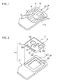
- a SIM card 10 as a first embodiment of the present invention includes an IC module 11 and a plate-like base member 12 to which the IC module 11 has been assembled.
- the IC module 11 includes a board 14, a circuit section 18 having a plurality of electronic components 16 mounted on a mounting surface 14A of the board 14, and an antenna 20 connected to the circuit section 18.
- the base member 12 is formed in a plate shape.
- a recessed portion 22 which accommodates the circuit section 18 is provided in the base member 12.
- the recessed portion 22 has an adhesive recessed portion 23 for adhering a peripheral edge 14B of the mounting surface 14A of the board 14 and an accommodating recessed portion 24 which accommodates the circuit section 18.
- the IC module 11 is assembled to the base member 12 by putting the peripheral edge 14B on the adhesive recessed portion 23 and adhering the peripheral edge 14B to the adhesive recessed portion 23 by an adhesive. In this state, the circuit section 18 is housed within the accommodating recessed portion 24.
- the mounting surface 14A of the board 14 is a surface on which a radio IC or a microcomputer IC and peripheral circuit components (electronic components) 16 thereof are mounted.
- a radio IC or a microcomputer IC and peripheral circuit components (electronic components) 16 thereof are mounted on the board 14.
- terminals 17 of the plurality of electronic components 16 are exposed on an exposed surface 14C opposite the mounting surface 14A (see Fig. 1 ).
- the antenna 20 includes a first antenna 31 formed on the exposed surface 14C of the board 14 and connected to the circuit section 18 and a second antenna 32 connected to the first antenna 31 and having a portion separated in the thickness direction of the board 14.
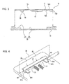
- the first antenna 31 has a pair of first terminals 31A (see Fig. 4 ) exposed from the mounting surface 14A.
- the second antenna 32 is a metal member having a pair of second terminals 32A respectively connected to the pair of first terminals 31A, a pair of leg portions 33 respectively raised from the pair of second terminals 32A, and a horizontal portion 3 4 provided over the pair of leg portions 33.
- the horizontal portion 34 is arranged to be substantially parallel to the mounting surface 14A, and has a three-dimensional structure arranged at a position shifted by a predetermined dimension H from the mounting surface 14A along the thickness direction of the board 14.
- the horizontal portion 34 is arranged at the position shifted from the mounting surface 14A by the predetermined dimension H, thereby forming the second antenna 32 in a substantial C shape by the pair of second terminals 32A, the pair of leg portions 33, and the horizontal portion 34. Accordingly, the pair of second terminals 32A are connected to the pair of first terminals 31A, thereby forming a loop antenna which circulates along a surface (a surface indicated by an imaginary line) 36 intersecting with the mounting surface 14A. Balanced feeding of radio-frequency signals from two ends of the loop antenna is made.
- a gain change of the antenna 20 can be suppressed to be small since it is possible to use the antenna 20 as the loop antenna by arranging the horizontal portion 34 to be substantially parallel to the mounting surface 14A using the antenna 20 as the loop antenna.
- An antenna gain change depending upon an arrangement state of the SIM card 10 is suppressed in the SIM card by suppressing a radio-frequency current from flowing outside an antenna section of the SIM card 10.
- An air core coil structure is formed by constituting the second antenna 32 by a metal member. Since a Q factor can be increased as the parasitic capacitance from a dielectric substance is decreased, the antenna gain can be improved. Miniaturization can be promoted since electronic components can be mounted just below the horizontal portion 34 by arranging the horizontal portion 34 at the position shifted from the mounting surface 14A by the predetermined dimension H.
- the loop antenna is constituted to have an axis (the horizontal portion 34) of a loop parallel to the mounting surface 14A as described above, the gain decrease is suppressed when the SIM card 10 is arranged in contact with a metal surface such as a battery.
- a radio-frequency signal flows through the entirety of the SIM card 10 when the SIM card 10 is arranged to be separated from the metal surface, and an increase in the antenna gain is suppressed.
- the antenna gain can be maintained to be substantially constant without depending upon an installation state of the SIM card 10.
- a SIM card 40 of the second embodiment shown in Figs. 5 and 6 is provided with a second antenna 41 in place of the second antenna 32 of the first embodiment, and a configuration thereof is the same as the SIM card 10 of the first embodiment.
- the second antenna 41 has an antenna board 42, a pair of through-holes 43 penetrating the antenna board 42 in the thickness direction, and a conductor portion (horizontal portion) 45 which connects the through-holes 43.
- the antenna board 42 is considered as a printed board, and is layered on a mounting surface 14A of a board 14, thereby forming the second antenna 41.
- the conductor portion 45 is arranged to be substantially parallel to the mounting surface 14A, and is arranged at a position shifted from the mounting surface 14A by a predetermined dimension H along the thickness direction of the board 14.
- the SIM card 40 of the second embodiment can have the same advantageous effect as the SIM card 10 of the first embodiment. According to the SIM card 40 of the second embodiment, it is possible to improve the yield and omit the adjustment since the high pattern accuracy is obtained by employing the conductor portion 45 of the printed board as the antenna board 42 as the second antenna 41.
- a SIM card 50 of the third embodiment shown in Figs. 7 and 8 is provided with an antenna 51 in place of the antenna 20 of the first embodiment, and a configuration thereof is the same as the SIM card 10 of the first embodiment.
- the antenna 51 has a first antenna 52 and a second antenna 53.
- the first antenna 52 is connected to a circuit portion 18 shown in Fig. 2 , and a pair of terminal portions 52A are exposed on an exposed surface (a surface of the IC module) 14C of a board 14.
- the second antenna 53 has a sheet-like printed board 55 on which a conductor 56 is printed.
- the printed board 55 of the second antenna 53 is folded to return from a front side 12A in which a recessed portion 22 (see Fig. 2 ) of a base member 12 is provided to the front side 12A via a backside 12B in which no recessed portion 22 is provided.
- two end portions 56A of the conductor 56 of the second antenna 53 are connected to the terminal portions 52A of the first antenna 52.
- a horizontal portion 56B of the conductor 56 is arranged to be parallel to the mounting surface 14A (see Fig. 2 ), and is arranged at a position shifted from the mounting surface 14A by a predetermined dimension H along the thickness direction of the board 14.
- the antenna 51 is the loop antenna formed by the first antenna 52 and the second antenna 53.
- the SIM card 50 of the third embodiment can have the same advantageous effect as the SIM card 10 of the first embodiment. According to the SIM card 50 of the third embodiment, it is possible to arrange the second antenna 53 outside the base member 12. It is possible to increase the degree of freedom in designing the IC module 11 or the base member 12. It is possible to increase a loop area and improve an antenna gain.
- a SIM card 60 of the fourth embodiment shown in Fig. 9 is provided with an antenna 61 in place of the antenna 20 of the first embodiment, and a configuration thereof is the same as the SIM card 10 of the first embodiment.
- the antenna 61 has a pair of terminal portions 62 connected to a circuit section 18 and exposed on a mounting surface (a surface of an IC module 11) 14A, a pair of contact portions 63 respectively connected to the pair of terminal portions 62, and a loop antenna 64 connected to the pair of contact portions 63.
- the pair of contact portions 63 are terminals embedded into the base member 12 and exposed on a recessed portion 22.
- the loop antenna 64 has a horizontal portion 65 which is embedded into the base member 12, arranged to be parallel to the mounting surface 14A, and arranged at a position shifted from the mounting surface 14A by a predetermined dimension H along the thickness direction of a board 14.
- the pair of terminal portions 62 are respectively in contact with the pair of contact portions 63.
- the loop antenna 64 is connected to the circuit section 18.
- the SIM card 60 of the fourth embodiment can have the same advantageous effect as the SIM card 10 of the first embodiment. According to the SIM card 60 of the fourth embodiment, it is possible to increase the degree of freedom in designing the IC module 11 by embedding the loop antenna 64 into the base member 12 outside the IC module 11.
- a SIM card 70 of the fifth embodiment shown in Fig. 10 is provided with an antenna 71 in place of the antenna 20 of the first embodiment, and a configuration thereof is the same as the SIM card 10 of the first embodiment.
- the antenna 71 has a first conductor 72 formed along a board 14 and a second conductor (conductor) 73 connected to the first conductor 72.
- the first conductor 72 has a pair of terminal portions 74 connected to a circuit section 18 and exposed on a mounting surface (a surface of an IC module 11) 14A.
- the second conductor 73 constitutes an antenna to be formed along a recessed portion 22, and two end portions 75 are exposed on an adhesive recessed portion 23.
- the second conductor 73 has a horizontal portion 77 arranged to be parallel to the mounting surface 14A and arranged at a position shifted from the mounting surface 14A by a predetermined dimension H along the thickness direction of the board 14.
- the pair of terminal portions 74 are respectively in contact with the two end portions 75.
- a loop antenna is formed by the first conductor 72 and the second conductor 73.
- the SIM card 70 of the fifth embodiment can have the same advantageous effect as the SIM card 10 of the first embodiment. According to the SIM card 70 of the fifth embodiment, it is possible to increase the degree of freedom in designing the IC module 11 by forming the second conductor 73 as the antenna along the recessed portion 22 outside the IC module 11.
- the SIM card 70 of the fifth embodiment it is possible to improve the yield and omit the adjustment since the high pattern accuracy is obtained by forming the antenna 71 by the first conductor 72 and the second conductor 73.
- a printed board may be unnecessary by providing the second conductor 73 along the recessed portion 22, and the simplification of configuration can be promoted.
- a SIM card 80 of the sixth embodiment shown in Figs. 11 and 12 is provided with an antenna 81 in place of the antenna 20 of the first embodiment, and a configuration thereof is the same as the SIM card 10 of the first embodiment.
- the antenna 81 has a first antenna 82 formed around the surface of a base member 12 and a second antenna 83 formed around the surface of a board 14.
- the first antenna 82 has a plurality of through-holes 84 penetrating the base member 12 in the thickness direction and a first conductor 85 which connects the pair of through-holes 84.
- the first antenna 82 is covered with a cover seal 80A.
- a through-hole (or recessed portion) 22 is formed and a plurality of through-holes 84 is exposed on a surface 86 facing the board 14.
- the first conductor 85 is arranged to be parallel to a mounting surface 14A and is arranged at a position shifted from the board 14 by a predetermined dimension H along the thickness direction of the board 14.
- the second antenna 83 has a plurality of terminal portions 87 embedded into the board 14 and exposed on the mounting surface 14A.
- the terminal portions 87 are respectively in contact with the through-holes 84.
- a loop antenna is formed by the first antenna 82 and the second antenna 83.
- the number of turns of the loop antenna may be 1, 2, 4, or more.
- the SIM card 80 of the sixth embodiment can have the same advantageous effect as the SIM card 10 of the first embodiment. According to the SIM card 80 of the sixth embodiment, it is possible to increase the degree of freedom in designing the IC module 11 by providing the first antenna 82 on the base member 12 outside the IC module 11.
- a SIM card 90 of the seventh embodiment shown in Fig. 13 (A) is constituted by providing external antenna terminals 91 and 92 connectable to an external antenna (not shown) on the SIM card 10 of the first embodiment, and a configuration thereof is the same as that of the SIM card 10 of the first embodiment.
- the external antenna terminals 91 and 92 are provided on a surface 12A of a base member 12.
- the external antenna (not shown) is arranged around the surface of a cellular phone, and has a larger structure than the SIM card 80, thereby securing a great communication distance.
- the communication distance can be further extended by separating the loop antenna built in the SIM card 90.
- the separation is not made, a transmission output signal is divided into two of the external antenna of the cellular phone and the built-in antenna, so that the communication distance becomes 1/ ⁇ 2, but the simplification of configuration can be promoted.
- a SIM card 95 of the modified example of the seventh embodiment shown in Fig. 13(B) is provided with external antenna terminals 96 and 97 for which balanced feeding is possible in place of the external antenna terminals 91 and 92 of the SIM card 90 of the seventh embodiment.
- the balanced feeding is possible. An antenna gain change can be suppressed, and a DC cut can be formed. Further, it is not necessary to adjust a DC level with the external antenna.
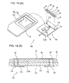
- a SIM card 100 of the eighth embodiment shown in Fig. 14(A) is a modified example of the above-described second embodiment, and has a pair of board through-holes 115 and 115 penetrating a board 114 of an IC module 101 in the thickness direction.
- the through-holes 115 and 115 are connected to a circuit section 18 of a mounting surface 114A via a wiring 116 which is conductible to a through-hole 43 of an antenna board 42 and is provided on the backside of the board 114.
- the eighth embodiment has an advantageous effect of improving an antenna gain since the loop height of the second antenna 41 as the loop antenna can be greatly secured by the through-holes 43 of the antenna board 42 and the board through-holes 115 and 115.
- the shapes of elements such as the IC module 11, and the base member 12, the board 14, the antennas 20, 51, 61, 71, and 81 or the recessed portion 22 illustrated in the above-described embodiments may be appropriately changed.
- the present invention has an IC module in which an antenna is connected to a circuit section on which an electronic component is mounted, and may preferably be applicable to a SIM card in which the IC module is accommodated.
Landscapes
- Engineering & Computer Science (AREA)
- Computer Hardware Design (AREA)
- Computer Networks & Wireless Communication (AREA)
- Microelectronics & Electronic Packaging (AREA)
- Physics & Mathematics (AREA)
- General Physics & Mathematics (AREA)
- Theoretical Computer Science (AREA)
- General Engineering & Computer Science (AREA)
- Support Of Aerials (AREA)
- Details Of Aerials (AREA)
- Credit Cards Or The Like (AREA)
Applications Claiming Priority (2)
| Application Number | Priority Date | Filing Date | Title |
|---|---|---|---|
| JP2007232982 | 2007-09-07 | ||
| PCT/JP2008/002465 WO2009031323A1 (fr) | 2007-09-07 | 2008-09-05 | Module à ci de carte sim et carte sim |
Publications (4)
| Publication Number | Publication Date |
|---|---|
| EP2202844A1 true EP2202844A1 (fr) | 2010-06-30 |
| EP2202844A4 EP2202844A4 (fr) | 2013-07-10 |
| EP2202844B1 EP2202844B1 (fr) | 2016-02-24 |
| EP2202844B8 EP2202844B8 (fr) | 2016-09-07 |
Family
ID=40428648
Family Applications (1)
| Application Number | Title | Priority Date | Filing Date |
|---|---|---|---|
| EP08829392.3A Not-in-force EP2202844B8 (fr) | 2007-09-07 | 2008-09-05 | Module à ci de carte sim et carte sim |
Country Status (6)
| Country | Link |
|---|---|
| US (1) | US7922097B2 (fr) |
| EP (1) | EP2202844B8 (fr) |
| JP (1) | JP4697817B2 (fr) |
| KR (1) | KR20100054822A (fr) |
| CN (2) | CN101584081B (fr) |
| WO (1) | WO2009031323A1 (fr) |
Cited By (3)
| Publication number | Priority date | Publication date | Assignee | Title |
|---|---|---|---|---|
| EP2472669A1 (fr) * | 2010-12-29 | 2012-07-04 | Samsung Electro-Mechanics Co., Ltd | Carte SIM avec antenne, assemblage, son procédé de fabrication et dispositif électronique l'incluant |
| EP2570973A1 (fr) * | 2011-09-16 | 2013-03-20 | Gemalto SA | Procédé d'établissement d'une communication sans fil et carte à puce associée |
| US9203834B2 (en) | 2013-03-14 | 2015-12-01 | Samsung Electronics Co., Ltd. | Computing system with identification mechanism and method of operation thereof |
Families Citing this family (23)
| Publication number | Priority date | Publication date | Assignee | Title |
|---|---|---|---|---|
| US8544755B2 (en) * | 2010-06-28 | 2013-10-01 | United Test And Assembly Center Ltd. | Subscriber identity module (SIM) card |
| CN103117447A (zh) * | 2011-10-25 | 2013-05-22 | 安泰科技有限公司 | 便携式终端以及形成有天线的sim卡连接器 |
| US8649820B2 (en) | 2011-11-07 | 2014-02-11 | Blackberry Limited | Universal integrated circuit card apparatus and related methods |
| CN102411720A (zh) * | 2011-11-12 | 2012-04-11 | 成都雷电微力科技有限公司 | Rfid天线系统 |
| USD720354S1 (en) * | 2011-11-22 | 2014-12-30 | Kabushiki Kaisha Toshiba | Module with built-in integrated circuits for use with IC card |
| US8936199B2 (en) | 2012-04-13 | 2015-01-20 | Blackberry Limited | UICC apparatus and related methods |
| USD703208S1 (en) * | 2012-04-13 | 2014-04-22 | Blackberry Limited | UICC apparatus |
| USD701864S1 (en) * | 2012-04-23 | 2014-04-01 | Blackberry Limited | UICC apparatus |
| USD707682S1 (en) * | 2012-12-05 | 2014-06-24 | Logomotion, S.R.O. | Memory card |
| US9165237B2 (en) * | 2012-12-19 | 2015-10-20 | Stmicroelectronics S.R.L. | SIM card adapter |
| US9888283B2 (en) | 2013-03-13 | 2018-02-06 | Nagrastar Llc | Systems and methods for performing transport I/O |
| US9647997B2 (en) | 2013-03-13 | 2017-05-09 | Nagrastar, Llc | USB interface for performing transport I/O |
| USD758372S1 (en) * | 2013-03-13 | 2016-06-07 | Nagrastar Llc | Smart card interface |
| USD729808S1 (en) | 2013-03-13 | 2015-05-19 | Nagrastar Llc | Smart card interface |
| USD759022S1 (en) * | 2013-03-13 | 2016-06-14 | Nagrastar Llc | Smart card interface |
| KR102069034B1 (ko) * | 2013-07-15 | 2020-01-22 | 에스케이 텔레콤주식회사 | 안테나 단자를 포함하는 정보저장 장치 |
| DE102014106815B4 (de) * | 2014-05-14 | 2024-01-18 | Infineon Technologies Ag | Kommunikationsmodul |
| USD780763S1 (en) | 2015-03-20 | 2017-03-07 | Nagrastar Llc | Smart card interface |
| USD864968S1 (en) | 2015-04-30 | 2019-10-29 | Echostar Technologies L.L.C. | Smart card interface |
| USD798868S1 (en) * | 2015-08-20 | 2017-10-03 | Isaac S. Daniel | Combined subscriber identification module and storage card |
| CN105160384B (zh) * | 2015-09-28 | 2017-12-22 | 北京世纪光信科技有限公司 | 一种贴膜卡的卡基 |
| US9900984B2 (en) * | 2015-12-31 | 2018-02-20 | Taisys Technologies Co. Ltd. | Auxiliary mounting structure for mounting advanced smart card |
| KR102531501B1 (ko) * | 2020-11-27 | 2023-05-11 | 주식회사 씨앤엠 | 생체 인식 스마트카드 및 그 제조 방법 |
Family Cites Families (30)
| Publication number | Priority date | Publication date | Assignee | Title |
|---|---|---|---|---|
| JPS6323404A (ja) | 1986-07-16 | 1988-01-30 | Mitsubishi Electric Corp | マイクロストリツプアンテナ |
| JPH02220505A (ja) | 1989-02-22 | 1990-09-03 | Hitachi Ltd | マイクロ波アンテナ |
| JP2870940B2 (ja) | 1990-03-01 | 1999-03-17 | 株式会社豊田中央研究所 | 車載アンテナ |
| JPH0467805A (ja) | 1990-07-10 | 1992-03-03 | Jmk Intern Inc | マイクロウェーブ作動ヘアーカーラー |
| JPH07115313A (ja) * | 1992-10-09 | 1995-05-02 | Asahi Glass Co Ltd | 自動車用の高周波ガラスアンテナ |
| US5568156A (en) * | 1992-10-09 | 1996-10-22 | Asahi Glass Company Ltd. | High frequency wave glass antenna for an automobile |
| JP3737606B2 (ja) | 1997-06-30 | 2006-01-18 | 株式会社日立国際電気 | 平面アンテナ |
| JPH11205424A (ja) * | 1998-01-09 | 1999-07-30 | Denso Corp | 無線通信装置 |
| DE19922699C2 (de) | 1999-05-18 | 2001-05-17 | Hirschmann Electronics Gmbh | Antenne mit wenigstens einem Vertikalstrahler |
| EP1056222A1 (fr) * | 1999-05-24 | 2000-11-29 | ICO Services Ltd. | Multiplexage de données pour fonctionnement en diversité |
| JP2001326514A (ja) | 2000-05-18 | 2001-11-22 | Sharp Corp | 携帯無線機用アンテナ |
| JP2001344583A (ja) * | 2000-06-01 | 2001-12-14 | Dainippon Printing Co Ltd | Icキャリア |
| US6634564B2 (en) * | 2000-10-24 | 2003-10-21 | Dai Nippon Printing Co., Ltd. | Contact/noncontact type data carrier module |
| JP2002203224A (ja) * | 2000-10-24 | 2002-07-19 | Dainippon Printing Co Ltd | 接触式および非接触式兼用のデータキャリアモジュール |
| JP2002236901A (ja) * | 2001-02-08 | 2002-08-23 | Dainippon Printing Co Ltd | 電子情報記録媒体、および、電子情報読み取り・書込み装置 |
| JP4109029B2 (ja) | 2002-07-19 | 2008-06-25 | 大日本印刷株式会社 | Icカード代替機能を有する携帯機器 |
| DE60326598D1 (de) * | 2002-08-26 | 2009-04-23 | Dainippon Printing Co Ltd | Sim, ic-modul und ic-karte |
| JP4240990B2 (ja) | 2002-10-16 | 2009-03-18 | 大日本印刷株式会社 | Icモジュール回路基板 |
| CA2506931A1 (fr) * | 2002-12-20 | 2004-07-08 | Nagracard Sa | Dispositif de securisation pour connecteur de module de securite |
| EP1600885B1 (fr) * | 2003-02-25 | 2010-02-10 | Dai Nippon Printing Co., Ltd. | Lecteur-editeur de carte sim |
| JP2005204188A (ja) * | 2004-01-19 | 2005-07-28 | Dainippon Printing Co Ltd | 携帯可能な非接触通信デバイス |
| JP2005157927A (ja) * | 2003-11-28 | 2005-06-16 | Dainippon Printing Co Ltd | 液晶ディスプレイ付きuimリーダライタ |
| JP2004295480A (ja) * | 2003-03-27 | 2004-10-21 | Jr East Mechatronics Co Ltd | 非接触icモジュール |
| JP4422494B2 (ja) * | 2003-05-07 | 2010-02-24 | 大日本印刷株式会社 | Icカードおよびsim |
| JP2005005866A (ja) * | 2003-06-10 | 2005-01-06 | Alps Electric Co Ltd | アンテナ一体型モジュール |
| JP2005234838A (ja) | 2004-02-19 | 2005-09-02 | Dainippon Printing Co Ltd | Uimアダプタ |
| HK1063994A2 (en) * | 2004-06-09 | 2004-12-17 | 龙杰智能卡有限公司 | Smart card reader with contactless access capability |
| JP4676734B2 (ja) | 2004-09-15 | 2011-04-27 | 大日本印刷株式会社 | Simリーダライタ |
| CN100362887C (zh) * | 2005-10-24 | 2008-01-16 | 莫宁 | 内置射频识别读写器的手机 |
| JP2008210301A (ja) * | 2007-02-28 | 2008-09-11 | Sony Corp | 記憶媒体、通信システム、並びに制御装置。 |
-
2008
- 2008-09-05 EP EP08829392.3A patent/EP2202844B8/fr not_active Not-in-force
- 2008-09-05 CN CN2008800025711A patent/CN101584081B/zh not_active Expired - Fee Related
- 2008-09-05 WO PCT/JP2008/002465 patent/WO2009031323A1/fr not_active Ceased
- 2008-09-05 JP JP2008556340A patent/JP4697817B2/ja not_active Expired - Fee Related
- 2008-09-05 KR KR1020107005058A patent/KR20100054822A/ko not_active Withdrawn
- 2008-09-05 US US12/677,015 patent/US7922097B2/en active Active
- 2008-09-08 CN CNU2008201300592U patent/CN201281865Y/zh not_active Expired - Fee Related
Cited By (4)
| Publication number | Priority date | Publication date | Assignee | Title |
|---|---|---|---|---|
| EP2472669A1 (fr) * | 2010-12-29 | 2012-07-04 | Samsung Electro-Mechanics Co., Ltd | Carte SIM avec antenne, assemblage, son procédé de fabrication et dispositif électronique l'incluant |
| EP2570973A1 (fr) * | 2011-09-16 | 2013-03-20 | Gemalto SA | Procédé d'établissement d'une communication sans fil et carte à puce associée |
| WO2013037600A1 (fr) * | 2011-09-16 | 2013-03-21 | Gemalto S.A. | Procédé d'établissement de communication sans fil et carte à puce associée |
| US9203834B2 (en) | 2013-03-14 | 2015-12-01 | Samsung Electronics Co., Ltd. | Computing system with identification mechanism and method of operation thereof |
Also Published As
| Publication number | Publication date |
|---|---|
| CN101584081B (zh) | 2013-02-27 |
| EP2202844B8 (fr) | 2016-09-07 |
| US20100176207A1 (en) | 2010-07-15 |
| CN101584081A (zh) | 2009-11-18 |
| US7922097B2 (en) | 2011-04-12 |
| EP2202844B1 (fr) | 2016-02-24 |
| WO2009031323A1 (fr) | 2009-03-12 |
| JPWO2009031323A1 (ja) | 2010-12-09 |
| JP4697817B2 (ja) | 2011-06-08 |
| CN201281865Y (zh) | 2009-07-29 |
| KR20100054822A (ko) | 2010-05-25 |
| EP2202844A4 (fr) | 2013-07-10 |
Similar Documents
| Publication | Publication Date | Title |
|---|---|---|
| EP2202844A1 (fr) | Module à ci de carte sim et carte sim | |
| EP2811656B1 (fr) | Dispositif d'antenne et dispositif de communication sans fil | |
| KR101044994B1 (ko) | 휴대 단말기의 안테나 장치 | |
| CN207852935U (zh) | 天线装置以及电子设备 | |
| US8090407B2 (en) | Contactless smart SIM | |
| US8692728B2 (en) | Method for an antenna ground plane extension | |
| US10917137B2 (en) | NFC antenna in a mobile device | |
| US9099774B2 (en) | Antenna | |
| JP5720807B2 (ja) | アンテナ装置および通信端末装置 | |
| JP5472455B2 (ja) | 通信端末およびカード型アンテナモジュール | |
| GB2525869A (en) | Smart card module | |
| CN106450661B (zh) | 天线装置、电子设备以及天线装置的安装方法 | |
| GB2537773A (en) | Antenna apparatus and communication terminal instrument | |
| US8581787B2 (en) | Portable electronic device with antenna module | |
| US10122065B2 (en) | Antenna device, card information medium, electronic apparatus, and method for manufacturing antenna device | |
| JP2012090251A (ja) | アンテナ装置 | |
| CN207517887U (zh) | 天线装置以及rfid系统 | |
| CN207910065U (zh) | 天线装置及电子设备 | |
| US8939378B2 (en) | Smartcard connector with RFID module | |
| KR101321874B1 (ko) | Nfc 소형화 안테나 및 이를 이용한 rfid 태그 | |
| US20090303151A1 (en) | Low profile gps antenna assembly | |
| CN207149699U (zh) | 天线装置以及电子设备 |
Legal Events
| Date | Code | Title | Description |
|---|---|---|---|
| PUAI | Public reference made under article 153(3) epc to a published international application that has entered the european phase |
Free format text: ORIGINAL CODE: 0009012 |
|
| 17P | Request for examination filed |
Effective date: 20100407 |
|
| AK | Designated contracting states |
Kind code of ref document: A1 Designated state(s): AT BE BG CH CY CZ DE DK EE ES FI FR GB GR HR HU IE IS IT LI LT LU LV MC MT NL NO PL PT RO SE SI SK TR |
|
| AX | Request for extension of the european patent |
Extension state: AL BA MK RS |
|
| DAX | Request for extension of the european patent (deleted) | ||
| A4 | Supplementary search report drawn up and despatched |
Effective date: 20130612 |
|
| RIC1 | Information provided on ipc code assigned before grant |
Ipc: G06K 19/07 20060101ALI20130606BHEP Ipc: H01Q 1/24 20060101ALN20130606BHEP Ipc: H01Q 1/38 20060101AFI20130606BHEP Ipc: H01Q 1/22 20060101ALN20130606BHEP Ipc: H01Q 7/00 20060101ALI20130606BHEP Ipc: G06K 19/077 20060101ALI20130606BHEP |
|
| 17Q | First examination report despatched |
Effective date: 20140311 |
|
| GRAP | Despatch of communication of intention to grant a patent |
Free format text: ORIGINAL CODE: EPIDOSNIGR1 |
|
| RIC1 | Information provided on ipc code assigned before grant |
Ipc: G06K 19/07 20060101ALI20150807BHEP Ipc: G06K 19/077 20060101ALI20150807BHEP Ipc: H01Q 1/22 20060101ALN20150807BHEP Ipc: H01Q 1/24 20060101ALN20150807BHEP Ipc: H01Q 1/38 20060101AFI20150807BHEP Ipc: H01Q 7/00 20060101ALI20150807BHEP |
|
| INTG | Intention to grant announced |
Effective date: 20150831 |
|
| GRAS | Grant fee paid |
Free format text: ORIGINAL CODE: EPIDOSNIGR3 |
|
| GRAA | (expected) grant |
Free format text: ORIGINAL CODE: 0009210 |
|
| AK | Designated contracting states |
Kind code of ref document: B1 Designated state(s): AT BE BG CH CY CZ DE DK EE ES FI FR GB GR HR HU IE IS IT LI LT LU LV MC MT NL NO PL PT RO SE SI SK TR |
|
| REG | Reference to a national code |
Ref country code: GB Ref legal event code: FG4D |
|
| REG | Reference to a national code |
Ref country code: CH Ref legal event code: EP |
|
| REG | Reference to a national code |
Ref country code: AT Ref legal event code: REF Ref document number: 777162 Country of ref document: AT Kind code of ref document: T Effective date: 20160315 |
|
| REG | Reference to a national code |
Ref country code: IE Ref legal event code: FG4D |
|
| REG | Reference to a national code |
Ref country code: DE Ref legal event code: R096 Ref document number: 602008042531 Country of ref document: DE |
|
| REG | Reference to a national code |
Ref country code: LT Ref legal event code: MG4D |
|
| GRAM | Information related to correction after decision after decision to grant or to maintain patent in amended form deleted |
Free format text: ORIGINAL CODE: EPIDOSDCDEC |
|
| GRAT | Correction requested after decision to grant or after decision to maintain patent in amended form |
Free format text: ORIGINAL CODE: EPIDOSNCDEC |
|
| REG | Reference to a national code |
Ref country code: NL Ref legal event code: MP Effective date: 20160224 |
|
| REG | Reference to a national code |
Ref country code: AT Ref legal event code: MK05 Ref document number: 777162 Country of ref document: AT Kind code of ref document: T Effective date: 20160224 |
|
| RIN2 | Information on inventor provided after grant (corrected) |
Inventor name: MIYASHITA, NORIHIRO Inventor name: YOSHIKAWA, YOSHISHIGE |
|
| PG25 | Lapsed in a contracting state [announced via postgrant information from national office to epo] |
Ref country code: FI Free format text: LAPSE BECAUSE OF FAILURE TO SUBMIT A TRANSLATION OF THE DESCRIPTION OR TO PAY THE FEE WITHIN THE PRESCRIBED TIME-LIMIT Effective date: 20160224 Ref country code: ES Free format text: LAPSE BECAUSE OF FAILURE TO SUBMIT A TRANSLATION OF THE DESCRIPTION OR TO PAY THE FEE WITHIN THE PRESCRIBED TIME-LIMIT Effective date: 20160224 Ref country code: HR Free format text: LAPSE BECAUSE OF FAILURE TO SUBMIT A TRANSLATION OF THE DESCRIPTION OR TO PAY THE FEE WITHIN THE PRESCRIBED TIME-LIMIT Effective date: 20160224 Ref country code: NO Free format text: LAPSE BECAUSE OF FAILURE TO SUBMIT A TRANSLATION OF THE DESCRIPTION OR TO PAY THE FEE WITHIN THE PRESCRIBED TIME-LIMIT Effective date: 20160524 Ref country code: IT Free format text: LAPSE BECAUSE OF FAILURE TO SUBMIT A TRANSLATION OF THE DESCRIPTION OR TO PAY THE FEE WITHIN THE PRESCRIBED TIME-LIMIT Effective date: 20160224 |
|
| PG25 | Lapsed in a contracting state [announced via postgrant information from national office to epo] |
Ref country code: LV Free format text: LAPSE BECAUSE OF FAILURE TO SUBMIT A TRANSLATION OF THE DESCRIPTION OR TO PAY THE FEE WITHIN THE PRESCRIBED TIME-LIMIT Effective date: 20160224 Ref country code: PL Free format text: LAPSE BECAUSE OF FAILURE TO SUBMIT A TRANSLATION OF THE DESCRIPTION OR TO PAY THE FEE WITHIN THE PRESCRIBED TIME-LIMIT Effective date: 20160224 Ref country code: PT Free format text: LAPSE BECAUSE OF FAILURE TO SUBMIT A TRANSLATION OF THE DESCRIPTION OR TO PAY THE FEE WITHIN THE PRESCRIBED TIME-LIMIT Effective date: 20160624 Ref country code: LT Free format text: LAPSE BECAUSE OF FAILURE TO SUBMIT A TRANSLATION OF THE DESCRIPTION OR TO PAY THE FEE WITHIN THE PRESCRIBED TIME-LIMIT Effective date: 20160224 Ref country code: NL Free format text: LAPSE BECAUSE OF FAILURE TO SUBMIT A TRANSLATION OF THE DESCRIPTION OR TO PAY THE FEE WITHIN THE PRESCRIBED TIME-LIMIT Effective date: 20160224 Ref country code: AT Free format text: LAPSE BECAUSE OF FAILURE TO SUBMIT A TRANSLATION OF THE DESCRIPTION OR TO PAY THE FEE WITHIN THE PRESCRIBED TIME-LIMIT Effective date: 20160224 Ref country code: SE Free format text: LAPSE BECAUSE OF FAILURE TO SUBMIT A TRANSLATION OF THE DESCRIPTION OR TO PAY THE FEE WITHIN THE PRESCRIBED TIME-LIMIT Effective date: 20160224 |
|
| PG25 | Lapsed in a contracting state [announced via postgrant information from national office to epo] |
Ref country code: DK Free format text: LAPSE BECAUSE OF FAILURE TO SUBMIT A TRANSLATION OF THE DESCRIPTION OR TO PAY THE FEE WITHIN THE PRESCRIBED TIME-LIMIT Effective date: 20160224 Ref country code: EE Free format text: LAPSE BECAUSE OF FAILURE TO SUBMIT A TRANSLATION OF THE DESCRIPTION OR TO PAY THE FEE WITHIN THE PRESCRIBED TIME-LIMIT Effective date: 20160224 |
|
| REG | Reference to a national code |
Ref country code: DE Ref legal event code: R097 Ref document number: 602008042531 Country of ref document: DE |
|
| PG25 | Lapsed in a contracting state [announced via postgrant information from national office to epo] |
Ref country code: RO Free format text: LAPSE BECAUSE OF FAILURE TO SUBMIT A TRANSLATION OF THE DESCRIPTION OR TO PAY THE FEE WITHIN THE PRESCRIBED TIME-LIMIT Effective date: 20160224 Ref country code: CZ Free format text: LAPSE BECAUSE OF FAILURE TO SUBMIT A TRANSLATION OF THE DESCRIPTION OR TO PAY THE FEE WITHIN THE PRESCRIBED TIME-LIMIT Effective date: 20160224 Ref country code: SK Free format text: LAPSE BECAUSE OF FAILURE TO SUBMIT A TRANSLATION OF THE DESCRIPTION OR TO PAY THE FEE WITHIN THE PRESCRIBED TIME-LIMIT Effective date: 20160224 |
|
| PG25 | Lapsed in a contracting state [announced via postgrant information from national office to epo] |
Ref country code: BE Free format text: LAPSE BECAUSE OF FAILURE TO SUBMIT A TRANSLATION OF THE DESCRIPTION OR TO PAY THE FEE WITHIN THE PRESCRIBED TIME-LIMIT Effective date: 20160224 |
|
| PLBE | No opposition filed within time limit |
Free format text: ORIGINAL CODE: 0009261 |
|
| STAA | Information on the status of an ep patent application or granted ep patent |
Free format text: STATUS: NO OPPOSITION FILED WITHIN TIME LIMIT |
|
| 26N | No opposition filed |
Effective date: 20161125 |
|
| PG25 | Lapsed in a contracting state [announced via postgrant information from national office to epo] |
Ref country code: BG Free format text: LAPSE BECAUSE OF FAILURE TO SUBMIT A TRANSLATION OF THE DESCRIPTION OR TO PAY THE FEE WITHIN THE PRESCRIBED TIME-LIMIT Effective date: 20160524 Ref country code: SI Free format text: LAPSE BECAUSE OF FAILURE TO SUBMIT A TRANSLATION OF THE DESCRIPTION OR TO PAY THE FEE WITHIN THE PRESCRIBED TIME-LIMIT Effective date: 20160224 |
|
| PG25 | Lapsed in a contracting state [announced via postgrant information from national office to epo] |
Ref country code: MC Free format text: LAPSE BECAUSE OF FAILURE TO SUBMIT A TRANSLATION OF THE DESCRIPTION OR TO PAY THE FEE WITHIN THE PRESCRIBED TIME-LIMIT Effective date: 20160224 |
|
| REG | Reference to a national code |
Ref country code: CH Ref legal event code: PL |
|
| GBPC | Gb: european patent ceased through non-payment of renewal fee |
Effective date: 20160905 |
|
| REG | Reference to a national code |
Ref country code: IE Ref legal event code: MM4A |
|
| REG | Reference to a national code |
Ref country code: FR Ref legal event code: ST Effective date: 20170531 |
|
| PG25 | Lapsed in a contracting state [announced via postgrant information from national office to epo] |
Ref country code: LI Free format text: LAPSE BECAUSE OF NON-PAYMENT OF DUE FEES Effective date: 20160930 Ref country code: FR Free format text: LAPSE BECAUSE OF NON-PAYMENT OF DUE FEES Effective date: 20160930 Ref country code: CH Free format text: LAPSE BECAUSE OF NON-PAYMENT OF DUE FEES Effective date: 20160930 Ref country code: IE Free format text: LAPSE BECAUSE OF NON-PAYMENT OF DUE FEES Effective date: 20160905 Ref country code: GB Free format text: LAPSE BECAUSE OF NON-PAYMENT OF DUE FEES Effective date: 20160905 |
|
| PG25 | Lapsed in a contracting state [announced via postgrant information from national office to epo] |
Ref country code: LU Free format text: LAPSE BECAUSE OF NON-PAYMENT OF DUE FEES Effective date: 20160905 |
|
| PG25 | Lapsed in a contracting state [announced via postgrant information from national office to epo] |
Ref country code: HU Free format text: LAPSE BECAUSE OF FAILURE TO SUBMIT A TRANSLATION OF THE DESCRIPTION OR TO PAY THE FEE WITHIN THE PRESCRIBED TIME-LIMIT; INVALID AB INITIO Effective date: 20080905 Ref country code: CY Free format text: LAPSE BECAUSE OF FAILURE TO SUBMIT A TRANSLATION OF THE DESCRIPTION OR TO PAY THE FEE WITHIN THE PRESCRIBED TIME-LIMIT Effective date: 20160224 |
|
| PG25 | Lapsed in a contracting state [announced via postgrant information from national office to epo] |
Ref country code: MT Free format text: LAPSE BECAUSE OF NON-PAYMENT OF DUE FEES Effective date: 20160930 Ref country code: TR Free format text: LAPSE BECAUSE OF FAILURE TO SUBMIT A TRANSLATION OF THE DESCRIPTION OR TO PAY THE FEE WITHIN THE PRESCRIBED TIME-LIMIT Effective date: 20160224 Ref country code: IS Free format text: LAPSE BECAUSE OF FAILURE TO SUBMIT A TRANSLATION OF THE DESCRIPTION OR TO PAY THE FEE WITHIN THE PRESCRIBED TIME-LIMIT Effective date: 20160224 Ref country code: GR Free format text: LAPSE BECAUSE OF FAILURE TO SUBMIT A TRANSLATION OF THE DESCRIPTION OR TO PAY THE FEE WITHIN THE PRESCRIBED TIME-LIMIT Effective date: 20160224 |
|
| PGFP | Annual fee paid to national office [announced via postgrant information from national office to epo] |
Ref country code: DE Payment date: 20220609 Year of fee payment: 15 |
|
| REG | Reference to a national code |
Ref country code: DE Ref legal event code: R119 Ref document number: 602008042531 Country of ref document: DE |
|
| PG25 | Lapsed in a contracting state [announced via postgrant information from national office to epo] |
Ref country code: DE Free format text: LAPSE BECAUSE OF NON-PAYMENT OF DUE FEES Effective date: 20240403 |