EP2203902B1 - Détecteur de pièces de monnaie - Google Patents
Détecteur de pièces de monnaie Download PDFInfo
- Publication number
- EP2203902B1 EP2203902B1 EP08841778A EP08841778A EP2203902B1 EP 2203902 B1 EP2203902 B1 EP 2203902B1 EP 08841778 A EP08841778 A EP 08841778A EP 08841778 A EP08841778 A EP 08841778A EP 2203902 B1 EP2203902 B1 EP 2203902B1
- Authority
- EP
- European Patent Office
- Prior art keywords
- coin
- sensor
- model
- drive
- signal
- Prior art date
- Legal status (The legal status is an assumption and is not a legal conclusion. Google has not performed a legal analysis and makes no representation as to the accuracy of the status listed.)
- Not-in-force
Links
Images



Classifications
-
- G—PHYSICS
- G07—CHECKING-DEVICES
- G07D—HANDLING OF COINS OR VALUABLE PAPERS, e.g. TESTING, SORTING BY DENOMINATIONS, COUNTING, DISPENSING, CHANGING OR DEPOSITING
- G07D5/00—Testing specially adapted to determine the identity or genuineness of coins, e.g. for segregating coins which are unacceptable or alien to a currency
- G07D5/08—Testing the magnetic or electric properties
-
- G—PHYSICS
- G01—MEASURING; TESTING
- G01B—MEASURING LENGTH, THICKNESS OR SIMILAR LINEAR DIMENSIONS; MEASURING ANGLES; MEASURING AREAS; MEASURING IRREGULARITIES OF SURFACES OR CONTOURS
- G01B7/00—Measuring arrangements characterised by the use of electric or magnetic techniques
- G01B7/02—Measuring arrangements characterised by the use of electric or magnetic techniques for measuring length, width or thickness
- G01B7/06—Measuring arrangements characterised by the use of electric or magnetic techniques for measuring length, width or thickness for measuring thickness
-
- G—PHYSICS
- G01—MEASURING; TESTING
- G01B—MEASURING LENGTH, THICKNESS OR SIMILAR LINEAR DIMENSIONS; MEASURING ANGLES; MEASURING AREAS; MEASURING IRREGULARITIES OF SURFACES OR CONTOURS
- G01B7/00—Measuring arrangements characterised by the use of electric or magnetic techniques
- G01B7/02—Measuring arrangements characterised by the use of electric or magnetic techniques for measuring length, width or thickness
- G01B7/06—Measuring arrangements characterised by the use of electric or magnetic techniques for measuring length, width or thickness for measuring thickness
- G01B7/10—Measuring arrangements characterised by the use of electric or magnetic techniques for measuring length, width or thickness for measuring thickness using magnetic means, e.g. by measuring change of reluctance
Definitions
- This invention relates to a coin sensor and to a method for determining the authenticity and/or denomination of a coin using a coin sensor.
- an inductance is mounted in proximity to a coin path so that the field generated by applying a drive signal to the inductance is influenced by the coin as it passes.
- US-A-4717006 discloses a number of time-domain eddy-current measurement arrangements.
- the disclosure indicates that it is possible to use, as the coin sensor, either a single coil or a pair of transmit/receive coils.
- the output voltage across the coil is measured after the drive voltage is switched off. The output voltage will decrease at a rate dependent upon the material structure of the coin.
- the coin passes in proximity to both coils, the drive signal is applied to the transmit coil, and the effects of the coin are determined by measuring the output of the receive coil.
- the disclosed arrangements are unsuitable for extracting detailed measurement information relating to coins with thin plating, such as plated steel coins.
- the measurement In order to perform measurements which are indicative of the very thin plating material, it is necessary to take samples very close to (soon before or after) a voltage transition in the drive signal.
- the measurement Preferably, the measurement should include measurements taken at around two, four and eight microseconds before or after a transition.
- the disclosed circuits would not be able to achieve accurate measurements at these timings. In the single coil arrangement, if the resistance across the inductance is low, it would take a significant amount of time to discharge the energy in the coil after a transition, resulting in "ringing", which would mask the effects of the decaying eddy currents in the coil.
- the document EP 1 172 772 A2 discloses a method and apparatus for obtaining physical characteristics of coins for their identification, which consists in submitting the coins to two consecutive stages of electromagnetic measurement, defined by a first and a second pairs of coils, in one of said pairs the coils are connected in such a manner that their magnetic fields are added and in the other in such a way that their magnetic fields are subtracted, which stages providing signals which are processed to obtain parameters representative of the coin, characterised in that the four coils are connected to each other according to a bridge configuration and in that they are supplied simultaneously with at least two, and preferably 3, signals of different frequencies, obtaining simultaneously in each stage, on passage of the coins, two full bridge signals for each frequency and a further two half-bridge signals for the highest frequency, in each case one of the signals being representative of the variation of the resistive component.
- the document US3,675,244 discloses a coin acceptor that detects the bulk resistivity and permeability of a coin and determines whether or not the coin is valid.
- a two-coil inductor forms one arm of a normally unbalanced Maxwell bridge and is disposed at a test station which is interposed in a channel through which the coin passes.
- the two coils have series aiding magnetic fields and are disposed on opposite sides of the coin channel with the lines of force crossing the channel at generally right angles to the opposed faces of a coin under test.
- a valid coin moving through the lines of force causes the inductance to change and effect balancing of the bridge. If this occurs throughout a predetermined test period, a coin deflector below the test station is withdrawn to permit the coin to enter an accept path.
- the new approach regards the relationship between the eddy current probe excitation and sensor response as a system, uses the system identification techniques to establish a transfer function model for the system from the excitation and response data, and extracts the features of inspected structures from the identified transfer function model parameters for non-destructive evaluations.
- the use of the new approach in experimental studies verifies its effectiveness and demonstrates its potential in engineering applications.
- the invention provides two separate solutions to the problems set out above, one relating to the hardware structure of a coin sensor for time-domain eddy-current measurements and the other relating to an improved method of processing such measurements, or different types of measurements, of a coin. Although these solutions can be used independently, there are particular advantages using them in combination.
- a coin sensor is arranged to perform time-domain eddy-current measurements using an inductance, wherein the inductance forms one arm of an AC bridge.
- An AC bridge divides the current generated by a drive signal into two paths, each comprising two arms connected in series, the output of the bridge being taken from the junction between the arms in the first path and the junction between the arms in the second path.
- the two paths When in balance, the two paths have matching AC characteristics and the output is zero.
- the AC characteristics of only one of the paths, containing the inductance are changed when a coin is close to the inductance.
- the bridge is substantially in balance when no coin is in proximity to the inductance.
- the output signal of the bridge changes from substantially zero to a value dependent upon the coin characteristics.
- This proportionately very large change facilitates the detection of the effects of small eddy-currents, while the impedance characteristics of the bridge prevent "ringing" of the inductance.
- the bridge is preferably a Maxwell bridge, with the AC characteristics in the path containing the inductance being matched by virtue of the presence of a capacitor in the other path.
- bridge circuits have been used in the past in coin sensors (e.g. in US-A-4513762 ) these have generally been operated with single-frequency drive signals and tuned so that the presence of coins of a specific denomination causes null values to appear across the bridge. Such arrangements would not be suitable for use with broadband signals as used in the present invention.
- coin testing is carried out by using a coin sensor to derive multiple measurements of a coin, and then deriving the coefficients of a model of the transfer function of the coin and the sensor.
- the coefficients can be derived using known mathematical techniques and algorithms, such as iterative or estimation techniques, using input and output samples and the model.
- the coefficients for a given model can be derived by adjusting the coefficients of the model so that it models the transfer function of the coin and the sensor, as indicated by the model output corresponding to the measurement samples.
- Acceptance criteria are then applied using the coefficients, for example, by applying acceptance criteria to the coefficients, or data derived from the coefficients, to determine the class or denomination of the coin.
- a drive signal which is used to drive the coin sensor is also applied to the model.
- the drive signal is complex and/or variable, and possibly random, and consequently the model can be made much simpler and more effective by excluding the drive signal itself, which instead is applied as an input to the model.
- the coin tester may have more than one sensor.
- Each sensor may have a respective model or models.
- a combination of sensors may be modelled together, for example, using a multiple input multiple output (MIMO) model.
- MIMO multiple input multiple output
- the measurements are preferably time-domain eddy-current measurements, and are preferably derived using a sensor according to the preceding aspect of the invention.
- the invention also provides an apparatus arranged to carry out the steps of the method, for example, using suitable hardware and/or software components, such as a processor.
- a coin tester 2 in accordance with the present invention is shown in Fig. 1 .
- the coin tester 2 comprises a coin sensor 4, a drive circuit 6 and a processing circuit 8.
- the coin sensor 4 has an input terminal 10 and a Maxwell bridge circuit 12 connected between the input terminal 10 and ground.
- the bridge circuit 12 has two paths between the input terminal 10 and ground.
- a first path comprises a first arm including R1 connected in series with a second arm comprising a capacitor C, the parasitic resistance of which is indicated at RC.
- the second path comprises a third arm including an inductance L connected in series with a fourth arm comprising a resistor R2.
- the inherent resistance of the coil L is indicated at RL.
- the output of the bridge 12 is derived from a first terminal A at the junction between resistor R1 and capacitor C in the first path, and a second terminal B between the conductor L and the resistor R2 in the second path.
- the signals at these points A and B are applied to a differential amplifier U1, whose output forms the output 14 of the coin sensor 4.
- T 2 L R 2 + R L .
- the inductance L is formed of a single coil in proximity to a coin path, and produces a field which is influenced by the presence of a coin 16 travelling along the coin path. (Although it would be possible to form the inductance L of more than one coil, the combined properties of the coils would represent a single inductance in the bridge circuit 12.)
- FIG. 2 this a graph with a horizontal time axis showing arbitrary time units.
- the waveform labelled "Idle” represents the changing voltage (using the scale on the left of the graph, which is in arbitrary voltage units) of the signal at the terminal A of the bridge 12 which is obtained in response to the application of the rising edge of square wave at the input terminal 10.
- the voltage developed at the terminal B will be the same, so the output 14 will remain at zero.
- the change in voltage appearing at the terminal B will differ from the change in voltage at terminal A.
- the waveform labelled "Coin” in Fig. 2 represents the changing voltage at terminal B, using the left scale, when the leading edge of a square wave is applied in the presence of a coin.
- the changing voltage at terminal A still corresponds to the Idle curve.
- the resistor R1 is replaced by an inductance and the capacitor C by a resistor. This would operate in a similar way, but is less preferred because providing a capacitor is generally less costly than providing an inductance.
- the drive signal applied to input terminal 10 is obtained from a drive circuit 6.
- This comprises a clock generator 18 which drives, via a delay circuit 20, a random generator 22, which is preferably a pseudo-random binary sequence generator.
- the output of the generator 22 switches between positive and negative levels at the beginning of randomly-selected clock cycles.
- the output is applied to an amplifier 24, the output of which forms a drive signal applied to the coin sensor 10.
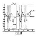
- Fig. 3 is a chart with a horizontal time axis and a vertical amplitude axis, both in arbitrary units, and shows a typical part of the drive signal, labelled "V in (t)".
- V in (t) This consists of constant voltages of either plus one or minus one unit and substantially instantaneous voltage transitions between the constant levels, i.e. a bipolar square wave.
- the minimum interval between transitions is a single clock period.
- the maximum interval will be determined by the random generator 22.
- Many suitable random generators including pseudo-random generators and true, nondeterministic random generators, are known to those skilled in the art.
- random is intended herein to include, without limitation, not only purely random, non-deterministically generated signals, but also pseudo-random and/or deterministic signals such as the output of a shift register arrangement provided with a feedback circuit as used in the prior art to generate pseudo-random binary signals, and chaotic signals.
- the analog output signal V out (t) provided at the terminal 14 is delivered to the processing circuit 16.
- the output signal is first applied to an analog-to-digital converter 26, which samples the output signal 14, each sample being taken in response to a clock pulse at the output of the clock generator 18.
- the delay 20 ensures that each transition in the drive signal will occur at a very short interval after a sampling time.
- the output of the converter 26 is a sequence of samples shown at V out [k] in Fig. 3 , where k is an index representing the position of the sample in the time-ordered sequence. These are delivered to a processor 28 which also receives the output of the random generator 22 (input signal).
- the input signal is also sampled. It is possible to use knowledge of the input signal in subsequent processing, but in practice the effect of the hardware could be such that sampling is desirable. Although sampling of the input signal increases the cost and processing involved, it has advantages, such as in calibration of individual coin testers.
- the processor 28 stores a model which, by suitable choice of model coefficients, can represent the transfer function of the coin sensor 4 when a coin 16 of a specific denomination is located in proximity to the inductance L.
- the model can be developed in a design stage using a knowledge of the physics of the coin sensor by employing any of a number of known techniques.
- H ( s ) and the associated H ( z ) are analog and digital models describing the system.
- the choice of a model (orders p and q) is based on an understanding of the system construction and dynamics.
- PRBS pseudo-random binary sequence
- ARX Auto Regressive with exogenous input.
- the identification can be done in batch mode, which means collecting all the samples from the input and output signals first and then estimating the model coefficients.
- An alternate approach involves using an iterative procedure able to estimate in real time the coefficient set at each new sample pair, such as the RLS (recursive least squares) algorithm.
- OE output error model
- the bridge is balanced for any frequency, including 0, if the two following conditions are met
- the filter (4) is also stable. It should be noticed that there are only 4 filter coefficients dependent on the system components. Yet we have 6 components in the bridge, which means there is an infinite amount of possibility for those leading to the same filter. To reach a one to one mapping between the filter and the analog system we need either to know some components before hand (such the leg #1), or to focus only on time constants and DC gains T 1 , T 2 , G 01 , G 02 , since they appear in both the analog and digital forms. This observation is especially pertinent for identification and a coin recognition point of view.
- a model can then be derived, and then the model parameters are estimated from the samples of the system input and output signals.
- ARMAX Automatic-Regressive Moving Average with Exogenous Input
- the model is then identified, using a batch, or recursive (real time), process and collected data.
- the random bipolar square wave drive signal is applied to the coin sensor 6 as a coin is passing the sensor.
- the input signals, output signals and model are processed, using known techniques as described above, to estimate the model coefficients a 1 , a 2... a p , b 1 , b 2 , ...b q .
- a small set of key co-efficients such as 10 to 20, can capture the overall system dynamic.
- the processor will obtain a plurality of coefficients which will be dependent upon the properties of the coin 16 measured by the coin sensor.
- Acceptance criteria (which could have been derived during a previous training operation) are applied to the coefficients to determine whether the coin is a genuine coin belonging to a particular denomination. Different acceptance criteria can be used for different coin denominations.
- distance e.g. Mahalanobis distance
- discriminant analysis e.g. support vector machines, etc.
- the acceptance criteria may be based on feature vectors derived from model coefficients derived using the techniques described above for known examples of given denominations of coins. Methods for deriving acceptance criteria from known examples are well-known.
- the above operation is carried out for the given coin, and the co-efficients of the model are estimated as described above. All the co-efficients, or a predetermined sub-set of co-efficients, are then used to create an n-dimensional feature vector, which can then be used to validate the coin using the acceptance criteria and known classification techniques.
- measurement values are derived from the converter 26 when applying the drive signal while no coin is in proximity to the inductance L. Then, during the coin measurement stage, the output values derived from the converter 26 have subtracted from them the corresponding idle measurement values before being used for the coefficient adjustment operation.
- corresponding means that the measurements are made at the same time in relation to the random drive signal sequence. This requires that the same random sequence be used during the idle measurements and during the coin testing phases; this can readily be achieved by suitable choice of the random generator 22.
- bridge which is unbalanced in the absence of a coin.
- the measurements used by the processor 28 may all be derived while the coin is substantially at a predetermined location with respect to inductance L, for example, at the mid-point of the coin's travel past a coil forming the inductance L.
- the sample rate is sufficiently high (the clock 18 may for example have a frequency exceeding 1 MHz) that many measurements are taken before the coin has travelled a significant distance.
- the processor 28 uses measurements taken while the coin is travelling over a certain distance. For example, for each of a plurality of successive measurement intervals, the measurements obtained during that interval are used to derive a set of coefficients for the stored model. Accordingly, for each coefficient there will be a sequence of changing values correlated with the different transfer functions as the coin approaches and then leaves the inductance L. Acceptance criteria may be applied to all coefficient sequences. Preferably, a normalisation technique would be used to compensate for varying coin speeds. In other words, the above techniques can be used to derive sets of coefficients for different portions of the coin, as they pass the sensor, taking into account the position of the coin relative to the sensor.
- the drive signal is a bipolar square wave with randomly-selected intervals between signal transitions.
- these features of the drive signal are not essential. It is preferred that the signal be bipolar in order to eliminate DC offset and thus reduce wasted energy, but this is not essential. It is preferred to take measurements during both states of the (binary) input signal, but this also is not essential.
- the signal may take a different shape (e.g. triangular), so long as a sufficiently wide spectrum of frequencies is contained within the signal. If a square wave is used, it may adopt more than two amplitude levels. In any event, preferably the drive signal is a piecewise signal with randomly-selected intervals between transitions.
- the model had model orders p and q.
- these values which determine the number of coefficients calculated during the classification stage, are fixed. However, this is not essential. Instead, the model numbers can be varied in dependence on certain conditions. For example, assuming that the processor is arranged to check whether a coin belongs to one of a number of different target coin classes, the model orders may be varied in dependence on which target class is being checked. Alternatively or additionally, the processor 28 may perform a pre-classification based on, for example, the output of a different coin sensor or a preliminary analysis of the output of the inductance L, and then change the model orders p, q in dependence on this pre-classification process. In one particular example, the model orders may be increased if a pre-classification process indicates that there is likelihood that the coin being tested is a bicolour coin, to account for the more complex nature of the transfer function of the combined sensor and coil.
- one model may be used, or more than one model may used, and similarly any given model may vary.
- the model structure such as the orders p and q could evolve, and be changed as well.
- the embodiment uses an inductive sensor.
- the described processing and modelling techniques can be applied to other types of sensors, such as capacitive and RF sensors, and the corresponding inputs/outputs.
- co-efficients from the models are used for validation/denomination.
- other values derived from the co-efficients can be used.
- data derived from the corresponding frequency spectrum can be used.
- a set, sub-set, or sub-band of frequencies, and the corresponding amplitudes can be selected.
- Frequency information may be especially useful in the context of coin recognition, because frequency is related to depth of penetration within the coin of eddy currents.
- Coefficients, or other related data, such as frequency data can be further processed, such as by averaging, before being applied to acceptance criteria.
- the mapping of a digital model to a corresponding frequency spectrum involves known techniques, see, for example, An Introduction to the Analysis and Processing of Signals by Paul Lynn, 1973 .
- the digital spectrum takes the Z transform of the model and replaces Z by E ⁇ (i*2*pi*f*dt), where dt is the sampling rate, i the imaginary number.
- dt is the sampling rate
- i the imaginary number.
- An advantage of the related analog and digital system models is that the filter co-efficients can be used to derive an analog frequency spectrum, which avoids frequency aliasing problems in the digital model.
- MIMO multiple input multiple output
- Such techniques could be used, for example, for processing more then one sensor (such as coil) at the same time.
- a coin tester may include a small coil for material and thickness detection and a larger coil for diameter measurement. Since there is likely to be interference (cross-talk) between the sensors, a MIMO model (ARMAX, OE, etc) can be used to modelize the whole system including the cross link between sensors.
- coin validators any coin (whether valid or counterfeit), token, slug, washer, or other metallic object or item, and especially any metallic object or item which could be utilised by an individual in an attempt to operate a coin-operated device or system.
- a "valid coin” is considered to be an authentic coin, token, or the like, and especially an authentic coin of a monetary system or systems in which or with which a coin-operated device or system is intended to operate and of a denomination which such coin-operated device or system is intended selectively to receive and to treat as an item of value.
Landscapes
- Physics & Mathematics (AREA)
- General Physics & Mathematics (AREA)
- Investigating Or Analyzing Materials By The Use Of Magnetic Means (AREA)
- Testing Of Coins (AREA)
Claims (15)
- Procédé de test d'une pièce de monnaie à l'aide d'au moins un capteur de pièce de monnaie (4) qui fonctionne en réponse à un signal d'attaque respectif et un processeur (28), le procédé comprenant :l'attaque du/des capteur(s) de pièce de monnaie (4) en utilisant le signal/les signaux d'attaque et l'obtention de multiples échantillons de mesure en provenance du/des capteur(s) en présence de la pièce de monnaie ;caractérisé en ce que le processeur stocke au moins un modèle qui représente la fonction de transfert du/des capteur(s) de pièce de monnaie (4) en présence de la pièce de monnaie ; et parl'obtention des coefficients du modèle de la fonction de transfert en utilisant les échantillons de mesure ; etl'application de critères d'acceptation en utilisant les coefficients pour déterminer si la pièce de monnaie appartient à une classe prédéterminée de pièces de monnaie.
- Procédé selon la revendication 1, comprenant l'étape consistant à appliquer le signal/les signaux d'attaque à large bande au modèle.
- Procédé selon la revendication 1 ou la revendication 2, dans lequel l'au moins un signal d'attaque présente au moins un paramètre aléatoire déterminé, et dans lequel l'au moins un signal d'attaque est un signal par morceaux présentant des transitions à des instants déterminés aléatoirement.
- Procédé selon la revendication 3, dans lequel l'au moins un signal d'attaque présente des transitions de tension sensiblement instantanées à des instants déterminés aléatoirement.
- Procédé selon l'une quelconque des revendications précédentes, dans lequel l'au moins un signal d'attaque est un signal à large bande et les échantillons de mesure représentent des effets des variations de courants de Foucault dans la pièce de monnaie en cours de test, lesquelles variations sont influencées par un champ généré en réponse au signal d'attaque.
- Procédé selon l'une quelconque des revendications précédentes, dans lequel le modèle est représenté par une équation de différence de temps.
- Procédé selon la revendication 6, dans lequel l'équation de différence de temps est la suivante :
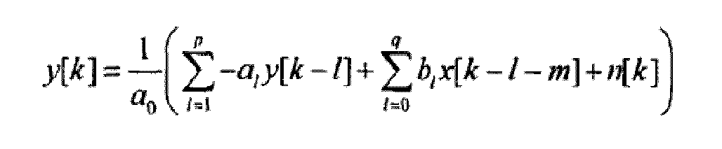
où k est un indice ordonné dans le temps, x[k] et y[k] sont respectivement les échantillons d'entrée et de sortie du capteur, n[k] représente le bruit, p et q sont des ordres prédéterminés du modèle, m est une valeur de retard et ao, a1 et b1 sont des coefficients. - Procédé selon l'une quelconque des revendications précédentes, comprenant l'utilisation des coefficients pour obtenir un spectre de fréquences, et l'application des critères d'acceptation en utilisant des valeurs du spectre de fréquences afin de déterminer si la pièce de monnaie appartient à la classe prédéterminée de pièces de monnaie.
- Procédé selon l'une quelconque des revendications précédentes, dans lequel l'au moins un capteur de pièce de monnaie comprend une bobine unique d'émission/réception combinée.
- Capteur de pièce de monnaie comprenant :une inductance située à proximité d'un trajet des pièces ;un circuit d'attaque (6) conçu pour attaquer l'inductance avec un signal à large bande ;un échantillonneur couplé à l'inductance pour produire des échantillons de mesure successifs ayant des valeurs influencées par les temps des échantillons de mesure par rapport au signal d'attaque à large bande en raison de courants de Foucault induits dans une pièce de monnaie par le champ généré par l'inductance ;dans lequel l'inductance est située dans un bras d'un circuit à courant alternatif en pont ayant une entrée pour recevoir ledit signal d'attaque à large bande et une sortie à partir de laquelle lesdits échantillons de mesure sont obtenus ;caractérisé par un processeur (28) sensible aux échantillons de mesure pour calculer des coefficients d'un modèle de la fonction de transfert du capteur en présence de la pièce de monnaie et pour déterminer si la pièce de monnaie répond à des critères d'acceptation représentant une pièce de monnaie d'une classe particulière.
- Capteur de pièce de monnaie selon la revendication 10, dans lequel le signal d'attaque à large bande est un signal par morceaux, et
dans lequel le signal d'attaque à large bande présente des transitions de tension sensiblement instantanées. - Capteur de pièce de monnaie selon la revendication 11, dans lequel le signal d'attaque à large bande est un signal à onde carrée.
- Capteur de pièce de monnaie selon l'une quelconque des revendications 10 à 12, dans lequel le circuit en pont est un pont de Maxwell.
- Capteur de pièce de monnaie selon l'une quelconque des revendications 10 à 13, dans lequel le circuit en pont est sensiblement équilibré en l'absence de la pièce de monnaie (16).
- Capteur de pièce de monnaie selon l'une quelconque des revendications 10 à 14, dans lequel le processeur (28) est conçu pour obtenir la différence entre chaque échantillon de mesure et un échantillon de repos qui a été obtenu en l'absence d'une pièce de monnaie (16) et avec un cadencement par rapport au signal d'attaque à large bande qui correspond au cadencement de l'échantillon de mesure respectif.
Priority Applications (2)
| Application Number | Priority Date | Filing Date | Title |
|---|---|---|---|
| SI200830894T SI2203902T1 (sl) | 2007-10-23 | 2008-10-20 | Detektor za kovance |
| PL08841778T PL2203902T3 (pl) | 2007-10-23 | 2008-10-20 | Czujnik monet |
Applications Claiming Priority (2)
| Application Number | Priority Date | Filing Date | Title |
|---|---|---|---|
| US11/877,437 US8561777B2 (en) | 2007-10-23 | 2007-10-23 | Coin sensor |
| PCT/US2008/080465 WO2009055333A2 (fr) | 2007-10-23 | 2008-10-20 | Détecteur de pièces de monnaie |
Publications (3)
| Publication Number | Publication Date |
|---|---|
| EP2203902A2 EP2203902A2 (fr) | 2010-07-07 |
| EP2203902A4 EP2203902A4 (fr) | 2011-12-14 |
| EP2203902B1 true EP2203902B1 (fr) | 2012-11-21 |
Family
ID=40562347
Family Applications (1)
| Application Number | Title | Priority Date | Filing Date |
|---|---|---|---|
| EP08841778A Not-in-force EP2203902B1 (fr) | 2007-10-23 | 2008-10-20 | Détecteur de pièces de monnaie |
Country Status (6)
| Country | Link |
|---|---|
| US (1) | US8561777B2 (fr) |
| EP (1) | EP2203902B1 (fr) |
| ES (1) | ES2400025T3 (fr) |
| PL (1) | PL2203902T3 (fr) |
| SI (1) | SI2203902T1 (fr) |
| WO (1) | WO2009055333A2 (fr) |
Cited By (1)
| Publication number | Priority date | Publication date | Assignee | Title |
|---|---|---|---|---|
| EP3287991A1 (fr) | 2017-07-11 | 2018-02-28 | Azkoyen, S.A. | Détecteur de pièces de monnaie |
Families Citing this family (4)
| Publication number | Priority date | Publication date | Assignee | Title |
|---|---|---|---|---|
| EP2826026A1 (fr) * | 2012-03-14 | 2015-01-21 | MEI, Inc. | Capteur de pièce de monnaie |
| CN104813369B (zh) * | 2012-10-25 | 2018-01-12 | 魅股份有限公司 | 将有价值物品分类的系统 |
| JP6425878B2 (ja) * | 2013-10-18 | 2018-11-21 | 株式会社日本コンラックス | 硬貨処理装置 |
| GB2601158B (en) * | 2020-11-20 | 2025-05-21 | Elcometer Ltd | Coating thickness measurement instrument |
Family Cites Families (23)
| Publication number | Priority date | Publication date | Assignee | Title |
|---|---|---|---|---|
| US3576244A (en) * | 1969-01-08 | 1971-04-27 | Vendo Co | Coin acceptor having resistivity and permeability detector |
| US4254857A (en) * | 1978-09-15 | 1981-03-10 | H. R. Electronics Company | Detection device |
| JPS5958595A (ja) * | 1982-09-28 | 1984-04-04 | 富士電機株式会社 | 硬貨選別装置 |
| GB8303587D0 (en) * | 1983-02-09 | 1983-03-16 | Chapman Cash Processing Ltd | Coin discriminating apparatus |
| DE3906448C1 (fr) * | 1989-03-01 | 1990-03-15 | Messerschmitt-Boelkow-Blohm Gmbh, 8012 Ottobrunn, De | |
| JP2767278B2 (ja) * | 1989-04-10 | 1998-06-18 | 株式会社日本コンラックス | 硬貨選別装置 |
| GB2235559A (en) | 1989-08-21 | 1991-03-06 | Mars Inc | Coin testing apparatus |
| WO1993007589A1 (fr) * | 1991-09-28 | 1993-04-15 | Anritsu Corporation | Dispositif pour le triage des pieces de monnaie |
| CA2113492A1 (fr) * | 1994-01-14 | 1995-07-15 | Donald W. Church | Appareil et methode servant a identifier les jetons metalliques et les pieces de monnaie |
| EP0825495B1 (fr) * | 1995-04-26 | 2002-08-14 | Hitachi, Ltd. | Dispositif d'impression electrophotographique |
| JP3258245B2 (ja) | 1996-11-27 | 2002-02-18 | キヤノン電子株式会社 | 硬貨識別装置 |
| US6325197B1 (en) * | 1999-02-25 | 2001-12-04 | Kabushiki Kaisha Nippon Conlux | Method and device for checking coin for forgery |
| JP3773689B2 (ja) * | 1999-03-17 | 2006-05-10 | 株式会社日本コンラックス | コイン検査方法及び装置 |
| GB2359176B (en) * | 2000-02-09 | 2002-08-28 | Tetrel Ltd | Coin validation arrangement |
| ES2170678B1 (es) * | 2000-06-30 | 2003-09-16 | Azkoyen Medios De Pago Sa | Metodo y aparato de obtencion de caracteristicas fisicas de monedas para su identificacion. |
| KR20020022433A (ko) | 2000-09-20 | 2002-03-27 | 이혁병 | 이미지 처리기술을 이용한 주화 선별기 |
| WO2002031764A2 (fr) * | 2000-10-13 | 2002-04-18 | Fraunhofer-Gesellschaft zur Förderung der angewandten Forschung e.V. | Procede d'apprentissage supervise dans un reseau de neurones artificiels recurrent |
| US6455825B1 (en) * | 2000-11-21 | 2002-09-24 | Sandia Corporation | Use of miniature magnetic sensors for real-time control of the induction heating process |
| US6892871B2 (en) * | 2002-03-11 | 2005-05-17 | Cummins-Allison Corp. | Sensor and method for discriminating coins of varied composition, thickness, and diameter |
| ES2343730T3 (es) * | 2003-09-24 | 2010-08-09 | Scan Coin Ab | Discriminador de monedas. |
| DE102004020159A1 (de) | 2004-04-24 | 2005-11-17 | National Rejectors, Inc. Gmbh | Verfahren zum Prüfen von Münzen |
| WO2007070927A1 (fr) * | 2005-12-20 | 2007-06-28 | Minelab Electronics Pty Limited | Plate-forme de detection de metaux en temps reel par transmission d’ondes rectangulaires dotee de proprietes de transmission et de reception selectionnables par un utilisateur |
| GB2437351A (en) * | 2006-04-20 | 2007-10-24 | Agilent Technologies Inc | Broadband transfer function synthesis using orthonormal rational bases |
-
2007
- 2007-10-23 US US11/877,437 patent/US8561777B2/en not_active Expired - Fee Related
-
2008
- 2008-10-20 PL PL08841778T patent/PL2203902T3/pl unknown
- 2008-10-20 ES ES08841778T patent/ES2400025T3/es active Active
- 2008-10-20 SI SI200830894T patent/SI2203902T1/sl unknown
- 2008-10-20 WO PCT/US2008/080465 patent/WO2009055333A2/fr not_active Ceased
- 2008-10-20 EP EP08841778A patent/EP2203902B1/fr not_active Not-in-force
Cited By (2)
| Publication number | Priority date | Publication date | Assignee | Title |
|---|---|---|---|---|
| EP3287991A1 (fr) | 2017-07-11 | 2018-02-28 | Azkoyen, S.A. | Détecteur de pièces de monnaie |
| US10262487B2 (en) | 2017-07-11 | 2019-04-16 | Azkoyen, S.A. | Coin sensor |
Also Published As
| Publication number | Publication date |
|---|---|
| ES2400025T3 (es) | 2013-04-05 |
| SI2203902T1 (sl) | 2013-04-30 |
| PL2203902T3 (pl) | 2013-04-30 |
| US20090101469A1 (en) | 2009-04-23 |
| EP2203902A2 (fr) | 2010-07-07 |
| EP2203902A4 (fr) | 2011-12-14 |
| US8561777B2 (en) | 2013-10-22 |
| WO2009055333A3 (fr) | 2009-07-23 |
| WO2009055333A2 (fr) | 2009-04-30 |
Similar Documents
| Publication | Publication Date | Title |
|---|---|---|
| US20040084278A1 (en) | Coin-validation arrangement | |
| EP2203902B1 (fr) | Détecteur de pièces de monnaie | |
| EP1668602B1 (fr) | Discriminateur de pieces de monnaie | |
| US7548819B2 (en) | Signal measurement and processing method and apparatus | |
| CN112050865A (zh) | 无磁感应测量装置及转动板组件转动信息的计算方法 | |
| US5715926A (en) | Money validation | |
| AU751622B2 (en) | Metal detector method and apparatus | |
| EP1723436B1 (fr) | Procede et appareil de traitement et de mesure du signal | |
| US8820507B2 (en) | Currency discrimination and evaluation | |
| CN109632947A (zh) | 基于传递函数的脉冲涡流检测方法、装置及存储介质 | |
| EP0527874B1 (fr) | Procede et appareil de controle de pieces de monnaie | |
| Jo et al. | A novel feature extraction for eddy current testing of steam generator tubes | |
| US9424703B2 (en) | System to classify an item of value | |
| Enokizono et al. | Crack size and shape determination by moving magnetic field type sensor | |
| Alsabbah et al. | Neural network-based waveguide acoustic gas detector | |
| CN113661390A (zh) | 用于对构件、尤其对喷射器保持体进行检验的方法 | |
| Burtea et al. | Frequency Estimation Using an Artificial Neural Network and the Discrete Fourier Transform | |
| RU2240548C1 (ru) | Устройство для определения октанового числа автомобильного бензина | |
| RU2731320C1 (ru) | Способ обнаружения импульсных помех | |
| Chady et al. | Flaws identification using eddy current differential transducer and artificial neural networks | |
| EP1411480A2 (fr) | Procédé et dispositif pour contrôler des pièces de monnaie ou jetons | |
| AU4752202A (en) | Metal detector method and apparatus | |
| JPH08106564A (ja) | 金属片識別装置 | |
| JPH07118031B2 (ja) | 硬貨判別装置 | |
| GB2422941A (en) | Coin validation |
Legal Events
| Date | Code | Title | Description |
|---|---|---|---|
| PUAI | Public reference made under article 153(3) epc to a published international application that has entered the european phase |
Free format text: ORIGINAL CODE: 0009012 |
|
| 17P | Request for examination filed |
Effective date: 20100424 |
|
| AK | Designated contracting states |
Kind code of ref document: A2 Designated state(s): AT BE BG CH CY CZ DE DK EE ES FI FR GB GR HR HU IE IS IT LI LT LU LV MC MT NL NO PL PT RO SE SI SK TR |
|
| AX | Request for extension of the european patent |
Extension state: AL BA MK RS |
|
| A4 | Supplementary search report drawn up and despatched |
Effective date: 20111116 |
|
| RIC1 | Information provided on ipc code assigned before grant |
Ipc: G01B 7/06 20060101ALI20111110BHEP Ipc: G05B 23/02 20060101ALI20111110BHEP Ipc: G07D 5/00 20060101ALI20111110BHEP Ipc: G07D 5/08 20060101AFI20111110BHEP |
|
| 17Q | First examination report despatched |
Effective date: 20111201 |
|
| RIC1 | Information provided on ipc code assigned before grant |
Ipc: G05B 23/02 20060101ALI20120210BHEP Ipc: G07D 5/00 20060101ALI20120210BHEP Ipc: G01B 7/06 20060101ALI20120210BHEP Ipc: G07D 5/08 20060101AFI20120210BHEP |
|
| GRAP | Despatch of communication of intention to grant a patent |
Free format text: ORIGINAL CODE: EPIDOSNIGR1 |
|
| DAX | Request for extension of the european patent (deleted) | ||
| GRAJ | Information related to disapproval of communication of intention to grant by the applicant or resumption of examination proceedings by the epo deleted |
Free format text: ORIGINAL CODE: EPIDOSDIGR1 |
|
| GRAP | Despatch of communication of intention to grant a patent |
Free format text: ORIGINAL CODE: EPIDOSNIGR1 |
|
| GRAS | Grant fee paid |
Free format text: ORIGINAL CODE: EPIDOSNIGR3 |
|
| GRAA | (expected) grant |
Free format text: ORIGINAL CODE: 0009210 |
|
| RIN1 | Information on inventor provided before grant (corrected) |
Inventor name: BAUDAT, GASTON Inventor name: FURNEAUX, DAVID MICHAEL |
|
| AK | Designated contracting states |
Kind code of ref document: B1 Designated state(s): AT BE BG CH CY CZ DE DK EE ES FI FR GB GR HR HU IE IS IT LI LT LU LV MC MT NL NO PL PT RO SE SI SK TR |
|
| REG | Reference to a national code |
Ref country code: GB Ref legal event code: FG4D |
|
| REG | Reference to a national code |
Ref country code: CH Ref legal event code: EP |
|
| REG | Reference to a national code |
Ref country code: AT Ref legal event code: REF Ref document number: 585422 Country of ref document: AT Kind code of ref document: T Effective date: 20121215 |
|
| REG | Reference to a national code |
Ref country code: IE Ref legal event code: FG4D |
|
| REG | Reference to a national code |
Ref country code: DE Ref legal event code: R096 Ref document number: 602008020332 Country of ref document: DE Effective date: 20130117 |
|
| REG | Reference to a national code |
Ref country code: RO Ref legal event code: EPE |
|
| REG | Reference to a national code |
Ref country code: ES Ref legal event code: FG2A Ref document number: 2400025 Country of ref document: ES Kind code of ref document: T3 Effective date: 20130405 |
|
| REG | Reference to a national code |
Ref country code: NL Ref legal event code: VDEP Effective date: 20121121 |
|
| REG | Reference to a national code |
Ref country code: AT Ref legal event code: MK05 Ref document number: 585422 Country of ref document: AT Kind code of ref document: T Effective date: 20121121 |
|
| PG25 | Lapsed in a contracting state [announced via postgrant information from national office to epo] |
Ref country code: SE Free format text: LAPSE BECAUSE OF FAILURE TO SUBMIT A TRANSLATION OF THE DESCRIPTION OR TO PAY THE FEE WITHIN THE PRESCRIBED TIME-LIMIT Effective date: 20121121 Ref country code: FI Free format text: LAPSE BECAUSE OF FAILURE TO SUBMIT A TRANSLATION OF THE DESCRIPTION OR TO PAY THE FEE WITHIN THE PRESCRIBED TIME-LIMIT Effective date: 20121121 Ref country code: NO Free format text: LAPSE BECAUSE OF FAILURE TO SUBMIT A TRANSLATION OF THE DESCRIPTION OR TO PAY THE FEE WITHIN THE PRESCRIBED TIME-LIMIT Effective date: 20130221 |
|
| REG | Reference to a national code |
Ref country code: PL Ref legal event code: T3 |
|
| PG25 | Lapsed in a contracting state [announced via postgrant information from national office to epo] |
Ref country code: GR Free format text: LAPSE BECAUSE OF FAILURE TO SUBMIT A TRANSLATION OF THE DESCRIPTION OR TO PAY THE FEE WITHIN THE PRESCRIBED TIME-LIMIT Effective date: 20130222 Ref country code: BE Free format text: LAPSE BECAUSE OF FAILURE TO SUBMIT A TRANSLATION OF THE DESCRIPTION OR TO PAY THE FEE WITHIN THE PRESCRIBED TIME-LIMIT Effective date: 20121121 Ref country code: PT Free format text: LAPSE BECAUSE OF FAILURE TO SUBMIT A TRANSLATION OF THE DESCRIPTION OR TO PAY THE FEE WITHIN THE PRESCRIBED TIME-LIMIT Effective date: 20130321 |
|
| PG25 | Lapsed in a contracting state [announced via postgrant information from national office to epo] |
Ref country code: AT Free format text: LAPSE BECAUSE OF FAILURE TO SUBMIT A TRANSLATION OF THE DESCRIPTION OR TO PAY THE FEE WITHIN THE PRESCRIBED TIME-LIMIT Effective date: 20121121 |
|
| PG25 | Lapsed in a contracting state [announced via postgrant information from national office to epo] |
Ref country code: SK Free format text: LAPSE BECAUSE OF FAILURE TO SUBMIT A TRANSLATION OF THE DESCRIPTION OR TO PAY THE FEE WITHIN THE PRESCRIBED TIME-LIMIT Effective date: 20121121 Ref country code: EE Free format text: LAPSE BECAUSE OF FAILURE TO SUBMIT A TRANSLATION OF THE DESCRIPTION OR TO PAY THE FEE WITHIN THE PRESCRIBED TIME-LIMIT Effective date: 20121121 Ref country code: DK Free format text: LAPSE BECAUSE OF FAILURE TO SUBMIT A TRANSLATION OF THE DESCRIPTION OR TO PAY THE FEE WITHIN THE PRESCRIBED TIME-LIMIT Effective date: 20121121 Ref country code: BG Free format text: LAPSE BECAUSE OF FAILURE TO SUBMIT A TRANSLATION OF THE DESCRIPTION OR TO PAY THE FEE WITHIN THE PRESCRIBED TIME-LIMIT Effective date: 20130221 Ref country code: CZ Free format text: LAPSE BECAUSE OF FAILURE TO SUBMIT A TRANSLATION OF THE DESCRIPTION OR TO PAY THE FEE WITHIN THE PRESCRIBED TIME-LIMIT Effective date: 20121121 |
|
| PG25 | Lapsed in a contracting state [announced via postgrant information from national office to epo] |
Ref country code: NL Free format text: LAPSE BECAUSE OF FAILURE TO SUBMIT A TRANSLATION OF THE DESCRIPTION OR TO PAY THE FEE WITHIN THE PRESCRIBED TIME-LIMIT Effective date: 20121121 |
|
| PLBE | No opposition filed within time limit |
Free format text: ORIGINAL CODE: 0009261 |
|
| STAA | Information on the status of an ep patent application or granted ep patent |
Free format text: STATUS: NO OPPOSITION FILED WITHIN TIME LIMIT |
|
| 26N | No opposition filed |
Effective date: 20130822 |
|
| REG | Reference to a national code |
Ref country code: DE Ref legal event code: R097 Ref document number: 602008020332 Country of ref document: DE Effective date: 20130822 |
|
| PG25 | Lapsed in a contracting state [announced via postgrant information from national office to epo] |
Ref country code: HR Free format text: LAPSE BECAUSE OF FAILURE TO SUBMIT A TRANSLATION OF THE DESCRIPTION OR TO PAY THE FEE WITHIN THE PRESCRIBED TIME-LIMIT Effective date: 20130731 |
|
| PGFP | Annual fee paid to national office [announced via postgrant information from national office to epo] |
Ref country code: FR Payment date: 20131009 Year of fee payment: 6 |
|
| PGFP | Annual fee paid to national office [announced via postgrant information from national office to epo] |
Ref country code: SI Payment date: 20130916 Year of fee payment: 6 |
|
| REG | Reference to a national code |
Ref country code: LT Ref legal event code: MM4D Effective date: 20131020 |
|
| PG25 | Lapsed in a contracting state [announced via postgrant information from national office to epo] |
Ref country code: MC Free format text: LAPSE BECAUSE OF FAILURE TO SUBMIT A TRANSLATION OF THE DESCRIPTION OR TO PAY THE FEE WITHIN THE PRESCRIBED TIME-LIMIT Effective date: 20121121 |
|
| REG | Reference to a national code |
Ref country code: CH Ref legal event code: PL |
|
| REG | Reference to a national code |
Ref country code: IE Ref legal event code: MM4A |
|
| PG25 | Lapsed in a contracting state [announced via postgrant information from national office to epo] |
Ref country code: LI Free format text: LAPSE BECAUSE OF NON-PAYMENT OF DUE FEES Effective date: 20131031 Ref country code: LT Free format text: LAPSE BECAUSE OF NON-PAYMENT OF DUE FEES Effective date: 20131020 Ref country code: CH Free format text: LAPSE BECAUSE OF NON-PAYMENT OF DUE FEES Effective date: 20131031 |
|
| PG25 | Lapsed in a contracting state [announced via postgrant information from national office to epo] |
Ref country code: RO Free format text: LAPSE BECAUSE OF NON-PAYMENT OF DUE FEES Effective date: 20121121 |
|
| PG25 | Lapsed in a contracting state [announced via postgrant information from national office to epo] |
Ref country code: LV Free format text: LAPSE BECAUSE OF NON-PAYMENT OF DUE FEES Effective date: 20131020 |
|
| PG25 | Lapsed in a contracting state [announced via postgrant information from national office to epo] |
Ref country code: IE Free format text: LAPSE BECAUSE OF NON-PAYMENT OF DUE FEES Effective date: 20131020 |
|
| REG | Reference to a national code |
Ref country code: PL Ref legal event code: LAPE |
|
| PG25 | Lapsed in a contracting state [announced via postgrant information from national office to epo] |
Ref country code: PL Free format text: LAPSE BECAUSE OF NON-PAYMENT OF DUE FEES Effective date: 20131020 |
|
| PG25 | Lapsed in a contracting state [announced via postgrant information from national office to epo] |
Ref country code: CY Free format text: LAPSE BECAUSE OF FAILURE TO SUBMIT A TRANSLATION OF THE DESCRIPTION OR TO PAY THE FEE WITHIN THE PRESCRIBED TIME-LIMIT Effective date: 20121121 Ref country code: TR Free format text: LAPSE BECAUSE OF FAILURE TO SUBMIT A TRANSLATION OF THE DESCRIPTION OR TO PAY THE FEE WITHIN THE PRESCRIBED TIME-LIMIT Effective date: 20121121 |
|
| PG25 | Lapsed in a contracting state [announced via postgrant information from national office to epo] |
Ref country code: LU Free format text: LAPSE BECAUSE OF NON-PAYMENT OF DUE FEES Effective date: 20131020 Ref country code: HU Free format text: LAPSE BECAUSE OF FAILURE TO SUBMIT A TRANSLATION OF THE DESCRIPTION OR TO PAY THE FEE WITHIN THE PRESCRIBED TIME-LIMIT; INVALID AB INITIO Effective date: 20081020 Ref country code: SI Free format text: LAPSE BECAUSE OF NON-PAYMENT OF DUE FEES Effective date: 20141021 |
|
| REG | Reference to a national code |
Ref country code: FR Ref legal event code: ST Effective date: 20150630 Ref country code: SI Ref legal event code: KO00 Effective date: 20150610 |
|
| PG25 | Lapsed in a contracting state [announced via postgrant information from national office to epo] |
Ref country code: FR Free format text: LAPSE BECAUSE OF NON-PAYMENT OF DUE FEES Effective date: 20141031 Ref country code: MT Free format text: LAPSE BECAUSE OF FAILURE TO SUBMIT A TRANSLATION OF THE DESCRIPTION OR TO PAY THE FEE WITHIN THE PRESCRIBED TIME-LIMIT Effective date: 20121121 |
|
| REG | Reference to a national code |
Ref country code: DE Ref legal event code: R082 Ref document number: 602008020332 Country of ref document: DE Representative=s name: PETERREINS SCHLEY PATENT- UND RECHTSANWAELTE P, DE Ref country code: DE Ref legal event code: R082 Ref document number: 602008020332 Country of ref document: DE Representative=s name: PETERREINS SCHLEY PATENT- UND RECHTSANWAELTE, DE |
|
| PG25 | Lapsed in a contracting state [announced via postgrant information from national office to epo] |
Ref country code: IS Free format text: LAPSE BECAUSE OF FAILURE TO SUBMIT A TRANSLATION OF THE DESCRIPTION OR TO PAY THE FEE WITHIN THE PRESCRIBED TIME-LIMIT Effective date: 20121121 |
|
| PGFP | Annual fee paid to national office [announced via postgrant information from national office to epo] |
Ref country code: DE Payment date: 20181009 Year of fee payment: 11 |
|
| PGFP | Annual fee paid to national office [announced via postgrant information from national office to epo] |
Ref country code: IT Payment date: 20181018 Year of fee payment: 11 Ref country code: ES Payment date: 20181102 Year of fee payment: 11 Ref country code: GB Payment date: 20181017 Year of fee payment: 11 |
|
| REG | Reference to a national code |
Ref country code: DE Ref legal event code: R119 Ref document number: 602008020332 Country of ref document: DE |
|
| PG25 | Lapsed in a contracting state [announced via postgrant information from national office to epo] |
Ref country code: DE Free format text: LAPSE BECAUSE OF NON-PAYMENT OF DUE FEES Effective date: 20200501 |
|
| GBPC | Gb: european patent ceased through non-payment of renewal fee |
Effective date: 20191020 |
|
| PG25 | Lapsed in a contracting state [announced via postgrant information from national office to epo] |
Ref country code: GB Free format text: LAPSE BECAUSE OF NON-PAYMENT OF DUE FEES Effective date: 20191020 Ref country code: IT Free format text: LAPSE BECAUSE OF NON-PAYMENT OF DUE FEES Effective date: 20191020 |
|
| PG25 | Lapsed in a contracting state [announced via postgrant information from national office to epo] |
Ref country code: ES Free format text: LAPSE BECAUSE OF NON-PAYMENT OF DUE FEES Effective date: 20191021 |