EP2204080B1 - Ensembles électriques de montage de composant - Google Patents
Ensembles électriques de montage de composant Download PDFInfo
- Publication number
- EP2204080B1 EP2204080B1 EP08833375A EP08833375A EP2204080B1 EP 2204080 B1 EP2204080 B1 EP 2204080B1 EP 08833375 A EP08833375 A EP 08833375A EP 08833375 A EP08833375 A EP 08833375A EP 2204080 B1 EP2204080 B1 EP 2204080B1
- Authority
- EP
- European Patent Office
- Prior art keywords
- electrical component
- sleeve
- housing
- diameter
- mounting assembly
- Prior art date
- Legal status (The legal status is an assumption and is not a legal conclusion. Google has not performed a legal analysis and makes no representation as to the accuracy of the status listed.)
- Not-in-force
Links
Images

Classifications
-
- H—ELECTRICITY
- H05—ELECTRIC TECHNIQUES NOT OTHERWISE PROVIDED FOR
- H05K—PRINTED CIRCUITS; CASINGS OR CONSTRUCTIONAL DETAILS OF ELECTRIC APPARATUS; MANUFACTURE OF ASSEMBLAGES OF ELECTRICAL COMPONENTS
- H05K13/00—Apparatus or processes specially adapted for manufacturing or adjusting assemblages of electric components
- H05K13/04—Mounting of components, e.g. of leadless components
-
- H—ELECTRICITY
- H05—ELECTRIC TECHNIQUES NOT OTHERWISE PROVIDED FOR
- H05K—PRINTED CIRCUITS; CASINGS OR CONSTRUCTIONAL DETAILS OF ELECTRIC APPARATUS; MANUFACTURE OF ASSEMBLAGES OF ELECTRICAL COMPONENTS
- H05K3/00—Apparatus or processes for manufacturing printed circuits
- H05K3/30—Assembling printed circuits with electric components, e.g. with resistors
- H05K3/301—Assembling printed circuits with electric components, e.g. with resistors by means of a mounting structure
-
- H—ELECTRICITY
- H05—ELECTRIC TECHNIQUES NOT OTHERWISE PROVIDED FOR
- H05K—PRINTED CIRCUITS; CASINGS OR CONSTRUCTIONAL DETAILS OF ELECTRIC APPARATUS; MANUFACTURE OF ASSEMBLAGES OF ELECTRICAL COMPONENTS
- H05K13/00—Apparatus or processes specially adapted for manufacturing or adjusting assemblages of electric components
- H05K13/02—Feeding of components
-
- H—ELECTRICITY
- H05—ELECTRIC TECHNIQUES NOT OTHERWISE PROVIDED FOR
- H05K—PRINTED CIRCUITS; CASINGS OR CONSTRUCTIONAL DETAILS OF ELECTRIC APPARATUS; MANUFACTURE OF ASSEMBLAGES OF ELECTRICAL COMPONENTS
- H05K3/00—Apparatus or processes for manufacturing printed circuits
- H05K3/30—Assembling printed circuits with electric components, e.g. with resistors
-
- H—ELECTRICITY
- H05—ELECTRIC TECHNIQUES NOT OTHERWISE PROVIDED FOR
- H05K—PRINTED CIRCUITS; CASINGS OR CONSTRUCTIONAL DETAILS OF ELECTRIC APPARATUS; MANUFACTURE OF ASSEMBLAGES OF ELECTRICAL COMPONENTS
- H05K7/00—Constructional details common to different types of electric apparatus
- H05K7/02—Arrangements of circuit components or wiring on supporting structure
- H05K7/12—Resilient or clamping means for holding component to structure
-
- H—ELECTRICITY
- H05—ELECTRIC TECHNIQUES NOT OTHERWISE PROVIDED FOR
- H05K—PRINTED CIRCUITS; CASINGS OR CONSTRUCTIONAL DETAILS OF ELECTRIC APPARATUS; MANUFACTURE OF ASSEMBLAGES OF ELECTRICAL COMPONENTS
- H05K2201/00—Indexing scheme relating to printed circuits covered by H05K1/00
- H05K2201/09—Shape and layout
- H05K2201/09818—Shape or layout details not covered by a single group of H05K2201/09009 - H05K2201/09809
- H05K2201/09827—Tapered, e.g. tapered hole, via or groove
-
- H—ELECTRICITY
- H05—ELECTRIC TECHNIQUES NOT OTHERWISE PROVIDED FOR
- H05K—PRINTED CIRCUITS; CASINGS OR CONSTRUCTIONAL DETAILS OF ELECTRIC APPARATUS; MANUFACTURE OF ASSEMBLAGES OF ELECTRICAL COMPONENTS
- H05K2201/00—Indexing scheme relating to printed circuits covered by H05K1/00
- H05K2201/10—Details of components or other objects attached to or integrated in a printed circuit board
- H05K2201/10007—Types of components
- H05K2201/10015—Non-printed capacitor
-
- H—ELECTRICITY
- H05—ELECTRIC TECHNIQUES NOT OTHERWISE PROVIDED FOR
- H05K—PRINTED CIRCUITS; CASINGS OR CONSTRUCTIONAL DETAILS OF ELECTRIC APPARATUS; MANUFACTURE OF ASSEMBLAGES OF ELECTRICAL COMPONENTS
- H05K2201/00—Indexing scheme relating to printed circuits covered by H05K1/00
- H05K2201/10—Details of components or other objects attached to or integrated in a printed circuit board
- H05K2201/10227—Other objects, e.g. metallic pieces
- H05K2201/10325—Sockets, i.e. female type connectors comprising metallic connector elements integrated in, or bonded to a common dielectric support
-
- H—ELECTRICITY
- H05—ELECTRIC TECHNIQUES NOT OTHERWISE PROVIDED FOR
- H05K—PRINTED CIRCUITS; CASINGS OR CONSTRUCTIONAL DETAILS OF ELECTRIC APPARATUS; MANUFACTURE OF ASSEMBLAGES OF ELECTRICAL COMPONENTS
- H05K2201/00—Indexing scheme relating to printed circuits covered by H05K1/00
- H05K2201/10—Details of components or other objects attached to or integrated in a printed circuit board
- H05K2201/10431—Details of mounted components
- H05K2201/10583—Cylindrically shaped component; Fixing means therefore
-
- H—ELECTRICITY
- H05—ELECTRIC TECHNIQUES NOT OTHERWISE PROVIDED FOR
- H05K—PRINTED CIRCUITS; CASINGS OR CONSTRUCTIONAL DETAILS OF ELECTRIC APPARATUS; MANUFACTURE OF ASSEMBLAGES OF ELECTRICAL COMPONENTS
- H05K2201/00—Indexing scheme relating to printed circuits covered by H05K1/00
- H05K2201/10—Details of components or other objects attached to or integrated in a printed circuit board
- H05K2201/10431—Details of mounted components
- H05K2201/1059—Connections made by press-fit insertion
-
- H—ELECTRICITY
- H05—ELECTRIC TECHNIQUES NOT OTHERWISE PROVIDED FOR
- H05K—PRINTED CIRCUITS; CASINGS OR CONSTRUCTIONAL DETAILS OF ELECTRIC APPARATUS; MANUFACTURE OF ASSEMBLAGES OF ELECTRICAL COMPONENTS
- H05K2201/00—Indexing scheme relating to printed circuits covered by H05K1/00
- H05K2201/10—Details of components or other objects attached to or integrated in a printed circuit board
- H05K2201/10431—Details of mounted components
- H05K2201/10606—Permanent holder for component or auxiliary printed circuits mounted on a printed circuit board [PCB]
-
- H—ELECTRICITY
- H05—ELECTRIC TECHNIQUES NOT OTHERWISE PROVIDED FOR
- H05K—PRINTED CIRCUITS; CASINGS OR CONSTRUCTIONAL DETAILS OF ELECTRIC APPARATUS; MANUFACTURE OF ASSEMBLAGES OF ELECTRICAL COMPONENTS
- H05K3/00—Apparatus or processes for manufacturing printed circuits
- H05K3/30—Assembling printed circuits with electric components, e.g. with resistors
- H05K3/306—Assembling printed circuits with electric components, e.g. with resistors with lead-in-hole components
- H05K3/308—Adaptations of leads
-
- Y—GENERAL TAGGING OF NEW TECHNOLOGICAL DEVELOPMENTS; GENERAL TAGGING OF CROSS-SECTIONAL TECHNOLOGIES SPANNING OVER SEVERAL SECTIONS OF THE IPC; TECHNICAL SUBJECTS COVERED BY FORMER USPC CROSS-REFERENCE ART COLLECTIONS [XRACs] AND DIGESTS
- Y10—TECHNICAL SUBJECTS COVERED BY FORMER USPC
- Y10T—TECHNICAL SUBJECTS COVERED BY FORMER US CLASSIFICATION
- Y10T29/00—Metal working
- Y10T29/49—Method of mechanical manufacture
- Y10T29/49002—Electrical device making
- Y10T29/49117—Conductor or circuit manufacturing
- Y10T29/49124—On flat or curved insulated base, e.g., printed circuit, etc.
- Y10T29/4913—Assembling to base an electrical component, e.g., capacitor, etc.
Definitions
- the present invention is directed to an electrical component mounting assembly and to a method of mounting an electrical component such as a capacitor, diode or resistor to a printed circuit board (PCB) or to another mounting member.
- an electrical component such as a capacitor, diode or resistor to a printed circuit board (PCB) or to another mounting member.
- An electrical component mounting assembly with that feature is known from DE 100 62 962 A1 and includes a housing forming a cylindrically shaped receptacle for directly receiving the electrical component which has one predetermined diameter.
- a housing for accommodating electronical components is known from DE 198 29 920 A1 and has, opposite to a printed circuit board, a mounting wall for securing further electronic components of predetermined diameter.
- US 3,086,070 shows mounting of electrical elements in cylindrical housings that include electrically insulating and heat-resistant cup-like members for clamping the electrical elements therebetween.
- a mounting device for semiconductors is known from US 3,146,384 and is made up from a heat dissipating body with a cylindrical opening, a split sleeve and a split ring for clamping a transistor of predetermined diameters therebetween.
- cylindrical electrical components such as electrolytic capacitors are mounted via a housing that has a chamber to receive one of the electrical components.
- housings are typically mounted directly to or flush against the PCB and have openings to allow the passage of the leads of the electrical component for electrical connection to the PCB.
- mounting of these types of housings occupies more space on the PCB which is a valuable commodity.
- some of these applications use an epoxy to retain capacitors to the housing and to prevent dislodgement of the capacitors from the housings due to environmental effects such as vibration, thermal expansion and contraction or deviations in the diameter and/or length of the capacitor.
- the invention is based on the problem of providing a mounting assembly for mounting anyone of a plurality of cylindrical electrical components to a printed circuit board.
- a mounting assembly having a sleeve for receiving a cylindrical electrical component, a housing having a cylindrical chamber that cooperates with the sleeve to securely retain the cylindrical electrical component therein and mounting posts for mounting the housing to a PCB or other mounting member.
- a mounting assembly is disclosed herein that has a housing with a base and a tapered chamber for receiving therein one of a plurality of unique diameter electrical components having a sleeve substantially surrounding each electrical component, typically wherein the housing is mounted to a PCB such that the base of the housing is elevated above the PCB.
- Each sleeve is dimensioned to receive one of the unique diameter electrical components and can accommodate some deviations of the diameter of the electrical component, and the cooperation of the tapered sleeve and tapered chamber securely retains the electrical component to the housing.
- Cylindrical electrical component mounting assemblies of the present disclosure can include a housing with a chamber for receiving a cylindrical electrical component in a horizontal or vertical orientation and have at least two posts for mounting the housing to the PCB in a predetermined raised position above the surface of the PCB or flush against the PCB.
- the electrical component mounting assemblies disclosed herein secure the electrical component to the housing without the use of epoxy or other adhesive compounds through use of a cooperating tapered sleeve and a tapered housing chamber.
- the sleeve can have a passage or opening extending the length of the sleeve, and the sleeve can be dimensioned to accept electrical components having a common diameter.
- the sleeve can exhibit resilient closeability both to accommodate variation or deviation in the electrical component's diameter and to compress about the electrical component to retain it within the housing.
- the electrical component mounting assemblies can reduce the complexity of having a different housing for every differently sized electrical component by providing one housing that can secure electrical components having different diameters and their associated sleeves.
- electrical mounting assemblies as described herein can have a housing that securely accepts one of a plurality of unique diameter electrical components and their associated sleeves.
- the housing can also include a terminal support structure for supporting termination contacts for electrically connecting the leads of the electrical component to the PCB.
- the termination contacts can be selected from those requiring soldering to both the leads and the PCB or those having mechanical solderless connection to one or both the leads and the PCB.
- an electrical component mounting assembly for mounting any one of a plurality of cylindrical electrical components to a mounting member with each electrical component having a unique diameter.
- the electrical component mounting assembly comprises a sleeve for each unique diameter cylindrical electrical component and a housing having a tapered chamber dimensioned to accept one of a plurality of unique diameter cylindrical electrical components received within their associated sleeves.
- the sleeve has an inner surface defining a substantially cylindrical opening for snugly receiving the unique diameter cylindrical component and an outer surface tapered inward from a first end to a second end and the tapered chamber has an entrance end having a diameter greater than the diameter of a back end; wherein progressive insertion of the second end of the sleeve through the entrance end and into the tapered chamber causes the sleeve to compress against the unique diameter cylindrical electrical component and to frictionally retain the unique diameter cylindrical electrical component and its associated sleeve to the housing.
- a capacitor mounting assembly for mounting any one of a plurality of uniquely diametered capacitors to a PCB.
- the capacitor mounting assembly comprises a sleeve for each uniquely diametered capacitor and a housing having a tapered chamber dimensioned to separately accept a plurality of uniquely diametered capacitors and their associated sleeves.
- the sleeve has an inner surface defining a substantially cylindrical opening for snugly receiving the uniquely diametered capacitor and an outer surface tapered inward from a first end to a second end.
- the tapered chamber has an entrance end having a diameter greater than the diameter of a back end; wherein progressive insertion of the second end of the sleeve through the entrance end and into the tapered chamber causes the sleeve to compress against the uniquely diametered capacitor and to frictionally retain the uniquely diametered capacitor and its associated sleeve to the housing.
- an electrical component mounting assembly for mounting an electrical component to a mounting member.
- the electrical component mounting assembly comprises a tapered sleeve having a first end wider than a second end and defining an opening for snugly receiving an electrical component therein and a housing having a tapered chamber for accepting the sleeve and electrical component.
- the tapered chamber has a entrance end and back end opposite to the entrance end and the entrance end is wider than the back end; wherein progressive insertion of the narrow end of sleeve through the entrance end and into tapered chamber causes the sleeve to compress against the electrical component and to frictionally retain the sleeve and electrical component to the housing.
- an electrical component holder for fastening an electrical component to a mounting member having a plurality of receiving openings therein.
- the electrical component holder comprises a housing having a generally cylindrical retention area with the retention area having a generally cylindrical body portion extending around a central axis and a generally flat base along one side of the body portion.
- the housing has an open front end to receive the electrical component and an opposite back end.
- the electrical component holder also comprises a plurality of support members extending from the base.
- the support members each have an insert portion to be received within a respective receiving opening in the mounting member and a spacer portion between the insert portion and the retention area for spacing the retention portion a predetermined distance above the mounting member when the insert portions are received within the receiving openings in the mounting member.
- the spacer portions are spaced apart to provide a component retention area below the base wherein additional components can be mounted to the PCB below the retained capacitor.
- a method of mounting an electrical component to a mounting member comprises the steps of inserting the electrical component in a passage defined by an inner surface of a sleeve having an outer surface tapered inward from a first end to a second end; inserting the sleeve having the electrical component received therein, second end first, into a tapered chamber of a housing to engage a friction fit taper lock between the tapered outer surface of the sleeve and the tapered chamber with the tapered chamber narrowing from an entrance end to a back end; and inserting a plurality of posts of the housing into respective receiving openings of the mounting member.
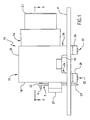
- Fig. 1 is an elevation view of one embodiment of the electrical component mounting assembly of the present disclosure mounted to a PCB.
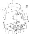
- Fig. 2 is a perspective view of the electrical component mounting assembly shown in Fig. 1 .
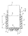
- Fig. 3 is a cross-sectional view of the electrical component mounting assembly shown in Fig. 1 taken at line 3-3.
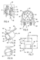
- Fig 4 is a perspective view of the rear wall of the housing of the electrical component assembly shown in Fig. 1 showing lead extensions supported in extension clips of the termination support shelf.
- Fig. 5 is an elevation view of the front end of the housing of the electrical component mounting assembly shown in Fig. 1 .
- Fig. 6 is a perspective view of the sleeve of the electrical component mounting assembly of Fig. 1 .
- Fig. 7 is an elevation view of a top side of the sleeve shown in Fig. 6 .
- Fig. 8 is an elevation view of a front end of the sleeve shown in Fig. 6 .
- Fig. 9 is an elevation view of a front end of another embodiment of a housing of the electrical component mounting assembly of the present disclosure.
- Fig, 10 is an elevation view of the side of the housing shown in Fig. 9 .
- Fig. 11 is an elevation view of the front end of another embodiment of a sleeve of the electrical component mounting assembly of the present disclosure.
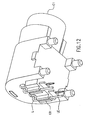
- Fig. 12 is a perspective view of another embodiment of an electrical mounting assembly including the housing shown in Fig. 9 and the sleeve shown in Fig. 11 .
- Fig. 1 illustrates one embodiment of electrical component mounting assembly 10 of the present disclosure for attaching a cylindrical electrical component such as capacitor “C1” to PCB "P". While mounting assembly 10 will be shown mounting capacitor “C1” in all the following illustrations it will be understood that mounting assembly 10 can mount other cylindrical electrical components such as diodes, resistors, transistors and the like and that the mounting can be made to a PCB as illustrated or to some other mounting member. Mounting assembly 10 can have housing 12 and sleeve 14 placed around a capacitor “C1” which cooperates with housing 12 to retain capacitor “C1” to housing 12. Capacitor “C1” is mounted to PCB “P” in a longitudinal orientation that is horizontal as illustrated in Fig. 1 .
- housing 12 can mount an electrical component in a vertical orientation as well. As shown in Figs. 1 and 2 , housing 12 can have base wall 16, rear wall 18 extending substantially perpendicularly to base wall 16, and substantially cylindrical body portion 20. Housing 12 can have posts 22 and latching bars 24, all of which can extend downward from base wall 16. Posts 22 and latch bars 24 can be received in appropriately dimensioned holes (not shown) in PCB "P" for mounting housing 12 to PCB "P" such that base wall 16 is raised above PCB "P", as shown in Fig. 1 ..
- Latching bars 24 provide "press fit” locking to PCB "P", and for reinforced mounting or instead of mounting the assembly 10 with latch bars 24, insertion portions 21 of posts 22 can be heat staked to PCB "P" using known methods.
- Between base wall 16 and insertion portion 21 of posts 22 can be spacer portions 23.
- each spacer portion 23 has a wider profile than insertion portion 21 that operates as a stop surface against PCB.
- posts 22 can have a stop surface to engage PCB to elevate base wall 16 from PCB.
- Insertion portions 21 can be inserted through holes (not shown) of PCB board only up to spacer portions 23. This effectively raises base wall 16 above PCB board.
- the spacer portions can be dimensioned to permit a desired elevation of the housing to allow either additional components to be mounted under housing 12 or to allow circuit traces to run beneath housing 12.
- the raised horizontal positioning of the capacitor, as described, provides a generally low-profile design which also increases available PCB mounting space for component placement.
- housing 12 can be mounted such that base wall 16 is flush against PCB which permits an even lower profile but does not provide the intermediate space for additional components or circuit traces.
- Hook portion 26 of latching bars 24 can be positioned slightly below spacer portions 23 so that when housing 12 is pushed against PCB "P" latch bars 24 can lock to PCB "P" before spacer portions 23 contact PCB "P".
- the vertical distance between hook portion 26 and spacer portions 23 can determine the degree of vertical movement of housing 12 relative to PCB "P".
- housing 12 can be mounted to PCB "P” only by heat staking posts 22 to PCB "P” or only with latch bars 24. While housing 12 shown in Figs. 1 and 2 has four posts 22 and four latch bars 24, housing 12 can have two or more posts 22, two or more latch bars 24, or one or more of each of post 22 and latch bar 24.
- Rear wall 18 can have two apertures 25 for allowing leads “L” to exit housing 12 when capacitor “C1" is inserted into housing 12 as shown in Figs. 2 and 3 .
- Termination support shelf 27 shown in Fig. 2 can extend from rear wall 18 and can include one or more terminal slots 29 for receiving terminal connectors "T” having compliant push pins "CP” at one end for solderless press-fit type electrical connection to the PCB "P” and lead clips "LC” at an opposite end for connection with the exiting leads "L”.
- Termination support shelf 27 can also have one or more extension clips 31. Extension clips 31 can support lead extensions "LE" (see Fig.
- Housing 12 can be modified to mount an electrical component in a vertical orientation by repositioning posts 22 relative to substantially cylindrical body portion 20 such as having substantially cylindrical body portion 20 extend in parallel orientation to posts 22 and/or latch bars 24 as opposed to perpendicular orientation shown in Fig. 1 .
- terminal connectors "T” may be altered such that push pins "CP” extend in parallel relation to leads "L".
- housing 12 can have a substantially cylindrical tapered retention area or chamber 30 to receive capacitor "C1".
- Inner cylindrical wall 32 of housing 12 can taper inward from entrance 34 to interior surface 36 of rear wall 18 to form tapering or narrowing chamber 30.
- entrance diameter "D1" of chamber 30 at entrance 34 is greater than interior diameter "D2" of chamber 30 at interior surface 36 of rear wall 18.
- Sleeve 14 can have tapered outer surface 28 that cooperates with tapered chamber 30 to clamp or compress against capacitor "C1" as sleeve 14 is inserted into housing 12 to hold capacitor "C1", which is retained in sleeve 14, within housing 12 as shown in Fig. 3 .
- the lack of appreciable expansion of housing 12 creates a tight friction fit of sleeve 14 to housing 12 to retain sleeve 14 in housing 12.
- slot 40 can extend from outside end 42 to insertion end 44 of sleeve 14. Slot 40 and the material of the sleeve cooperate to provide flexibility or resilient closeability to the sleeve and allows sleeve 14 to clamp against capacitor "C1".
- the cooperating taper of sleeve 14 and tapered chamber 30 increases the clamping force of sleeve 14 against capacitor "C1" as sleeve 14 progresses into chamber 30.
- the degree of tapering of outer surface 28 and chamber 30 can be balanced between providing sufficient surface contact of outer surface 28 and chamber 30 to produce the desired retaining force and the ability to retain a desired range of electrical components having different diameters. In general, it will be understood that the closer the tapering of the outer surface 28 and chamber 30 match each other, the greater the amount of surface contact. In one embodiment, the degree of tapering of the outer surface 28 is the same as the degree of tapering of chamber 30. In another embodiment, chamber 30 and outer surface 28 can each taper from between about 0.5 degrees to about 5 degrees. In yet another embodiment, chamber 30 and outer surface 28 can each taper from about 1 degree to about 3 degrees. In the illustrated embodiments, chamber 30 and outer surface 28 both can taper about 2 degrees from the axis of the chamber 30 and sleeve 14, respectively.
- Housing 12 and sleeve 14 can each be made from the same or from different materials. Thermoplastic materials are typically utilized. In one embodiment both housing 12 and sleeve 14 are constructed of polyamide material such as nylon PA6 30% glass-filled material. While having the sleeve 14 and housing 12 constructed from the same material is not necessary, this arrangement benefits from having a more uniform thermal expansion or contraction which can reduce the risk of loosening the taper lock frictional attachment of the sleeve 14 to the housing 12. Also, having sleeve 14 and housing 12 be uniformly tapered provides a uniform cross-sectional thickness for consistent expansion/contraction which may be caused by temperature change.
- sleeve 14 can have plank 48 extending from insertion end 44 at a side opposite slot 40.
- Plank 48 is dimensioned to extend through slot 50 in rear wall 18 of housing 12 when sleeve 12 is inserted into housing 12.
- Plank 48 can be heat staked as shown in Fig. 2 to reinforce the friction fit retention of sleeve 14 to housing 12. Heat staking can be accomplished by known methods.
- Sacrificial key 52 can extend from outer surface 28. As will be described in the assembly process below, sacrificial key 52 can be used to pick and place sleeve 14 during the process of fastening capacitor "C1" to sleeve 14 and housing 12 and is removed after assembly. Sacrificial key 52 can have a head portion 54 and a neck portion 56 attaching head 54 to outer surface 28.
- Tapered outer surface 28 can taper inward from outside end 42 to insertion end 44 as shown in Fig 7 . This results in outer diameter "D3" measured at outer surface 28 at outside end 42 being greater than outer diameter "D4" measured at outer surface 28 at insertion end 44. As shown in Fig. 8 , inner diameter "D5" measured at inner surface 60 of sleeve 14 can be substantially the same at both insertion end 44 and outside end 42 to provide a substantially uniform cylindrical receiving opening or passage. This uniform cylindrical receiving opening is also shown in Fig. 3 . It is understood that having a uniform cylindrical receiving opening or uniform diameter "D3" and a tapered outer surface 28 results in sleeve wall 62 being thicker at outside end 42 than at insertion end 44.
- sleeve 14 can be dimensioned specifically for each capacitor diameter.
- each capacitor having a unique diameter can be fastened to housing 12 using sleeve 14 having dimensions specifically for that unique diameter capacitor.
- the length of the capacitor or other electrical component however may not affect the dimensions of the sleeve 14, particularly if these electrical components have standard as opposed to custom lengths.
- Inner diameter "D5" can be manufactured to be slightly less than the capacitor to be retained. Slot 40 allows sleeve 14 to open and accept the electrical component, and due to the resilient closeability of the sleeve material, the electrical component can be held firmly in sleeve 14.
- "D5" can be from about 1% to about 20% less than the diameter of the electrical component to be retained.
- "D5" can be from about 3% to about 15% less than the diameter of the electrical component to be retained.
- Housing 12 typically is dimensioned to mount more than one capacitor or other electrical component diameter size.
- Chamber 30 can be dimensioned to securely retain the largest diameter electrical component desired to be mounted to PCB "P" by cooperation of chamber 30 and the particular electrical component's associated sleeve 14 as described above.
- the dimensions of sleeve 14 can be varied to securely retain such components in chamber 30.
- the dimensions of sleeve 14 can be varied by reducing inner diameter "D5" according to the diameter of the electrical component to be retained as described above and the thickness of wall 62 can be increased such that outer surface 28 and tapered chamber 30 cooperate as described above.
- housing 12 can be dimensioned to securely retain the largest diameter electrical component by making diameter "D1" greater than diameter "D4" of the largest component diameter sleeve 14 but less than diameter "D3", and diameter "D2" can be less than diameter "D4".
- housing 12 mount less than all of the various diameter electrical components.
- multiple housings 12 can be used to accommodate all the various sizes of electrical component diameters.
- the lengths of some of the capacitors to be mounted make having only one housing 12 mount them all impractical because some capacitors may extend either too far out of or to far into the housing for the desired application.
- having all housings 12 dimensioned for the largest diameter capacitor to be mounted may take up more space on the PCB than necessary, especially when there are a greater number of smaller diameter capacitors than larger diameter capacitors.
- housing 12 is dimensioned to securely retain and to mount either of two capacitors having two different diameters to the PCB "P".
- housing 12 can be dimensioned to securely retain 16 mm and 18 mm diameter capacitors having a length that ranges from 15 mm to 40 mm, or to retain 10 mm and 12.5 mm diameter capacitors having a length that ranges from 12.5 mm to 25 mm.
- housing 12 can have diameter "D1" of about 15.2 mm, diameter "D2" of about 14.1 mm.
- sleeve 14 can be 13.6 mm and chamber 30 can taper at an angle of about 2 degrees.
- the following dimensions of sleeve 14 for each of the 10 mm and 12.5 mm capacitors are the same except for diameter "D5" which can be about 9 mm for 10 mm diameter capacitors and about 11.5 mm for 12.5 mm diameter capacitors.
- Length "L3" of sleeve 14 from outside end 42 to insertion end 44 can be about 14 mm
- length "L4" of sleeve 14 including plank 48 can be about 26.3 mm
- housing 12 can have diameter "D1" of about 20.8 mm, diameter "D2" can be about 19.3 mm.
- the length of tapered chamber 30 "L1" from entrance 34 to interior surface 36 of rear wall 18 shown in Fig. 3 can be 19.8 mm and chamber 30 can taper at an angle of about 2 degrees.
- the following dimensions of sleeve 14 for each of the 16 mm and 18 mm capacitors are the same except for diameter "D5" which can be about 17 mm for 18 mm diameter capacitors and about 15 mm for 16 mm diameter capacitors.
- Length "L3" of sleeve 14 from outside end 42 to insertion end 44 can be about 20 mm
- length "L4" of sleeve 14 including plank 48 can be about 37.5 mm
- housing 112 can have base wall 116 and rear wall 118 extending substantially perpendicular from base wall 116.
- Substantially cylindrical body portion 120 can join rear and base walls 116, 118, respectively.
- Termination support shelf 127 can extend from the rear wall 118.
- Four posts 122 can extend downward from base wall and have spacer portions 123 for elevating base wall 116 above PCB a predetermined distance and insertion portions 121 which can be received in holes (not shown) of a PCB and heat staked for secure mounting to the PCB as discussed above with respect to housing 12.
- housing 112 is substantially similar to housing 12 in many respects, one variation can be that substantially cylindrical tapered chamber 130 can have a flat base surface 170. This can assist in reducing the overall height of housing 112 to compensate somewhat for spacer portions 123.
- Another embodiment of sleeve 114 shown in Fig. 11 can have flat edges 172 to correspond to flat base surface 170 housing 112.
- Termination support shelf 127 of housing 112 shown in Fig. 12 can have extension clips 131.
- Lead extension "LE” can be supported in clips 131 and can be soldered to the PCB at one end and to leads “L” of capacitor “C1" at the other end.
- a mechanical connection can be used to connect leads “L” to lead extensions “LE” as shown in Fig. 4 .
- Sacrificial key 54 of sleeve 14 is used to pick and place sleeve 14 on an assembly track.
- a capacitor is inserted into a preload position with sleeve 14.
- the preload position depends on the length of the electrical component to be mounted but, typically, sleeve 14 is positioned off-center towards the front end of the capacitor which is opposite the lead end (i.e. the end from which the leads extend) of the capacitor "C1".
- Housing 12 is inserted over the sleeve 14 and capacitor "C1" until lead end of capacitor "C1" contacts interior surface 36 of rear wall 18 ( Fig. 3 ).
- the tapered outer surface 28 of sleeve 14 should not, at this point, fully lock with tapered chamber 30. If this occurs, sleeve 14 should be positioned further off-center towards front end of capacitor "C1". Sleeve 14 can then be pushed into housing 12 to engage taper lock between outer surface 28 and chamber 30. Plank 48 can be cut and heat staked to housing 12. Depending on the type of electrical connection to be made between leads "L” and the PCB or other mounting member terminals "T” can be inserted into slots 29 prior to placing sleeve 14 and capacitor "C1" into the housing.
- leads “L” can be mechanically connected to lead clips "LC” of terminals “T” or lead extensions "LE” can be soldered to leads “L” and clipped to extension clips 31.
- Sacrificial key 54 can then be removed.
Landscapes
- Engineering & Computer Science (AREA)
- Microelectronics & Electronic Packaging (AREA)
- Manufacturing & Machinery (AREA)
- Structures For Mounting Electric Components On Printed Circuit Boards (AREA)
- Mounting Components In General For Electric Apparatus (AREA)
- Casings For Electric Apparatus (AREA)
- Details Of Connecting Devices For Male And Female Coupling (AREA)
Claims (19)
- Ensemble de montage pour composant électrique pour monter un composant électrique sur une carte de circuit imprimé, comprenant :un boîtier (12) ayant des moyens pour supporter et fixer le boîtier sur une carte de circuit imprimé (P) et un manchon (14) pour loger le composant électrique (C1),dans lequel le boîtier (12) comprend une chambre (30) pour recevoir le manchon (14), caractérisé en ce quela chambre (30) est progressivement rétrécie d'une extrémité ouverte (34) à une extrémité arrière (36), et en ce queon prévoit une pluralité de manchons (14), chacun dimensionné pour accepter l'un d'une pluralité de composants électriques à diamètre unique, chaque manchon (14) ayant une surface externe (28) progressivement rétrécie pour être inséré dans l'extrémité ouverte (34) de la chambre progressivement rétrécie (30), chaque manchon (14) ayant également une surface interne pour fournir un passage de réception (60) sensiblement cylindrique afin de recevoir les composants électriques (C1) respectifs,dans lequel l'insertion progressive du manchon (14) dans la chambre progressivement rétrécie (30) amène le manchon à se comprimer contre le composant électrique cylindrique à diamètre unique et son manchon associé au boîtier.
- Ensemble de montage pour composant électrique selon la revendication 1,
dans lequel le composant électrique (C1) cylindrique est un condensateur électrolytique. - Ensemble de montage pour composant électrique selon la revendication 1 ou 2,
dans lequel le passage (60) sensiblement cylindrique a un diamètre (D5) inférieur au diamètre du composant (C1) à diamètre unique et le manchon (14) progressivement rétréci fléchit pour recevoir parfaitement le composant (C1) à diamètre unique. - Ensemble de montage pour composant électrique selon l'une quelconque des revendications 1 à 3,
dans lequel le manchon (14) progressivement rétréci a une fente (40) s'étendant à partir d'une première extrémité (42) jusqu'à la seconde extrémité (44) afin de faciliter la flexion du manchon autour du composant à diamètre unique. - Ensemble de montage pour composant électrique selon la revendication 4, dans lequel(i) le diamètre (D1) au niveau de l'extrémité ouverte (34) de la chambre progressivement rétrécie (30) est supérieur au diamètre (D2) au niveau de l'extrémité arrière (36) de la chambre progressivement rétrécie (30),(ii) le diamètre (D3) pris à la surface externe (28) de la première extrémité du manchon (14) associé est supérieur au diamètre (D1) de l'extrémité ouverte (34) de la chambre (30), et(iii) le diamètre (D4) pris à la surface externe (28) de la seconde extrémité du manchon (14) associé est inférieur au diamètre (D1) de l'extrémité ouverte (34) de la chambre (30) et supérieur au diamètre (D2) de l'extrémité arrière (36) de la chambre (30).
- Ensemble de montage pour composant électrique selon la revendication 5,
dans lequel le manchon (14) s'étend autour d'un premier axe central et la surface externe (28) du manchon (14) se rétrécit progressivement selon un angle de l'ordre de 1,5 à 3,0 degrés par rapport au premier axe central, et la chambre progressivement rétrécie (30) s'étend autour d'un second axe central et la chambre progressivement rétrécie (30) se rétrécit progressivement selon un angle de l'ordre de 1,5 à 3,0 degrés par rapport au second axe central. - Ensemble de montage pour composant électrique selon la revendication 6,
dans lequel la surface externe (28) du manchon (14) se rétrécit progressivement selon un angle d'environ 2 degrés par rapport au premier axe central et la chambre progressivement rétrécie (30) se rétrécit progressivement selon un angle d'environ 2 degrés par rapport au second axe central. - Ensemble de montage pour composant électrique selon la revendication 7,
dans lequel le boîtier (12) a une paroi arrière (18) adjacente à l'extrémité arrière (36) de la chambre progressivement rétrécie (30) et la paroi arrière (18) a au moins un trou (25) pour accepter un ou plusieurs fils (L) du composant électrique. - Ensemble de montage pour composant électrique selon la revendication 8,
dans lequel la paroi arrière (18) du boîtier (12) comprend une fente (50) pour recevoir une planche (48) s'étendant à partir de la seconde extrémité du manchon (14) pour empiler thermiquement le manchon (14) sur le boîtier (12). - Ensemble de montage pour composant électrique selon la revendication 9 relative à la revendication 4, dans lequel la planche (48) est positionnée sur un côté du manchon (14) opposé à la fente (40).
- Ensemble de montage pour composant électrique selon l'une quelconque des revendications 1 à 10, dans lequel les moyens de support et de fixation du boîtier (12) comprennent une base (16) ayant une pluralité de montants (22) et/ou de manettes d'ouverture (24) pour l'insertion dans les ouvertures de réception respectives de la PCB afin de monter le boîtier sur la PCB.
- Ensemble de montage pour composant électrique selon la revendication 11,
dans lequel chacun de la pluralité de montants (22) comprend une partie d'insertion (21) et une partie de dispositif d'espacement (23) entre la partie d'insertion (21) et la base (16) pour élever la base (16) à une distance prédéterminée de la carte de circuit imprimé (P) lorsque la partie d'insertion (21) est reçue dans les ouvertures de réception de la carte de circuit imprimé. - Ensemble de montage pour composant électrique selon la revendication 11 ou 12,
dans lequel chacune de la pluralité de manettes d'ouverture (24) comprend une partie de crochet (26) pour empêcher le dégagement du boîtier (12) de la PCB après que ladite partie de crochet (26) a été insérée dans son ouverture de réception respective et chacune des parties d'insertion (26) peut être empilée thermiquement pour empêcher le dégagement du boîtier (12) de la PCB après qu'elle a été insérée dans son ouverture de réception respective et empilée thermiquement. - Ensemble de montage pour composant électrique selon l'une quelconque des revendications 1 à 13, dans lequel le boîtier (12) comprend un élément de support de borne (27) positionné sur une surface extérieure de la paroi arrière (18) pour supporter une borne (T) raccordée au niveau d'une extrémité, à un fil de composant (L) et raccordée à la PCB à l'autre extrémité.
- Ensemble de montage pour composant électrique selon la revendication 14,
dans lequel l'élément de support de borne (27) comprend deux fentes (29) et une borne (T) reçue dans chacune des deux fentes (29), chaque borne (T) a une extrémité d'attache (LC) pour le raccordement à un fil de composant (L) et une pointe de barrette à ressort (CP) sur l'extrémité opposée, pour le raccordement à la PCB. - Ensemble de montage pour composant électrique selon l'une quelconque des revendications 1 à 15,
dans lequel l'axe central de la chambre progressivement rétrécie (30) s'étend parallèlement à la PCB lorsque le boîtier (12) est monté sur la PCB. - Ensemble de montage pour composant électrique selon l'une quelconque des revendications 1 à 16,
dans lequel la chambre progressivement rétrécie (30) a une forme tronconique dimensionnée pour accepter séparément l'un quelconque de la pluralité de composants électriques ayant différents diamètres et leurs manchons (14) associés. - Ensemble de montage pour composant électrique selon l'une quelconque des revendications 1 à 17,
dans lequel le boîtier (12) a une zone de retenue généralement cylindrique ; ladite zone de retenue ayant une partie de corps (20) généralement cylindrique s'étendant autour d'un axe central et une base (16) généralement plate le long d'un côté de ladite partie de corps ; ledit boîtier (12) ayant une extrémité avant ouverte (34) pour recevoir ledit composant électrique et une extrémité arrière (36) opposée. - Procédé pour monter, sur une carte de circuit imprimé, l'un quelconque d'une pluralité de composants électriques cylindriques ayant chacun un diamètre unique, comprenant les étapes consistant à :a) prévoir un ensemble de montage pour composant électrique comprenant un boîtier (12) ayant une chambre progressivement rétrécie (30),b) prévoir une pluralité de manchons (14), chacun ayant une surface externe (28) progressivement rétrécie vers l'intérieur, à partir d'une première extrémité jusqu'à une seconde extrémité et se conformant à la conicité de la chambre (30), et une surface interne définie par un passage (60) dimensionné pour accepter l'un de la pluralité de composants électriques à diamètre unique,c) choisir un manchon (14) adapté à un composant électrique à diamètre unique respectif,d) insérer le composant électrique (C1) dans le passage (60) de l'un quelconque d'une pluralité de manchons (14) cylindriques,e) insérer le manchon (14) choisi ayant le composant électrique (C1) reçu à l'intérieur de ce dernier, tout d'abord la seconde extrémité dans ladite chambre progressivement rétrécie (30) dudit boîtier (12) pour mettre en prise un manchon conique fendu par friction entre la surface externe (28) progressivement rétrécie du manchon (14) et la chambre progressivement rétrécie (30), la chambre progressivement rétrécie (30), etf) insérer une pluralité de montants (22) du boîtier (12) dans des ouvertures de réception respectives de la carte de circuit imprimé.
Applications Claiming Priority (2)
| Application Number | Priority Date | Filing Date | Title |
|---|---|---|---|
| US97540107P | 2007-09-26 | 2007-09-26 | |
| PCT/US2008/011059 WO2009042142A1 (fr) | 2007-09-26 | 2008-09-24 | Ensembles montage de composant électrique |
Publications (2)
| Publication Number | Publication Date |
|---|---|
| EP2204080A1 EP2204080A1 (fr) | 2010-07-07 |
| EP2204080B1 true EP2204080B1 (fr) | 2013-03-20 |
Family
ID=40320571
Family Applications (1)
| Application Number | Title | Priority Date | Filing Date |
|---|---|---|---|
| EP08833375A Not-in-force EP2204080B1 (fr) | 2007-09-26 | 2008-09-24 | Ensembles électriques de montage de composant |
Country Status (7)
| Country | Link |
|---|---|
| US (1) | US8553429B2 (fr) |
| EP (1) | EP2204080B1 (fr) |
| JP (1) | JP5143906B2 (fr) |
| KR (2) | KR101472172B1 (fr) |
| CN (1) | CN101869007B (fr) |
| TW (1) | TWI390807B (fr) |
| WO (1) | WO2009042142A1 (fr) |
Cited By (1)
| Publication number | Priority date | Publication date | Assignee | Title |
|---|---|---|---|---|
| CN106935395A (zh) * | 2015-12-29 | 2017-07-07 | 比亚迪股份有限公司 | 用于车辆的电容器组件和车辆 |
Families Citing this family (27)
| Publication number | Priority date | Publication date | Assignee | Title |
|---|---|---|---|---|
| US7857668B2 (en) | 2008-04-11 | 2010-12-28 | Avx Corporation | Connector module for ruggedized applications |
| JP5725353B2 (ja) | 2011-08-11 | 2015-05-27 | 住友電装株式会社 | コンデンサ付きコネクタ |
| JP6123093B2 (ja) * | 2012-11-12 | 2017-05-10 | 北川工業株式会社 | コンデンサホルダ及びコンデンサ保持構造 |
| JP5887571B2 (ja) * | 2012-11-20 | 2016-03-16 | 住友電装株式会社 | コンデンサ内蔵ジョイントコネクタ |
| JP5935760B2 (ja) * | 2013-06-11 | 2016-06-15 | 住友電装株式会社 | 電子部品付きコネクタ |
| JP6065765B2 (ja) * | 2013-06-28 | 2017-01-25 | 住友電装株式会社 | 電子部品付きコネクタ |
| DE102014101024B3 (de) * | 2014-01-29 | 2014-12-04 | Semikron Elektronik Gmbh & Co. Kg | Leistungshalbleitereinrichtung |
| DE102014105114B4 (de) * | 2014-04-10 | 2022-12-29 | Semikron Elektronik Gmbh & Co. Kg | Stromrichteranordnung mit Kondensatoreinrichtung |
| KR101977270B1 (ko) | 2016-02-24 | 2019-05-10 | 주식회사 아모텍 | 가이드 결합형 컨택터 및 이를 구비한 휴대용 전자장치 |
| KR101704644B1 (ko) * | 2016-02-24 | 2017-02-08 | 주식회사 아모텍 | 가이드 결합형 컨택터 및 이를 구비한 휴대용 전자장치 |
| US10756472B2 (en) | 2016-02-26 | 2020-08-25 | Amotech Co., Ltd. | Functional contactor and portable electronic device comprising same |
| DE102016206930A1 (de) * | 2016-04-25 | 2017-10-26 | Schaeffler Technologies AG & Co. KG | Elektronikmodul mit einem ein optimiertes Design aufweisenden Halteelement zur verbesserten Flächennutzung der Leiterplatte |
| DE102017105134B4 (de) * | 2017-03-10 | 2019-07-04 | Borgwarner Ludwigsburg Gmbh | Montagehilfe zum Montieren von elektrischen Bauteilen auf einer Leiterplatte und Verfahren zum Montieren von elektrischen Bauteilen auf einer Leiterplatte |
| JP6617119B2 (ja) * | 2017-06-21 | 2019-12-04 | 矢崎総業株式会社 | 電子部品ユニット、ワイヤハーネス、及び、コネクタ固定構造 |
| DE202017105939U1 (de) * | 2017-09-28 | 2019-01-08 | Ellenberger & Poensgen Gmbh | Gehäuseformteil sowie elektronische Baugruppe |
| CN107484375B (zh) * | 2017-09-29 | 2023-10-17 | 北京小米移动软件有限公司 | 电子设备及其紧固结构 |
| JP6744370B2 (ja) * | 2018-08-10 | 2020-08-19 | 矢崎総業株式会社 | 基板実装型コネクタ |
| CN110970207A (zh) * | 2018-09-30 | 2020-04-07 | 广东德昌电机有限公司 | 印刷电路板以及使用该印刷电路板的电机 |
| EP3720259B1 (fr) * | 2019-04-03 | 2023-05-31 | ABB Schweiz AG | Ensemble module de commutation et son procédé de fabrication |
| DE102019006414B4 (de) * | 2019-09-11 | 2021-09-23 | Blum-Novotest Gmbh | Verstellvorrichtung und zerspanungssystem |
| US11259422B2 (en) * | 2020-03-25 | 2022-02-22 | Robert Bosch Llc | Capacitor carrier assembly with housing having encapsulation features |
| US11444394B2 (en) | 2020-03-25 | 2022-09-13 | Robert Bosch Llc | Capacitor carrier assembly with connection terminals |
| US11276525B2 (en) | 2020-03-25 | 2022-03-15 | Robert Bosch Llc | Capacitor carrier assembly with two piece housing |
| TWI853347B (zh) * | 2022-02-21 | 2024-08-21 | 日商鎧俠股份有限公司 | 半導體記憶裝置 |
| DE102023205181A1 (de) * | 2023-06-02 | 2024-12-05 | Robert Bosch Gesellschaft mit beschränkter Haftung | Elektrische Baugruppe und elektrisches Bauelement mit Fixierpin |
| KR102858025B1 (ko) * | 2023-10-27 | 2025-09-11 | 주식회사 고산 | 이종접합구조를 갖는 차량의 전기소자 냉각용 열교환기 및 그 제조방법 |
| DE102023212345A1 (de) * | 2023-12-07 | 2025-06-12 | Webasto SE | Elektrische Fahrzeug-Komponente |
Family Cites Families (19)
| Publication number | Priority date | Publication date | Assignee | Title |
|---|---|---|---|---|
| US3086070A (en) | 1957-07-12 | 1963-04-16 | Bendix Corp | Mounting for electrical elements |
| US3146384A (en) * | 1961-08-11 | 1964-08-25 | Robert A Ruehle | Mounting device for semiconductors |
| JPS6247184A (ja) | 1985-08-27 | 1987-02-28 | Fujitsu Ltd | 半導体レ−ザ |
| JPH0249119U (fr) * | 1988-09-30 | 1990-04-05 | ||
| US5311097A (en) * | 1992-03-04 | 1994-05-10 | Rockwell International Corporation | Fluorescent lamp apparatus for avionics liquid crystal displays |
| JP3327361B2 (ja) * | 1994-08-19 | 2002-09-24 | 株式会社富士通ゼネラル | コンデンサーホルダ |
| US5707249A (en) * | 1996-02-12 | 1998-01-13 | Schneider Automation Inc. | Device holder attaching to a printed circuit board |
| JPH1012494A (ja) * | 1996-06-20 | 1998-01-16 | Nichicon Corp | 電子部品 |
| EP0948250B1 (fr) * | 1996-12-13 | 2006-02-08 | Matsushita Electric Industrial Co., Ltd. | Composant electronique et procede de montage et dispositif de montage |
| JPH10208983A (ja) | 1997-01-17 | 1998-08-07 | Hitachi Aic Inc | 取付脚つき電子部品 |
| JP3868572B2 (ja) * | 1997-03-19 | 2007-01-17 | 矢崎総業株式会社 | 大容量コンデンサのケースへの固定構造 |
| DE19829920C2 (de) | 1997-10-11 | 2000-11-02 | Telefunken Microelectron | Gehäuse zur Aufnahme elektronischer Bauelemente |
| DE59812848D1 (de) * | 1997-10-11 | 2005-07-14 | Conti Temic Microelectronic | Gehäuse zur Aufnahme elektronischer Bauelemente |
| DE10062962A1 (de) | 2000-12-16 | 2002-07-25 | Bosch Gmbh Robert | Haltevorrichtung zur Befestigung eines elektrischen Bauelementes auf einem Trägersubstrat |
| JP2006148011A (ja) * | 2004-11-24 | 2006-06-08 | Sumitomo Wiring Syst Ltd | 基板に対する電気素子の取付構造 |
| CN101111274B (zh) * | 2005-01-28 | 2011-03-02 | 美德乐控股公司 | 吸奶器组件 |
| US7791901B2 (en) * | 2007-05-24 | 2010-09-07 | Delphi Technologies, Inc. | Stand-off mounting apparatus for discrete electrical components |
| KR101588072B1 (ko) * | 2008-08-04 | 2016-01-25 | 델파이 커넥션 시스템즈 홀딩 프랑스 | 전기 커넥터 시스템, 이 시스템을 포함하는 전기 장치, 및 이 시스템을 교합해제하기 위한 방법 |
| JP2012074561A (ja) * | 2010-09-29 | 2012-04-12 | Omron Corp | 電解コンデンサ用ソケット |
-
2008
- 2008-09-24 EP EP08833375A patent/EP2204080B1/fr not_active Not-in-force
- 2008-09-24 US US12/679,684 patent/US8553429B2/en not_active Expired - Fee Related
- 2008-09-24 WO PCT/US2008/011059 patent/WO2009042142A1/fr not_active Ceased
- 2008-09-24 CN CN2008801175097A patent/CN101869007B/zh not_active Expired - Fee Related
- 2008-09-24 KR KR1020117028116A patent/KR101472172B1/ko not_active Expired - Fee Related
- 2008-09-24 KR KR1020107008885A patent/KR101161963B1/ko not_active Expired - Fee Related
- 2008-09-24 JP JP2010526930A patent/JP5143906B2/ja not_active Expired - Fee Related
- 2008-09-25 TW TW097136856A patent/TWI390807B/zh not_active IP Right Cessation
Cited By (1)
| Publication number | Priority date | Publication date | Assignee | Title |
|---|---|---|---|---|
| CN106935395A (zh) * | 2015-12-29 | 2017-07-07 | 比亚迪股份有限公司 | 用于车辆的电容器组件和车辆 |
Also Published As
| Publication number | Publication date |
|---|---|
| US8553429B2 (en) | 2013-10-08 |
| WO2009042142A1 (fr) | 2009-04-02 |
| JP5143906B2 (ja) | 2013-02-13 |
| CN101869007A (zh) | 2010-10-20 |
| KR101472172B1 (ko) | 2014-12-12 |
| TW200929747A (en) | 2009-07-01 |
| KR20100069697A (ko) | 2010-06-24 |
| US20110038133A1 (en) | 2011-02-17 |
| CN101869007B (zh) | 2013-08-07 |
| TWI390807B (zh) | 2013-03-21 |
| EP2204080A1 (fr) | 2010-07-07 |
| KR101161963B1 (ko) | 2012-07-04 |
| KR20110133502A (ko) | 2011-12-12 |
| JP2010541240A (ja) | 2010-12-24 |
Similar Documents
| Publication | Publication Date | Title |
|---|---|---|
| US8553429B2 (en) | Electrical component mounting assemblies | |
| US7597594B2 (en) | Electrical connecting terminal | |
| CN101926060B (zh) | 电子组件及其制造方法 | |
| US6231370B1 (en) | Electrical connector for leaded electronic component | |
| CN110537294B (zh) | 具有连接器的连接器装置及组装方法 | |
| US5322452A (en) | Holddown system for connector | |
| KR20220076520A (ko) | 자동화 조립을 위한 전자기기 하우징 | |
| US7983053B2 (en) | Electronic plug-in module for accommodation in a module rack | |
| GB2359930A (en) | Electrical connector with an electrical component holder | |
| JP2021504891A (ja) | プラグコネクタ | |
| US7367819B2 (en) | Board mounted terminal construction | |
| WO2009010704A1 (fr) | Unité électrique | |
| US6024585A (en) | Method for connecting a loop antenna | |
| EP2161975A2 (fr) | Structure de connexion de carte de circuit et dispositif de connexion | |
| JP2946059B2 (ja) | 電子部品の取付装置及び取付方法 | |
| US20100140440A1 (en) | Alignment device for fine pitch connector leads | |
| EP0902508A2 (fr) | Méthode de connexion d'une antenne-cadre à un circuit imprimé et son assemblage | |
| CN223218488U (zh) | 电设备 | |
| US6036537A (en) | Locking mechanism for electrical connector | |
| EP4207498B1 (fr) | Connecteur à ajustement serré et module de bobine de charge sans fil | |
| WO2013006103A1 (fr) | Unité électrique | |
| WO1993024974A1 (fr) | Systeme de retenue pour connecteur | |
| EP0642700B1 (fr) | Systeme de retenue pour connecteur | |
| US20040190277A1 (en) | Equipment design | |
| JP2018078078A (ja) | コネクタ、及びコネクタ付き電子部品 |
Legal Events
| Date | Code | Title | Description |
|---|---|---|---|
| PUAI | Public reference made under article 153(3) epc to a published international application that has entered the european phase |
Free format text: ORIGINAL CODE: 0009012 |
|
| 17P | Request for examination filed |
Effective date: 20100330 |
|
| AK | Designated contracting states |
Kind code of ref document: A1 Designated state(s): AT BE BG CH CY CZ DE DK EE ES FI FR GB GR HR HU IE IS IT LI LT LU LV MC MT NL NO PL PT RO SE SI SK TR |
|
| AX | Request for extension of the european patent |
Extension state: AL BA MK RS |
|
| RIN1 | Information on inventor provided before grant (corrected) |
Inventor name: MCMAHON, SEANGEAROID Inventor name: MAGUIRE, BRENDAN Inventor name: MCNAMARA, NIALL Inventor name: REIDY, COLM Inventor name: CRAMPTON, MICHAEL Inventor name: O'SULLIVAN, DENIS |
|
| RIN1 | Information on inventor provided before grant (corrected) |
Inventor name: CRAMPTON, MICHAEL Inventor name: MCMAHON, SEANGEAROID Inventor name: MAGUIRE, BRENDAN Inventor name: MCNAMARA, NIALL Inventor name: REIDY, COLM Inventor name: O'SULLIVAN, DENIS |
|
| DAX | Request for extension of the european patent (deleted) | ||
| 17Q | First examination report despatched |
Effective date: 20120203 |
|
| GRAP | Despatch of communication of intention to grant a patent |
Free format text: ORIGINAL CODE: EPIDOSNIGR1 |
|
| GRAS | Grant fee paid |
Free format text: ORIGINAL CODE: EPIDOSNIGR3 |
|
| GRAA | (expected) grant |
Free format text: ORIGINAL CODE: 0009210 |
|
| AK | Designated contracting states |
Kind code of ref document: B1 Designated state(s): AT BE BG CH CY CZ DE DK EE ES FI FR GB GR HR HU IE IS IT LI LT LU LV MC MT NL NO PL PT RO SE SI SK TR |
|
| REG | Reference to a national code |
Ref country code: GB Ref legal event code: FG4D |
|
| REG | Reference to a national code |
Ref country code: CH Ref legal event code: EP |
|
| REG | Reference to a national code |
Ref country code: IE Ref legal event code: FG4D |
|
| REG | Reference to a national code |
Ref country code: AT Ref legal event code: REF Ref document number: 602736 Country of ref document: AT Kind code of ref document: T Effective date: 20130415 |
|
| REG | Reference to a national code |
Ref country code: DE Ref legal event code: R096 Ref document number: 602008023087 Country of ref document: DE Effective date: 20130516 |
|
| PG25 | Lapsed in a contracting state [announced via postgrant information from national office to epo] |
Ref country code: BG Free format text: LAPSE BECAUSE OF FAILURE TO SUBMIT A TRANSLATION OF THE DESCRIPTION OR TO PAY THE FEE WITHIN THE PRESCRIBED TIME-LIMIT Effective date: 20130620 Ref country code: LT Free format text: LAPSE BECAUSE OF FAILURE TO SUBMIT A TRANSLATION OF THE DESCRIPTION OR TO PAY THE FEE WITHIN THE PRESCRIBED TIME-LIMIT Effective date: 20130320 Ref country code: SE Free format text: LAPSE BECAUSE OF FAILURE TO SUBMIT A TRANSLATION OF THE DESCRIPTION OR TO PAY THE FEE WITHIN THE PRESCRIBED TIME-LIMIT Effective date: 20130320 Ref country code: NO Free format text: LAPSE BECAUSE OF FAILURE TO SUBMIT A TRANSLATION OF THE DESCRIPTION OR TO PAY THE FEE WITHIN THE PRESCRIBED TIME-LIMIT Effective date: 20130620 Ref country code: ES Free format text: LAPSE BECAUSE OF FAILURE TO SUBMIT A TRANSLATION OF THE DESCRIPTION OR TO PAY THE FEE WITHIN THE PRESCRIBED TIME-LIMIT Effective date: 20130701 |
|
| REG | Reference to a national code |
Ref country code: AT Ref legal event code: MK05 Ref document number: 602736 Country of ref document: AT Kind code of ref document: T Effective date: 20130320 |
|
| REG | Reference to a national code |
Ref country code: LT Ref legal event code: MG4D |
|
| PG25 | Lapsed in a contracting state [announced via postgrant information from national office to epo] |
Ref country code: LV Free format text: LAPSE BECAUSE OF FAILURE TO SUBMIT A TRANSLATION OF THE DESCRIPTION OR TO PAY THE FEE WITHIN THE PRESCRIBED TIME-LIMIT Effective date: 20130320 Ref country code: FI Free format text: LAPSE BECAUSE OF FAILURE TO SUBMIT A TRANSLATION OF THE DESCRIPTION OR TO PAY THE FEE WITHIN THE PRESCRIBED TIME-LIMIT Effective date: 20130320 Ref country code: GR Free format text: LAPSE BECAUSE OF FAILURE TO SUBMIT A TRANSLATION OF THE DESCRIPTION OR TO PAY THE FEE WITHIN THE PRESCRIBED TIME-LIMIT Effective date: 20130621 Ref country code: SI Free format text: LAPSE BECAUSE OF FAILURE TO SUBMIT A TRANSLATION OF THE DESCRIPTION OR TO PAY THE FEE WITHIN THE PRESCRIBED TIME-LIMIT Effective date: 20130320 |
|
| REG | Reference to a national code |
Ref country code: NL Ref legal event code: VDEP Effective date: 20130320 |
|
| PG25 | Lapsed in a contracting state [announced via postgrant information from national office to epo] |
Ref country code: BE Free format text: LAPSE BECAUSE OF FAILURE TO SUBMIT A TRANSLATION OF THE DESCRIPTION OR TO PAY THE FEE WITHIN THE PRESCRIBED TIME-LIMIT Effective date: 20130320 Ref country code: HR Free format text: LAPSE BECAUSE OF FAILURE TO SUBMIT A TRANSLATION OF THE DESCRIPTION OR TO PAY THE FEE WITHIN THE PRESCRIBED TIME-LIMIT Effective date: 20130320 |
|
| PG25 | Lapsed in a contracting state [announced via postgrant information from national office to epo] |
Ref country code: NL Free format text: LAPSE BECAUSE OF FAILURE TO SUBMIT A TRANSLATION OF THE DESCRIPTION OR TO PAY THE FEE WITHIN THE PRESCRIBED TIME-LIMIT Effective date: 20130320 Ref country code: RO Free format text: LAPSE BECAUSE OF FAILURE TO SUBMIT A TRANSLATION OF THE DESCRIPTION OR TO PAY THE FEE WITHIN THE PRESCRIBED TIME-LIMIT Effective date: 20130320 Ref country code: CZ Free format text: LAPSE BECAUSE OF FAILURE TO SUBMIT A TRANSLATION OF THE DESCRIPTION OR TO PAY THE FEE WITHIN THE PRESCRIBED TIME-LIMIT Effective date: 20130320 Ref country code: IS Free format text: LAPSE BECAUSE OF FAILURE TO SUBMIT A TRANSLATION OF THE DESCRIPTION OR TO PAY THE FEE WITHIN THE PRESCRIBED TIME-LIMIT Effective date: 20130720 Ref country code: AT Free format text: LAPSE BECAUSE OF FAILURE TO SUBMIT A TRANSLATION OF THE DESCRIPTION OR TO PAY THE FEE WITHIN THE PRESCRIBED TIME-LIMIT Effective date: 20130320 Ref country code: EE Free format text: LAPSE BECAUSE OF FAILURE TO SUBMIT A TRANSLATION OF THE DESCRIPTION OR TO PAY THE FEE WITHIN THE PRESCRIBED TIME-LIMIT Effective date: 20130320 Ref country code: PT Free format text: LAPSE BECAUSE OF FAILURE TO SUBMIT A TRANSLATION OF THE DESCRIPTION OR TO PAY THE FEE WITHIN THE PRESCRIBED TIME-LIMIT Effective date: 20130722 Ref country code: SK Free format text: LAPSE BECAUSE OF FAILURE TO SUBMIT A TRANSLATION OF THE DESCRIPTION OR TO PAY THE FEE WITHIN THE PRESCRIBED TIME-LIMIT Effective date: 20130320 |
|
| PG25 | Lapsed in a contracting state [announced via postgrant information from national office to epo] |
Ref country code: PL Free format text: LAPSE BECAUSE OF FAILURE TO SUBMIT A TRANSLATION OF THE DESCRIPTION OR TO PAY THE FEE WITHIN THE PRESCRIBED TIME-LIMIT Effective date: 20130320 Ref country code: CY Free format text: LAPSE BECAUSE OF FAILURE TO SUBMIT A TRANSLATION OF THE DESCRIPTION OR TO PAY THE FEE WITHIN THE PRESCRIBED TIME-LIMIT Effective date: 20130320 |
|
| PLBE | No opposition filed within time limit |
Free format text: ORIGINAL CODE: 0009261 |
|
| STAA | Information on the status of an ep patent application or granted ep patent |
Free format text: STATUS: NO OPPOSITION FILED WITHIN TIME LIMIT |
|
| PG25 | Lapsed in a contracting state [announced via postgrant information from national office to epo] |
Ref country code: DK Free format text: LAPSE BECAUSE OF FAILURE TO SUBMIT A TRANSLATION OF THE DESCRIPTION OR TO PAY THE FEE WITHIN THE PRESCRIBED TIME-LIMIT Effective date: 20130320 |
|
| 26N | No opposition filed |
Effective date: 20140102 |
|
| PG25 | Lapsed in a contracting state [announced via postgrant information from national office to epo] |
Ref country code: IT Free format text: LAPSE BECAUSE OF FAILURE TO SUBMIT A TRANSLATION OF THE DESCRIPTION OR TO PAY THE FEE WITHIN THE PRESCRIBED TIME-LIMIT Effective date: 20130320 |
|
| REG | Reference to a national code |
Ref country code: DE Ref legal event code: R097 Ref document number: 602008023087 Country of ref document: DE Effective date: 20140102 |
|
| PG25 | Lapsed in a contracting state [announced via postgrant information from national office to epo] |
Ref country code: MC Free format text: LAPSE BECAUSE OF FAILURE TO SUBMIT A TRANSLATION OF THE DESCRIPTION OR TO PAY THE FEE WITHIN THE PRESCRIBED TIME-LIMIT Effective date: 20130320 |
|
| REG | Reference to a national code |
Ref country code: CH Ref legal event code: PL |
|
| GBPC | Gb: european patent ceased through non-payment of renewal fee |
Effective date: 20130924 |
|
| PG25 | Lapsed in a contracting state [announced via postgrant information from national office to epo] |
Ref country code: GB Free format text: LAPSE BECAUSE OF NON-PAYMENT OF DUE FEES Effective date: 20130924 Ref country code: LI Free format text: LAPSE BECAUSE OF NON-PAYMENT OF DUE FEES Effective date: 20130930 Ref country code: CH Free format text: LAPSE BECAUSE OF NON-PAYMENT OF DUE FEES Effective date: 20130930 |
|
| PG25 | Lapsed in a contracting state [announced via postgrant information from national office to epo] |
Ref country code: MT Free format text: LAPSE BECAUSE OF FAILURE TO SUBMIT A TRANSLATION OF THE DESCRIPTION OR TO PAY THE FEE WITHIN THE PRESCRIBED TIME-LIMIT Effective date: 20130320 Ref country code: TR Free format text: LAPSE BECAUSE OF FAILURE TO SUBMIT A TRANSLATION OF THE DESCRIPTION OR TO PAY THE FEE WITHIN THE PRESCRIBED TIME-LIMIT Effective date: 20130320 |
|
| PG25 | Lapsed in a contracting state [announced via postgrant information from national office to epo] |
Ref country code: HU Free format text: LAPSE BECAUSE OF FAILURE TO SUBMIT A TRANSLATION OF THE DESCRIPTION OR TO PAY THE FEE WITHIN THE PRESCRIBED TIME-LIMIT; INVALID AB INITIO Effective date: 20080924 Ref country code: LU Free format text: LAPSE BECAUSE OF NON-PAYMENT OF DUE FEES Effective date: 20130924 |
|
| REG | Reference to a national code |
Ref country code: FR Ref legal event code: PLFP Year of fee payment: 9 |
|
| REG | Reference to a national code |
Ref country code: FR Ref legal event code: PLFP Year of fee payment: 10 |
|
| REG | Reference to a national code |
Ref country code: FR Ref legal event code: PLFP Year of fee payment: 11 |
|
| PGFP | Annual fee paid to national office [announced via postgrant information from national office to epo] |
Ref country code: IE Payment date: 20220712 Year of fee payment: 15 Ref country code: DE Payment date: 20220609 Year of fee payment: 15 |
|
| PGFP | Annual fee paid to national office [announced via postgrant information from national office to epo] |
Ref country code: FR Payment date: 20220808 Year of fee payment: 15 |
|
| REG | Reference to a national code |
Ref country code: DE Ref legal event code: R119 Ref document number: 602008023087 Country of ref document: DE |
|
| REG | Reference to a national code |
Ref country code: IE Ref legal event code: MM4A |
|
| PG25 | Lapsed in a contracting state [announced via postgrant information from national office to epo] |
Ref country code: IE Free format text: LAPSE BECAUSE OF NON-PAYMENT OF DUE FEES Effective date: 20230924 |
|
| PG25 | Lapsed in a contracting state [announced via postgrant information from national office to epo] |
Ref country code: IE Free format text: LAPSE BECAUSE OF NON-PAYMENT OF DUE FEES Effective date: 20230924 Ref country code: FR Free format text: LAPSE BECAUSE OF NON-PAYMENT OF DUE FEES Effective date: 20230930 Ref country code: DE Free format text: LAPSE BECAUSE OF NON-PAYMENT OF DUE FEES Effective date: 20240403 |