EP2204478A2 - Substrats de AlGaInN et AlN ainsi qu'un procédé de leur nettoyage - Google Patents
Substrats de AlGaInN et AlN ainsi qu'un procédé de leur nettoyage Download PDFInfo
- Publication number
- EP2204478A2 EP2204478A2 EP10003588A EP10003588A EP2204478A2 EP 2204478 A2 EP2204478 A2 EP 2204478A2 EP 10003588 A EP10003588 A EP 10003588A EP 10003588 A EP10003588 A EP 10003588A EP 2204478 A2 EP2204478 A2 EP 2204478A2
- Authority
- EP
- European Patent Office
- Prior art keywords
- substrate
- peak area
- electrons
- acid
- aln
- Prior art date
- Legal status (The legal status is an assumption and is not a legal conclusion. Google has not performed a legal analysis and makes no representation as to the accuracy of the status listed.)
- Granted
Links
Images
Classifications
-
- C—CHEMISTRY; METALLURGY
- C30—CRYSTAL GROWTH
- C30B—SINGLE-CRYSTAL GROWTH; UNIDIRECTIONAL SOLIDIFICATION OF EUTECTIC MATERIAL OR UNIDIRECTIONAL DEMIXING OF EUTECTOID MATERIAL; REFINING BY ZONE-MELTING OF MATERIAL; PRODUCTION OF A HOMOGENEOUS POLYCRYSTALLINE MATERIAL WITH DEFINED STRUCTURE; SINGLE CRYSTALS OR HOMOGENEOUS POLYCRYSTALLINE MATERIAL WITH DEFINED STRUCTURE; AFTER-TREATMENT OF SINGLE CRYSTALS OR A HOMOGENEOUS POLYCRYSTALLINE MATERIAL WITH DEFINED STRUCTURE; APPARATUS THEREFOR
- C30B33/00—After-treatment of single crystals or homogeneous polycrystalline material with defined structure
-
- H—ELECTRICITY
- H10—SEMICONDUCTOR DEVICES; ELECTRIC SOLID-STATE DEVICES NOT OTHERWISE PROVIDED FOR
- H10P—GENERIC PROCESSES OR APPARATUS FOR THE MANUFACTURE OR TREATMENT OF DEVICES COVERED BY CLASS H10
- H10P52/00—Grinding, lapping or polishing of wafers, substrates or parts of devices
-
- Y—GENERAL TAGGING OF NEW TECHNOLOGICAL DEVELOPMENTS; GENERAL TAGGING OF CROSS-SECTIONAL TECHNOLOGIES SPANNING OVER SEVERAL SECTIONS OF THE IPC; TECHNICAL SUBJECTS COVERED BY FORMER USPC CROSS-REFERENCE ART COLLECTIONS [XRACs] AND DIGESTS
- Y10—TECHNICAL SUBJECTS COVERED BY FORMER USPC
- Y10T—TECHNICAL SUBJECTS COVERED BY FORMER US CLASSIFICATION
- Y10T428/00—Stock material or miscellaneous articles
- Y10T428/21—Circular sheet or circular blank
Definitions
- the present invention relates to an Al x Ga y In l-x-y N (0 ⁇ x5 1, 0 ⁇ y ⁇ 1, x+y ⁇ 1) substrate and a cleaning method of the Al x Ga y In 1-x-y N (0 ⁇ x ⁇ 1, 0 ⁇ y ⁇ 1, x+y ⁇ 1) substrate.
- the present invention also relates to an AlN substrate with which an epitaxial film of low haze level can stably be grown, and a cleaning method of the AlN substrate.
- Al x Ga y In 1-x-y N (0 ⁇ x ⁇ 1, 0 ⁇ y ⁇ 1, x+y ⁇ 1) is abbreviated as Al x Ga y In 1-x-y N.
- An Al x Ga y In 1-x-y N substrate can be suitably used as a substrate for various semiconductor devices such as optical devices and/or electronic devices.
- a representative growth method of an Al x Ga y In 1-x-y N crystal is HVPE (Hydride Vapor Phase Epitaxy) method, and an Al x Ga y In 1-x-y N substrate can be manufactured from the Al x Ga y In 1-x-y N crystal.
- HVPE Hydride Vapor Phase Epitaxy
- an Al x Ga y In 1-x-y N substrate can be manufactured from the Al x Ga y In 1-x-y N crystal.
- semiconductor devices such as optical devices and/or electronic devices can be obtained.
- an AlN substrate has an energy bandgap of 6.2eV, a thermal conductivity of about 3.3WK -1 cm -1 and high electric resistance, and therefore it is receiving attention as a substrate for various semiconductor devices such as optical devices and/or electronic devices.
- the AlN substrate can be manufactured from an AlN crystal grown through HVPE method or sublimation method. By growing various epitaxial films on the surface of the AlN substrate, semiconductor devices such as optical devices and/or electronic devices can be obtained.
- a light emitting diode obtained by growing an AlGaN film and the like on an AlN substrate is disclosed in Toshio Nishida et al., "GaN-free transparent ultraviolet light-emitting diodes", 2003, Appl. Phys. Lett., vol.82, No. 1 .
- a light emitting diode formed on a bulk AlN substrate is disclosed in Toshio Nishida et al., "The Characteristics of UV-LED Grown on Bulk AlN Substrate Under Large Current Injection", the 5 1 st spring meeting of the Japan Society of Applied Physics and Related Societies, extended abstracts, March 2004, p.409 .
- an epitaxial film of low quality with a large amount of defects and/or tarnishes is grown.
- a semiconductor device using such an epitaxial film of low quality has poor device characteristics, and therefore there is a need for stably growing an epitaxial film of high quality with few defects and/or tarnishes.
- an epitaxial film with high haze level is grown on the surface of an AlN substrate.
- a semiconductor device using such an epitaxial film with high haze level has poor device characteristics, and therefore there is a need for stably growing an epitaxial film with low haze level.
- the present invention is directed to an Al x Ga y In 1-x-y N substrate in which particles having a grain size of at least 0.2 ⁇ m on a surface of the Al x Ga y In 1-x-y N substrate are at most 20 in number when a diameter of the Al x Ga y In 1-x-y N substrate is two inches.
- an Al x Ga y In 1-x-y N substrate refers to a nitride crystal substrate containing aluminum (Al), and it may contain gallium (Ga) and/or indium (In) in addition to aluminum and nitrogen.
- the present invention is directed to a cleaning method of an Al x Ga y In 1-x-y N substrate, in which the Al x Ga y In 1-x-y N substrate is soaked in a cleaning solution made of one selected from the group consisting of an ammonia water, an ammonia hydroxide/hydrogen peroxide mixture and an organoalkali aqueous solution while being subjected to ultrasound, whereby particles having a grain size of at least 0.2 ⁇ m on a surface of the Al x Ga y In 1-x-y N substrate are made to be at most 20 in number when a diameter of said Al x Ga y In 1-x-y N substrate is two inches.
- a cleaning solution made of one selected from the group consisting of an ammonia water, an ammonia hydroxide/hydrogen peroxide mixture and an organoalkali aqueous solution while being subjected to ultrasound, whereby particles having a grain size of at least 0.2 ⁇ m on a surface of the Al x Ga y In 1-x
- the cleaning solution preferably in the cleaning method of the Al x Ga y In 1-x-y N substrate of the present invention, as the cleaning solution, one of an ammonia water having an ammonia concentration of at least 0.5 weight percent, an ammonia hydroxide/hydrogen peroxide mixture having a hydrogen peroxide solution concentration of at least 0.1 weight percent and an ammonia concentration of at least 0.1 weight percent, and an organoalkali aqueous solution having an organoalkali concentration of at least 0.5 weight percent is used.
- the organoalkali aqueous solution is organoalkali dissolved in water, the organoalkali being one of tetramethylammonium hydroxide and 2-hydroxyethyl trimethylammonium hydroxide.
- a soaking time of the Al x Ga y In 1-x-y N substrate is at least 30 seconds.
- the present invention is directed to an Al x Ga y In 1-x-y N substrate in which, in a photoelectron spectrum of a surface of the Al x Ga y In 1-x-y N substrate by X-ray photoelectron spectroscopy with a detection angle of 10°, a ratio between a peak area of C 1s electrons and a peak area of N 1s , electrons (C 1s electron peak area / N 1s , electron peak area) is at most 3.
- the present invention is directed to a cleaning method of an Al x Ga y In 1-x-y N substrate in which the Al x Ga y In 1-x-y N substrate is soaked in an acid solution, whereby, in a photoelectron spectrum of a surface of the Al x Ga y In 1-x-y N substrate by X-ray photoelectron spectroscopy with a detection angle of 10°, a ratio between a peak area of C 1s electrons and a peak area of N 1s electrons (C 1s electron peak area / N 1s electron peak area) is made to be at most 3.
- the acid solution is made of at least one selected from the group consisting of hydrofluoric acid, hydrochloric acid and sulfuric acid, or made of a mixture of at least one selected from the group consisting of hydrofluoric acid, hydrochloric acid and sulfuric acid and a hydrogen peroxide solution.
- the acid solution is made of at least one selected from the group consisting of hydrofluoric acid, hydrochloric acid and sulfuric acid
- a total concentration of hydrofluoric acid, hydrochloric acid and sulfuric acid in the acid solution is at least 0.5 weight percent
- the acid solution is made of a mixture of at least one selected from the group consisting of hydrofluoric acid, hydrochloric acid and sulfuric acid and a hydrogen peroxide solution
- a total concentration of hydrofluoric acid, hydrochloric acid and sulfuric acid in the acid solution is at least 0.1 weight percent
- a concentration of the hydrogen peroxide solution is at least 0.1 weight percent.
- a soaking time of the Al x Ga y In 1-x-y N substrate is at least 30 seconds.
- the present invention is directed to an AlN substrate in which, in a photoelectron spectrum of a surface of the AlN substrate by X-ray photoelectron spectroscopy with a detection angle of 10°, a ratio between a peak area of A1 2s electrons and a peak area of N 1s electrons (Al 2s electron peak area / N 1s electron peak area) is at most 0.65.
- the present invention is directed to a cleaning method of an AlN substrate, in which the AlN substrate is soaked in an acid solution, whereby, in a photoelectron spectrum of a surface of the AlN substrate by the X-ray photoelectron spectroscopy with a detection angle of 10°, a ratio between a peak area of Al 2s electrons and a peak area of N 1s electrons (Al 2s electron peak area / N 1s electron peak area) is made to be at most 0.65.
- the acid solution is made of at least one selected the group consisting of nitric acid, phosphoric acid and acetic acid.
- a concentration of the acid solution is at least 0.5 weight percent.
- a soaking time of the AlN substrate is at least 40 seconds.
- an Al x Ga y In 1-x-y N substrate with which an epitaxial film of high quality can stably be grown and a cleaning method for obtaining the Al x Ga y In 1-x-y N substrate can be provided.
- an AlN substrate with which an epitaxial film with low haze level can be grown and a cleaning method for obtaining the AlN substrate can be provided.
- the present invention is directed to an Al x Ga y In 1-x-y N substrate in which particles having a grain size of at least 0.2 ⁇ m on a surface of the Al x Ga y In 1-x-y N substrate are at most 20 in number when a diameter of the Al x Ga y In 1-x-y N substrate is two inches.
- the number of particles on the surface of the Al x Ga y In 1-x-y N substrate is calculated by counting all the particles having a grain size of at least 0.2 ⁇ m on the surface of the Al x Ga y In 1-x-y N substrate, and then converting the number of the particles being counted into a value where the diameter of the Al x Ga y In 1-x-y N substrate is assumed to be two inches. Accordingly, in the present invention, the size of an Al x Ga y In 1-x-y N substrate is not limited. For example, an Al x Ga y In 1-x-y N substrate having a diameter of four inches is four times greater in area than an Al x Ga y In 1-x-y N substrate having a diameter of two inches.
- the Al x Ga y In 1-x-y N substrate having a diameter of four inches 1/4 of the total number of particles on the surface corresponds to the number of particles as used herein. It is noted that the particles are counted using a conventionally known substrate surface inspecting apparatus of light scattering scheme or the like. Additionally, the material of the particles is not specifically limited.
- the present invention is directed to a cleaning method in which an Al x Ga y In 1-x-y N substrate is soaked in a cleaning solution selected from the group consisting of an ammonia water, an ammonia hydroxide/hydrogen peroxide mixture and an organoalkali aqueous solution while being subjected to ultrasound, whereby particles having a grain size of at least 0.2 ⁇ m on a surface of the Al x Ga y In 1-x-y N substrate are made to be at most 20 in number when a diameter of the Al x Ga y In 1-x-y N substrate is two inches.
- a cleaning solution selected from the group consisting of an ammonia water, an ammonia hydroxide/hydrogen peroxide mixture and an organoalkali aqueous solution while being subjected to ultrasound, whereby particles having a grain size of at least 0.2 ⁇ m on a surface of the Al x Ga y In 1-x-y N substrate are made to be at most 20 in number when a diameter of the Al x
- an ammonia hydroxide/hydrogen peroxide mixture refers to a mixture of a hydrogen peroxide solution and an ammonia water.
- the organoalkali aqueous solution refers to organoalkali dissolved in water, and it is preferable to use as the organoalkali one of tetramethylammonium hydroxide expressed by structural formula (1) below, and 2-hydroxyethyl trimethylammonium hydroxide expressed by structural formula (2) below.
- the concentration of ammonia relative to the whole cleaning solution is at least 0.5 weight percent.
- an ammonia hydroxide/hydrogen peroxide mixture is used as the cleaning solution, preferably the concentration of a hydrogen peroxide solution relative to the whole cleaning solution is at least 0.1 weight percent and the concentration of ammonia is at least 0.1 weight percent.
- an organoalkali aqueous solution is used as the cleaning solution, preferably the concentration of organoalkali relative to the whole cleaning solution is at least 0.5 weight percent.
- the soaking time of an Al x Ga y In 1-x-y N substrate in a cleaning solution is at least 30 seconds.
- the number of particles on the surface of an Al x Ga y In 1-x-y N substrate tends to be controlled more stably as above.
- the soaking time of the Al x Ga y In 1-x-y N substrate is the time period from the time point at which the cleaning liquid is subjected to ultrasound.
- the present invention is directed to an Al x Ga y In 1-x-y N substrate in which, in a photoelectron spectrum of a surface of the Al x Ga y In 1-x-y N substrate by the X-ray photoelectron spectroscopy with a detection angle of 10°, the ratio between a peak area of C 1s electrons and a peak area of N 1s electrons (C 1s electron peak area / N 1s electron peak area) is at most 3.
- C 1s electron peak area / N 1s electron peak area is at most 3.
- the ratio between a peak area of C 1s electrons and a peak area of N 1s electrons in a photoelectron spectrum of a surface of the Al x Ga y In 1-x-y N substrate by the X-ray photoelectron spectroscopy (XPS) with a detection angle of 10° indicates the amount of organic substances on the surface of the Al x Ga y In 1-x-y N substrate relative to nitrogen near the surface of the Al x Ga y In 1-x-y N substrate.
- C 1s electrons refers to electrons of 1s s orbit of C (carbon), while N 1s electrons refers to electrons of 1s orbit ofN (nitrogen).
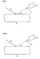
- C 1s electrons and N 1s electrons on the surface of Al x Ga y In 1-x-y N substrate 51 are released as photoelectrons 71.
- photoelectrons 71 released with an angle of 10° relative to the surface of Al x Ga y In 1-x-y N substrate 51 is detected by a detector 81 (detection angle 10°) to obtain the photoelectron spectrum.
- the ratio between a peak area of C 1s electrons and a peak area of N 1s electrons of this photoelectron spectrum is determined.
- the present invention is directed to a cleaning method in which an Al x Ga y In 1-x-y N substrate is soaked in an acid solution, whereby, in a photoelectron spectrum of a surface of the Al x Ga y In 1-x-y N substrate by the X-ray photoelectron spectroscopy with a detection angle of 10°, the ratio between a peak area of C 1s electrons and a peak area of N 1s electrons (C 1s electron peak area / N 1s electron peak area) is made to be at most 3.
- the acid solution is at least one selected from the group consisting of hydrofluoric acid, hydrochloric acid and sulfuric acid. Further preferably, the acid solution is a mixture of at least one selected from the group consisting of hydrofluoric acid, hydrochloric acid and sulfuric acid and a hydrogen peroxide solution.
- the ratio between the peak area of C 1s electrons and the peak area of N 1s electrons in a photoelectron spectrum as above tends to be controlled to be at most 3 more stably.
- the acid solution is made of at least one selected from the group consisting of hydrofluoric acid, hydrochloric acid and sulfuric acid
- the total concentration of hydrofluoric acid, hydrochloric acid and sulfuric acid in the acid solution is at least 0.5 weight percent.
- the acid solution is made of a mixture of at least one selected from the group consisting of hydrofluoric acid, hydrochloric acid and sulfuric acid and a hydrogen peroxide solution
- the total concentration of hydrofluoric acid, hydrochloric acid and sulfuric acid in the acid solution is at least 0.1 weight percent
- the concentration of a hydrogen peroxide solution is at least 0.1 weight percent.
- the ratio between the peak area of C 1s electrons and the peak area of N 1s electrons in a photoelectron spectrum as above tends to be controlled to be at most three further stably.
- the soaking time of the Al x Ga y In 1-x-y N substrate in the acid solution is also at least 30 seconds.
- the ratio between the peak area of C 1s electrons and the peak area of N 1s electrons as above tends to be controlled as above more stably.
- the present invention is directed to an AlN substrate in which, in a photoelectron spectrum of a surface of the AlN substrate by the X-ray photoelectron spectroscopy (XPS) with a detection angle of 10°, the ratio between a peak area of Al 2s electrons and a peak area of N 1s electrons (Al 2s , electron peak area / N 1s electron peak area) is at most 0.65.
- XPS X-ray photoelectron spectroscopy
- an epitaxial film is grown using MOVPE method (Metal Organic Vapor Phase Epitaxial Growth method) or MBE method (Molecular Beam Epitaxy method) on an AlN substrate
- MOVPE method Metal Organic Vapor Phase Epitaxial Growth method
- MBE method Molecular Beam Epitaxy method
- the surface of the AlN substrate is heated before growing the film.
- N (nitrogen) in the surface of the AlN substrate is volatilized more than Al (aluminum) by the heating of the surface of the AlN substrate, much Al is contained in the chemical composition of the surface of the AlN substrate when the epitaxial film is grown. Accordingly, by making the chemical composition of the surface of the AlN substrate to contain much N in advance, an epitaxial film with low haze level can be grown.
- an AlN substrate of which ratio between the peak area of Al 2 s electrons and a peak area of N 1s electrons in a photoelectron spectrum of a surface of the AlN substrate by the X-ray photoelectron spectroscopy (XPS) with a detection angle of 10° is at most 0.65, may be used.
- XPS X-ray photoelectron spectroscopy
- Al 2s electrons refer to electrons of 2s orbit of Al
- N 1s electrons refer to electrons of 1s orbit ofN.
- X-ray 62 by irradiation of X-ray 62, Al 2s electrons and N 1s electrons on the surface of AlN substrate 52 are released as photoelectrons 72. Thereafter, photoelectrons 72 released with an angle of 10° relative to the surface of AlN substrate 52 is detected by a detector 82 (detection angle 10°) to obtain the photoelectron spectrum. The ratio between a peak area of Al 2s electrons and a peak area of N 1s electrons of this photoelectron spectrum is determined.
- the present invention is directed to a cleaning method in which an AlN substrate is soaked in an acid solution, whereby, in a photoelectron spectrum of a surface of the AlN substrate by the X-ray photoelectron spectroscopy with a detection angle of 10°, the ratio between a peak area of Al 2s electrons and a peak area of N 1s electrons (Al 2 , electron peak area / N 1s electron peak area) is made to be at most 0.65
- the acid solution is made of at least one of hydrofluoric acid, hydrochloric acid and sulfuric acid, or a mixture solution made of at least two of these acid.
- the ratio between the peak area of Al 2s electrons and the peak area of N 1s electrons as above tends to be controlled to be at most 0.65 more stably.
- the concentration of the acid solution is at least 0.5 weight percent relative to the whole acid solution.
- the ratio between the peak area of Al 2s electrons and the peak area of N 1s electrons in a photoelectron spectrum as above tends to be controlled to be at most 0.65 further stably.
- the soaking time of the AlN substrate in the acid solution is at least 40 seconds.
- the ratio between the peak area of Al 2s electrons and the peak area of N 1s electrons as above tends to be controlled as above more stably.
- 50 pieces of AlN substrates having a diameter of two inches were prepared, each obtained by mirror-grinding an AlN crystal grown through HVPE method and thereafter removing a damage layer due to the mirror grinding.
- the 50 pieces of AlN substrates each have a thickness of 400 ⁇ m, and the surface of an AlN substrate is a plane 2° off from orientation (0001).
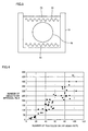
- a cleaning bath 13 shown in Fig. 3 was filled with tetramethylammonium hydroxide aqueous solution in various concentrations as a cleaning solution 23.
- Ultrasound 33 at a frequency of 900 kHz was applied to cleaning solution 23, in which AlN substrates 43 were soaked, with the same condition as to each of 50 pieces of AlN substrates 43.
- the number of particles having a grain size of at least 0.2 ⁇ m on the surface of the AlN substrate was counted with a substrate surface inspection apparatus of the light scattering scheme.
- an epitaxial film formed of an AlN crystal of 1 ⁇ m thickness was grown on the surface of each of the 50 pieces of AlN substrates under the same condition through MOVPE method (Metal Organic Vapor Phase Epitaxial Growth method). Then, with the same substrate surface inspection apparatus as above, the number of defects of the epitaxial films was counted.
- MOVPE method Metal Organic Vapor Phase Epitaxial Growth method
- Fig. 4 shows the result of this experiment.
- the abscissa indicates the number of particles having a grain size of at least 0.2 ⁇ m on the surface of AlN substrate after cleaning counted in a manner described above, while the ordinate indicates the number of defects counted for the epitaxial film grown on the surface of the AlN substrate, corresponding to the number of particles of the abscissa.
- the AlN substrate in which the number of particles having a grain size of at least 0.2 ⁇ m on the surface is at most 20, was the one cleaned with the cleaning solution in which the concentration of tetramethylammonium hydroxide relative to the whole cleaning solution was made to be at least 0.5 weight percent and with the soaking time of at least 30 seconds.
- Example 1 While the AlN substrates were used in Example 1 above, it is considered that the similar result can be obtained when Al x Ga y In 1-x-y N substrates other than the AlN substrates are used. Additionally, the thickness and plane orientation of the AlN substrate are not limited as described above, and a result similar to Example 1 can be obtained with arbitrary values.
- Example 1 50 pieces of AlN substrates having a diameter of two inches were prepared, each obtained by mirror-grinding an AlN crystal and thereafter removing a damage layer due to the mirror grinding.
- the 50 pieces of AlN substrates each have a thickness of 400 ⁇ m, and the surface of an AlN substrate is a plane 2° off from orientation (0001).
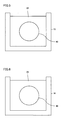
- a cleaning bath 15 shown in Fig. 5 was filled with hydrochloric acid in various concentrations as an acid solution 25 to soak respective AlN substrates 45.
- a photoelectron spectrum of the surface of the AlN substrate was measured by an X-ray photoelectron spectroscopy apparatus employing K ⁇ ray of Mg as X-ray source with a detection angle of 10° to calculate the ratio between a peak area of C 1s electrons and a peak area of N 1s electrons (C 1s electron peak area / N 1s electron peak area).
- the AlN substrate in which the ratio between the peak area of C 1s electrons and the peak area of N 1s electrons (C 1s electron peak area / N 1s electron peak area) was at most 3, was the one cleaned with the cleaning solution in which the concentration of hydrochloric acid relative to the whole cleaning solution was made to be at least 0.5 weight percent and with the soaking time of at least 30 seconds.
- Example 2 While the AlN substrates were used in Example 2 above, it is considered that the similar result can be obtained when Al x Ga y In 1-x-y N substrates other than the AlN substrates are used. Additionally, the thickness and plane orientation of the AlN substrate are not limited as described above, and a result similar as Example 2 can be obtained with arbitrary values.
- 50 pieces of AlN substrates having a diameter of two inches were prepared, each obtained by mirror-grinding an AlN crystal grown through HVPE method and thereafter removing a damage layer due to the mirror grinding.
- the 50 pieces of AlN substrates each have a thickness of 400 ⁇ m, and the surface of an AlN substrate is a plane 2° off from orientation (0001).
- a cleaning bath 16 shown in Fig. 6 was filled with mixture solution of nitric acid, phosphoric acid and acetic acid in various concentrations as a cleaning solution 26 to clean AlN substrates 46 with various different cleaning time periods.
- a photoelectron spectrum of the surface of the AlN substrate was measured by an X-ray photoelectron spectroscopy apparatus employing K ⁇ ray of Mg as X-ray source with a detection angle of 10° to calculate the ratio between a peak area of Al 2s electrons and a peak area of N 1s electrons (Al 2s electron peak area / N 1s electron peak area).
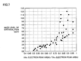
- the abscissa indicates the ratio between a peak area of Al 2s electrons and a peak area of N 1s electrons (Al 2s electron peak area / N 1s electron peak area) of the AlN substrate after cleaning obtained by the X-ray photoelectron spectroscopy apparatus, while the ordinate indicates the haze level of an epitaxial film grown on each AlN substrate having (Al 2s electron peak area / N 1s electron peak area) of the abscissa.
- the AlN substrate in which the ratio between the peak area of Al 2s electrons and the peak area of N 1s electrons (Al 2s electron peak area / N 1s electron peak area) was at most 0.65, was the one cleaned with the acid solution in which the concentration of nitric acid, phosphoric acid and acetic acid relative to the whole cleaning solution was made to be at least 0.5 weight percent and with the soaking time of at least 40 seconds.
- Example 3 While the mixture solution of nitric acid, phosphoric acid and acetic acid was used in Example 3 above, it is considered that the similar result can be obtained when one of nitric acid, phosphoric acid and acetic acid, or a mixture solution made of two of these acid is used.
- the thickness and plane orientation of the AlN substrate are not limited as described above, and a result similar to Example 3 can be obtained with arbitrary values.
- the present invention may suitably be used in the manufacture of a semiconductor device using an Al x Ga y In 1-x-y N substrate. Further, the present invention may suitably be used in the manufacture of a semiconductor device using an AlN substrate is used.
- An Al x Ga y In 1-x-y N substrate wherein particles having a grain size of at least 0.2 ⁇ m on a surface of said Al x Ga y In 1-x-y N substrate are at most 20 in number when a diameter of said Al x Ga y In 1-x-y N substrate is two inches.
- a cleaning method of an Al x Ga y In 1-x-y N substrate (43) wherein said Al x Ga y In 1-x-y N substrate (43) is soaked in a cleaning solution (23) made of one selected from the group consisting of an ammonia water, an ammonia hydroxide/hydrogen peroxide mixture and an organoalkali aqueous solution while being subjected to ultrasound (33), whereby particles having a grain size of at least 0.2 m on a surface of said Al x Ga y In 1-x-y N substrate (43) are made to be at most 20 in number when a diameter of said Al x Ga y In 1-x-y N substrate (43) is two inches.
- a cleaning solution (23) made of one selected from the group consisting of an ammonia water, an ammonia hydroxide/hydrogen peroxide mixture and an organoalkali aqueous solution while being subjected to ultrasound (33), whereby particles having a grain size of at least 0.2 m on a surface of said Al
- the cleaning method of an Al x Ga y In 1-x-y N substrate (43) wherein as said cleaning solution (23), one of an ammonia water having an ammonia concentration of at least 0.5 weight percent, an ammonia hydroxide/hydrogen peroxide mixture having a hydrogen peroxide solution concentration of at least 0.1 weight percent and an ammonia concentration of at least 0.1 weight percent, and an organoalkali aqueous solution having an organoalkali concentration of at least 0.5 weight percent is used.
- an AlN substrate (52) wherein in a photoelectron spectrum of a surface of said AlN substrate (52) by X-ray photoelectron spectroscopy with a detection angle of 10 deg. , a ratio between a peak area of Al 2s electrons and a peak area of N 1s electrons (Al 2s electron peak area / N 1s electron peak area) is at most 0.65.
- a cleaning method of an AlN substrate (46) wherein said AlN substrate (46) is soaked in an acid solution (26), whereby, in a photoelectron spectrum of a surface of said AlN substrate (46) by the X-ray photoelectron spectroscopy with a detection angle of 10 deg. , a ratio between a peak area of Al2s electrons and a peak area of N 1s electrons (Al 2s electron peak area / N 1s electron peak area) is made to be at most 0.65.
Landscapes
- Chemical & Material Sciences (AREA)
- Engineering & Computer Science (AREA)
- Crystallography & Structural Chemistry (AREA)
- Materials Engineering (AREA)
- Metallurgy (AREA)
- Organic Chemistry (AREA)
- Cleaning Or Drying Semiconductors (AREA)
- Crystals, And After-Treatments Of Crystals (AREA)
- Analysing Materials By The Use Of Radiation (AREA)
- Ceramic Products (AREA)
Applications Claiming Priority (3)
| Application Number | Priority Date | Filing Date | Title |
|---|---|---|---|
| JP2004195507A JP4379229B2 (ja) | 2004-07-01 | 2004-07-01 | AlN基板とAlN基板の洗浄方法 |
| JP2004195506A JP2006016249A (ja) | 2004-07-01 | 2004-07-01 | AlxGayIn1−x−yN基板とAlxGayIn1−x−yN基板の洗浄方法 |
| EP05013957.5A EP1612301B1 (fr) | 2004-07-01 | 2005-06-28 | Substrats d'AlN et procédé de nettoyage de substrats d'AlN |
Related Parent Applications (3)
| Application Number | Title | Priority Date | Filing Date |
|---|---|---|---|
| EP05013957.5A Division EP1612301B1 (fr) | 2004-07-01 | 2005-06-28 | Substrats d'AlN et procédé de nettoyage de substrats d'AlN |
| EP05013957.5A Division-Into EP1612301B1 (fr) | 2004-07-01 | 2005-06-28 | Substrats d'AlN et procédé de nettoyage de substrats d'AlN |
| EP05013957.5 Division | 2005-06-28 |
Publications (3)
| Publication Number | Publication Date |
|---|---|
| EP2204478A2 true EP2204478A2 (fr) | 2010-07-07 |
| EP2204478A3 EP2204478A3 (fr) | 2010-08-11 |
| EP2204478B1 EP2204478B1 (fr) | 2014-06-11 |
Family
ID=35134668
Family Applications (3)
| Application Number | Title | Priority Date | Filing Date |
|---|---|---|---|
| EP10003588.0A Ceased EP2204478B1 (fr) | 2004-07-01 | 2005-06-28 | Substrats d'AlN et un procédé de nettoyage de substrats d'AlN |
| EP05013957.5A Ceased EP1612301B1 (fr) | 2004-07-01 | 2005-06-28 | Substrats d'AlN et procédé de nettoyage de substrats d'AlN |
| EP10003590.6A Ceased EP2204479B1 (fr) | 2004-07-01 | 2005-06-28 | Procédé de nettoyage de substrats de AlGaInN et de AlN |
Family Applications After (2)
| Application Number | Title | Priority Date | Filing Date |
|---|---|---|---|
| EP05013957.5A Ceased EP1612301B1 (fr) | 2004-07-01 | 2005-06-28 | Substrats d'AlN et procédé de nettoyage de substrats d'AlN |
| EP10003590.6A Ceased EP2204479B1 (fr) | 2004-07-01 | 2005-06-28 | Procédé de nettoyage de substrats de AlGaInN et de AlN |
Country Status (4)
| Country | Link |
|---|---|
| US (2) | US7387989B2 (fr) |
| EP (3) | EP2204478B1 (fr) |
| KR (2) | KR101188516B1 (fr) |
| TW (1) | TWI408263B (fr) |
Families Citing this family (7)
| Publication number | Priority date | Publication date | Assignee | Title |
|---|---|---|---|---|
| TWI408263B (zh) * | 2004-07-01 | 2013-09-11 | 住友電氣工業股份有限公司 | AlxGayIn1-x-yN基板、AlxGayIn1-x-yN基板之清潔方法、AlN基板及AlN基板之清潔方法 |
| JP2008037705A (ja) * | 2006-08-07 | 2008-02-21 | Sumitomo Electric Ind Ltd | GaxIn1−xN基板とGaxIn1−xN基板の洗浄方法 |
| US8283694B2 (en) | 2006-10-19 | 2012-10-09 | Sumitomo Electric Industries, Ltd. | GaN substrate, epitaxial layer-provided substrate, methods of manufacturing the same, and method of manufacturing semiconductor device |
| WO2008047627A1 (fr) * | 2006-10-19 | 2008-04-24 | Sumitomo Electric Industries, Ltd. | Substrat à base de nitrure d'élément du groupe iii, substrat présentant une couche épitaxiale, procédé de fabrication de ces substrats et procédé de fabrication d'un élément semiconducteur |
| JP2012178458A (ja) | 2011-02-25 | 2012-09-13 | Fujitsu Ltd | 半導体装置の製造方法及び半導体基板の洗浄方法 |
| EP3514266B1 (fr) * | 2017-05-26 | 2025-10-15 | Sumitomo Electric Industries, Ltd. | Substrat semi-conducteur composé du groupe iii-v et substrat semi-conducteur composé du groupe iii-v avec couche épitaxiale |
| WO2023026924A1 (fr) | 2021-08-23 | 2023-03-02 | 株式会社トクヤマ | Procédé de nettoyage et procédé de production de substrat monocristallin de nitrure du groupe iii |
Family Cites Families (16)
| Publication number | Priority date | Publication date | Assignee | Title |
|---|---|---|---|---|
| JPH04126863A (ja) * | 1990-09-12 | 1992-04-27 | Toli Corp Ltd | フックドラグの製造方法 |
| AU7221294A (en) * | 1993-07-30 | 1995-02-28 | Semitool, Inc. | Methods for processing semiconductors to reduce surface particles |
| DE19525521B4 (de) * | 1994-07-15 | 2007-04-26 | Lam Research Corp.(N.D.Ges.D.Staates Delaware), Fremont | Verfahren zum Reinigen von Substraten |
| JPH10233382A (ja) * | 1997-02-17 | 1998-09-02 | Hewlett Packard Co <Hp> | 半導体の表面清浄方法 |
| US6218280B1 (en) * | 1998-06-18 | 2001-04-17 | University Of Florida | Method and apparatus for producing group-III nitrides |
| US6230720B1 (en) * | 1999-08-16 | 2001-05-15 | Memc Electronic Materials, Inc. | Single-operation method of cleaning semiconductors after final polishing |
| JP2001160627A (ja) * | 1999-11-30 | 2001-06-12 | Toyoda Gosei Co Ltd | Iii族窒化物系化合物半導体発光素子 |
| US6447604B1 (en) * | 2000-03-13 | 2002-09-10 | Advanced Technology Materials, Inc. | Method for achieving improved epitaxy quality (surface texture and defect density) on free-standing (aluminum, indium, gallium) nitride ((al,in,ga)n) substrates for opto-electronic and electronic devices |
| JP4126863B2 (ja) * | 2000-10-13 | 2008-07-30 | 松下電器産業株式会社 | 半導体装置の製造方法および半導体基板の製造方法 |
| AU2002219978A1 (en) * | 2000-11-30 | 2002-06-11 | Kyma Technologies, Inc. | Method and apparatus for producing miiin columns and miiin materials grown thereon |
| JP3631724B2 (ja) * | 2001-03-27 | 2005-03-23 | 日本電気株式会社 | Iii族窒化物半導体基板およびその製造方法 |
| US6723165B2 (en) * | 2001-04-13 | 2004-04-20 | Matsushita Electric Industrial Co., Ltd. | Method for fabricating Group III nitride semiconductor substrate |
| JP2003068655A (ja) * | 2001-08-27 | 2003-03-07 | Hoya Corp | 化合物単結晶の製造方法 |
| PL225235B1 (pl) * | 2001-10-26 | 2017-03-31 | Ammono Spółka Z Ograniczoną Odpowiedzialnością | Objętościowy monokryształ azotkowy oraz jego zastosowanie jako podłoże do epitaksji |
| JP2003327497A (ja) * | 2002-05-13 | 2003-11-19 | Sumitomo Electric Ind Ltd | GaN単結晶基板、窒化物系半導体エピタキシャル基板、窒化物系半導体素子及びその製造方法 |
| TWI408263B (zh) * | 2004-07-01 | 2013-09-11 | 住友電氣工業股份有限公司 | AlxGayIn1-x-yN基板、AlxGayIn1-x-yN基板之清潔方法、AlN基板及AlN基板之清潔方法 |
-
2005
- 2005-06-07 TW TW094118827A patent/TWI408263B/zh active
- 2005-06-09 US US11/148,239 patent/US7387989B2/en not_active Expired - Fee Related
- 2005-06-28 EP EP10003588.0A patent/EP2204478B1/fr not_active Ceased
- 2005-06-28 EP EP05013957.5A patent/EP1612301B1/fr not_active Ceased
- 2005-06-28 EP EP10003590.6A patent/EP2204479B1/fr not_active Ceased
- 2005-06-30 KR KR1020050057522A patent/KR101188516B1/ko not_active Expired - Fee Related
-
2008
- 2008-05-08 US US12/149,776 patent/US20080299375A1/en not_active Abandoned
-
2011
- 2011-09-26 KR KR1020110097166A patent/KR101239545B1/ko not_active Expired - Fee Related
Non-Patent Citations (2)
| Title |
|---|
| TOSHIO NISHIDA ET AL.: "GaN-free transparent ultraviolet light-emitting diodes", APPL. PHYS. LETT., vol. 82, no. 1, 2003, XP012033428, DOI: doi:10.1063/1.1533851 |
| TOSHIO NISHIDA ET AL.: "The Characteristics of UV-LED Grown on Bulk AIN Substrate Under Large Current Injection", JAPAN SOCIETY OF APPLIED PHYSICS AND RELATED SOCIETIES, March 2004 (2004-03-01), pages 409 |
Also Published As
| Publication number | Publication date |
|---|---|
| EP1612301A2 (fr) | 2006-01-04 |
| EP2204478B1 (fr) | 2014-06-11 |
| EP2204478A3 (fr) | 2010-08-11 |
| EP1612301A3 (fr) | 2008-12-31 |
| KR20060048731A (ko) | 2006-05-18 |
| TW200610843A (en) | 2006-04-01 |
| EP1612301B1 (fr) | 2014-10-15 |
| EP2204479A3 (fr) | 2010-08-04 |
| US20060003134A1 (en) | 2006-01-05 |
| KR101188516B1 (ko) | 2012-10-05 |
| KR101239545B1 (ko) | 2013-03-06 |
| EP2204479B1 (fr) | 2014-06-25 |
| US20080299375A1 (en) | 2008-12-04 |
| US7387989B2 (en) | 2008-06-17 |
| KR20110120258A (ko) | 2011-11-03 |
| EP2204479A2 (fr) | 2010-07-07 |
| TWI408263B (zh) | 2013-09-11 |
Similar Documents
| Publication | Publication Date | Title |
|---|---|---|
| CN102187020B (zh) | 磷化铟基板的制造方法、外延晶片的制造方法、磷化铟基板及外延晶片 | |
| JP7060060B2 (ja) | エピタキシャル成長用の化合物半導体基板の製造方法、化合物半導体基板上のエピタキシャル成長方法および化合物半導体基板 | |
| Guo et al. | Comparative study of etching high crystalline quality AlN and GaN | |
| US20080299375A1 (en) | ALxGayIn1-x-yN substrate, cleaning method of AIxGayIn1-x-yN substrate, AIN substrate, and cleaning method of AIN substrate | |
| Lin et al. | The dependence of the electrical characteristics of the GaN epitaxial layer on the thermal treatment of the GaN buffer layer | |
| Zhang et al. | Effect of annealing on ZnO thin films grown on (001) silicon substrate by low-pressure metalorganic chemical vapour deposition | |
| EP2154709A2 (fr) | Procédé de fabrication de substrat lié à couche de semi-conducteur de nitrure de groupe III | |
| WO2009142311A1 (fr) | Structure stratifiée de semi-conducteur au nitrure du groupe iii et procédé de fabrication de la structure stratifiée de semi-conducteur au nitrure du groupe iii | |
| US20190257002A1 (en) | GaAs SUBSTRATE AND METHOD FOR MANUFACTURING THE SAME | |
| JP7268461B2 (ja) | ヒ化ガリウム基板、エピタキシャル基板、ヒ化ガリウム基板の製造方法およびエピタキシャル基板の製造方法 | |
| JP2009137776A (ja) | GaAs半導体基板およびその製造方法、ならびにIII−V族化合物半導体デバイスおよびその製造方法 | |
| CN101312164B (zh) | AlxGayIn1-x-yN衬底及其清洗方法,AIN衬底及其清洗方法 | |
| EP4467691A1 (fr) | Substrat monocristallin semi-conducteur de composé du groupe iii-v et procédé de production associé | |
| EP2051288A1 (fr) | SUBSTRAT GaxIn1-xN ET PROCEDE DE NETTOYAGE DE SUBSTRAT GaxIn1-xN | |
| JP4379229B2 (ja) | AlN基板とAlN基板の洗浄方法 | |
| Macht et al. | The direct influence of polarity on structural and electro-optical properties of heteroepitaxial GaN | |
| Horn-von Hoegen et al. | Bi surfactant mediated epitaxy of Ge on Si (111) | |
| Lee et al. | Characteristics of deep levels in As-implanted GaN films | |
| US20020068374A1 (en) | Method for manufacturing gallium nitride compound semiconductor element and gallium nitride compound semiconductor element | |
| Suto et al. | Surface characterization of GaN (0001) grown by liquid phase epitaxy using coaxial impact-collision ion scattering spectroscopy | |
| Kim et al. | Growth and characterization of ZnO film on sapphire by the helicon wave plasma assisted evaporation process | |
| JP2019094239A (ja) | Iii族窒化物単結晶積層体の製造方法及びiii族窒化物単結晶積層体 | |
| KR20170093198A (ko) | 탄화 지르코늄 또는 탄화 하프늄을 포함하는 전도성 층으로부터 연장되는 와이어 엘리먼트를 갖는 전자 장치 |
Legal Events
| Date | Code | Title | Description |
|---|---|---|---|
| PUAI | Public reference made under article 153(3) epc to a published international application that has entered the european phase |
Free format text: ORIGINAL CODE: 0009012 |
|
| 17P | Request for examination filed |
Effective date: 20100331 |
|
| AC | Divisional application: reference to earlier application |
Ref document number: 1612301 Country of ref document: EP Kind code of ref document: P |
|
| AK | Designated contracting states |
Kind code of ref document: A2 Designated state(s): DE FR GB |
|
| PUAL | Search report despatched |
Free format text: ORIGINAL CODE: 0009013 |
|
| AK | Designated contracting states |
Kind code of ref document: A3 Designated state(s): DE FR GB |
|
| RIC1 | Information provided on ipc code assigned before grant |
Ipc: C30B 33/00 20060101AFI20110330BHEP Ipc: H01L 31/00 20060101ALI20110330BHEP Ipc: C30B 29/40 20060101ALI20110330BHEP |
|
| 17Q | First examination report despatched |
Effective date: 20110413 |
|
| GRAP | Despatch of communication of intention to grant a patent |
Free format text: ORIGINAL CODE: EPIDOSNIGR1 |
|
| INTG | Intention to grant announced |
Effective date: 20140218 |
|
| GRAS | Grant fee paid |
Free format text: ORIGINAL CODE: EPIDOSNIGR3 |
|
| GRAA | (expected) grant |
Free format text: ORIGINAL CODE: 0009210 |
|
| AC | Divisional application: reference to earlier application |
Ref document number: 1612301 Country of ref document: EP Kind code of ref document: P |
|
| AK | Designated contracting states |
Kind code of ref document: B1 Designated state(s): DE FR GB |
|
| REG | Reference to a national code |
Ref country code: GB Ref legal event code: FG4D |
|
| REG | Reference to a national code |
Ref country code: DE Ref legal event code: R096 Ref document number: 602005043905 Country of ref document: DE Effective date: 20140724 |
|
| REG | Reference to a national code |
Ref country code: DE Ref legal event code: R097 Ref document number: 602005043905 Country of ref document: DE |
|
| PLBE | No opposition filed within time limit |
Free format text: ORIGINAL CODE: 0009261 |
|
| STAA | Information on the status of an ep patent application or granted ep patent |
Free format text: STATUS: NO OPPOSITION FILED WITHIN TIME LIMIT |
|
| 26N | No opposition filed |
Effective date: 20150312 |
|
| GBPC | Gb: european patent ceased through non-payment of renewal fee |
Effective date: 20140911 |
|
| REG | Reference to a national code |
Ref country code: DE Ref legal event code: R097 Ref document number: 602005043905 Country of ref document: DE Effective date: 20150312 |
|
| PG25 | Lapsed in a contracting state [announced via postgrant information from national office to epo] |
Ref country code: GB Free format text: LAPSE BECAUSE OF NON-PAYMENT OF DUE FEES Effective date: 20140911 |
|
| REG | Reference to a national code |
Ref country code: FR Ref legal event code: PLFP Year of fee payment: 12 |
|
| REG | Reference to a national code |
Ref country code: FR Ref legal event code: PLFP Year of fee payment: 13 |
|
| PGFP | Annual fee paid to national office [announced via postgrant information from national office to epo] |
Ref country code: FR Payment date: 20170511 Year of fee payment: 13 |
|
| PG25 | Lapsed in a contracting state [announced via postgrant information from national office to epo] |
Ref country code: FR Free format text: LAPSE BECAUSE OF NON-PAYMENT OF DUE FEES Effective date: 20180630 |
|
| PGFP | Annual fee paid to national office [announced via postgrant information from national office to epo] |
Ref country code: DE Payment date: 20220505 Year of fee payment: 18 |
|
| REG | Reference to a national code |
Ref country code: DE Ref legal event code: R119 Ref document number: 602005043905 Country of ref document: DE |
|
| PG25 | Lapsed in a contracting state [announced via postgrant information from national office to epo] |
Ref country code: DE Free format text: LAPSE BECAUSE OF NON-PAYMENT OF DUE FEES Effective date: 20240103 |