EP2204818A2 - Activation d'un contrôleur de mémoire intégrée pour travailler de manière transparente avec des dispositifs à mémoire défectueuse - Google Patents
Activation d'un contrôleur de mémoire intégrée pour travailler de manière transparente avec des dispositifs à mémoire défectueuse Download PDFInfo
- Publication number
- EP2204818A2 EP2204818A2 EP09252883A EP09252883A EP2204818A2 EP 2204818 A2 EP2204818 A2 EP 2204818A2 EP 09252883 A EP09252883 A EP 09252883A EP 09252883 A EP09252883 A EP 09252883A EP 2204818 A2 EP2204818 A2 EP 2204818A2
- Authority
- EP
- European Patent Office
- Prior art keywords
- logic
- marginal
- memory module
- memory
- error
- Prior art date
- Legal status (The legal status is an assumption and is not a legal conclusion. Google has not performed a legal analysis and makes no representation as to the accuracy of the status listed.)
- Withdrawn
Links
- 230000002950 deficient Effects 0.000 title abstract description 14
- 238000000034 method Methods 0.000 claims abstract description 23
- 238000012937 correction Methods 0.000 claims description 4
- 238000001514 detection method Methods 0.000 claims description 3
- 230000002085 persistent effect Effects 0.000 claims description 3
- 238000012546 transfer Methods 0.000 claims description 2
- 230000004044 response Effects 0.000 abstract description 3
- 230000007246 mechanism Effects 0.000 abstract description 2
- 238000010586 diagram Methods 0.000 description 8
- 230000008569 process Effects 0.000 description 7
- 230000007547 defect Effects 0.000 description 4
- 230000003287 optical effect Effects 0.000 description 2
- 230000009471 action Effects 0.000 description 1
- 239000000872 buffer Substances 0.000 description 1
- 230000008859 change Effects 0.000 description 1
- 238000004891 communication Methods 0.000 description 1
- 238000004590 computer program Methods 0.000 description 1
- 230000009977 dual effect Effects 0.000 description 1
- 230000006870 function Effects 0.000 description 1
- 230000006872 improvement Effects 0.000 description 1
- 238000004519 manufacturing process Methods 0.000 description 1
- 238000013507 mapping Methods 0.000 description 1
- 238000012545 processing Methods 0.000 description 1
Images


Classifications
-
- G—PHYSICS
- G11—INFORMATION STORAGE
- G11C—STATIC STORES
- G11C29/00—Checking stores for correct operation ; Subsequent repair; Testing stores during standby or offline operation
- G11C29/04—Detection or location of defective memory elements, e.g. cell constructio details, timing of test signals
- G11C29/50—Marginal testing, e.g. race, voltage or current testing
-
- G—PHYSICS
- G11—INFORMATION STORAGE
- G11C—STATIC STORES
- G11C11/00—Digital stores characterised by the use of particular electric or magnetic storage elements; Storage elements therefor
- G11C11/21—Digital stores characterised by the use of particular electric or magnetic storage elements; Storage elements therefor using electric elements
- G11C11/34—Digital stores characterised by the use of particular electric or magnetic storage elements; Storage elements therefor using electric elements using semiconductor devices
- G11C11/40—Digital stores characterised by the use of particular electric or magnetic storage elements; Storage elements therefor using electric elements using semiconductor devices using transistors
- G11C11/401—Digital stores characterised by the use of particular electric or magnetic storage elements; Storage elements therefor using electric elements using semiconductor devices using transistors forming cells needing refreshing or charge regeneration, i.e. dynamic cells
- G11C11/4063—Auxiliary circuits, e.g. for addressing, decoding, driving, writing, sensing or timing
- G11C11/407—Auxiliary circuits, e.g. for addressing, decoding, driving, writing, sensing or timing for memory cells of the field-effect type
- G11C11/4078—Safety or protection circuits, e.g. for preventing inadvertent or unauthorised reading or writing; Status cells; Test cells
-
- G—PHYSICS
- G11—INFORMATION STORAGE
- G11C—STATIC STORES
- G11C11/00—Digital stores characterised by the use of particular electric or magnetic storage elements; Storage elements therefor
- G11C11/21—Digital stores characterised by the use of particular electric or magnetic storage elements; Storage elements therefor using electric elements
- G11C11/34—Digital stores characterised by the use of particular electric or magnetic storage elements; Storage elements therefor using electric elements using semiconductor devices
- G11C11/40—Digital stores characterised by the use of particular electric or magnetic storage elements; Storage elements therefor using electric elements using semiconductor devices using transistors
- G11C11/401—Digital stores characterised by the use of particular electric or magnetic storage elements; Storage elements therefor using electric elements using semiconductor devices using transistors forming cells needing refreshing or charge regeneration, i.e. dynamic cells
- G11C11/4063—Auxiliary circuits, e.g. for addressing, decoding, driving, writing, sensing or timing
-
- G—PHYSICS
- G11—INFORMATION STORAGE
- G11C—STATIC STORES
- G11C11/00—Digital stores characterised by the use of particular electric or magnetic storage elements; Storage elements therefor
- G11C11/21—Digital stores characterised by the use of particular electric or magnetic storage elements; Storage elements therefor using electric elements
- G11C11/34—Digital stores characterised by the use of particular electric or magnetic storage elements; Storage elements therefor using electric elements using semiconductor devices
- G11C11/40—Digital stores characterised by the use of particular electric or magnetic storage elements; Storage elements therefor using electric elements using semiconductor devices using transistors
- G11C11/401—Digital stores characterised by the use of particular electric or magnetic storage elements; Storage elements therefor using electric elements using semiconductor devices using transistors forming cells needing refreshing or charge regeneration, i.e. dynamic cells
- G11C11/4063—Auxiliary circuits, e.g. for addressing, decoding, driving, writing, sensing or timing
- G11C11/407—Auxiliary circuits, e.g. for addressing, decoding, driving, writing, sensing or timing for memory cells of the field-effect type
- G11C11/4074—Power supply or voltage generation circuits, e.g. bias voltage generators, substrate voltage generators, back-up power, power control circuits
-
- G—PHYSICS
- G11—INFORMATION STORAGE
- G11C—STATIC STORES
- G11C29/00—Checking stores for correct operation ; Subsequent repair; Testing stores during standby or offline operation
- G11C29/02—Detection or location of defective auxiliary circuits, e.g. defective refresh counters
- G11C29/028—Detection or location of defective auxiliary circuits, e.g. defective refresh counters with adaption or trimming of parameters
-
- G—PHYSICS
- G11—INFORMATION STORAGE
- G11C—STATIC STORES
- G11C29/00—Checking stores for correct operation ; Subsequent repair; Testing stores during standby or offline operation
- G11C29/04—Detection or location of defective memory elements, e.g. cell constructio details, timing of test signals
- G11C29/08—Functional testing, e.g. testing during refresh, power-on self testing [POST] or distributed testing
- G11C29/12—Built-in arrangements for testing, e.g. built-in self testing [BIST] or interconnection details
- G11C29/46—Test trigger logic
-
- G—PHYSICS
- G11—INFORMATION STORAGE
- G11C—STATIC STORES
- G11C29/00—Checking stores for correct operation ; Subsequent repair; Testing stores during standby or offline operation
- G11C29/04—Detection or location of defective memory elements, e.g. cell constructio details, timing of test signals
- G11C29/50—Marginal testing, e.g. race, voltage or current testing
- G11C29/50016—Marginal testing, e.g. race, voltage or current testing of retention
-
- G—PHYSICS
- G11—INFORMATION STORAGE
- G11C—STATIC STORES
- G11C29/00—Checking stores for correct operation ; Subsequent repair; Testing stores during standby or offline operation
- G11C29/70—Masking faults in memories by using spares or by reconfiguring
- G11C29/76—Masking faults in memories by using spares or by reconfiguring using address translation or modifications
-
- G—PHYSICS
- G11—INFORMATION STORAGE
- G11C—STATIC STORES
- G11C29/00—Checking stores for correct operation ; Subsequent repair; Testing stores during standby or offline operation
- G11C29/04—Detection or location of defective memory elements, e.g. cell constructio details, timing of test signals
- G11C2029/0409—Online test
-
- G—PHYSICS
- G11—INFORMATION STORAGE
- G11C—STATIC STORES
- G11C29/00—Checking stores for correct operation ; Subsequent repair; Testing stores during standby or offline operation
- G11C29/04—Detection or location of defective memory elements, e.g. cell constructio details, timing of test signals
- G11C2029/0411—Online error correction
-
- G—PHYSICS
- G11—INFORMATION STORAGE
- G11C—STATIC STORES
- G11C29/00—Checking stores for correct operation ; Subsequent repair; Testing stores during standby or offline operation
- G11C29/04—Detection or location of defective memory elements, e.g. cell constructio details, timing of test signals
- G11C29/50—Marginal testing, e.g. race, voltage or current testing
- G11C2029/5002—Characteristic
-
- G—PHYSICS
- G11—INFORMATION STORAGE
- G11C—STATIC STORES
- G11C29/00—Checking stores for correct operation ; Subsequent repair; Testing stores during standby or offline operation
- G11C29/04—Detection or location of defective memory elements, e.g. cell constructio details, timing of test signals
- G11C29/50—Marginal testing, e.g. race, voltage or current testing
- G11C2029/5004—Voltage
-
- G—PHYSICS
- G11—INFORMATION STORAGE
- G11C—STATIC STORES
- G11C29/00—Checking stores for correct operation ; Subsequent repair; Testing stores during standby or offline operation
- G11C29/56—External testing equipment for static stores, e.g. automatic test equipment [ATE]; Interfaces therefor
- G11C2029/5606—Error catch memory
-
- G—PHYSICS
- G11—INFORMATION STORAGE
- G11C—STATIC STORES
- G11C5/00—Details of stores covered by group G11C11/00
- G11C5/02—Disposition of storage elements, e.g. in the form of a matrix array
- G11C5/04—Supports for storage elements, e.g. memory modules; Mounting or fixing of storage elements on such supports
Definitions
- Embodiments of the invention generally relate to the field of integrated circuits and, more particularly, to systems, methods and apparatuses for enabling an integrated memory controller to transparently work with defective memory devices.
- DRAMs dynamic random access memory devices
- the number of DRAMs on a memory module has also been growing at a substantial rate. All of these manufactured components are subject to the same statistical yield patterns, and this means that as the DRAM density increases there is a corresponding increase in the risk of defective bits in the manufactured components. Current yields for DRAMs are around 90%. The components with defective bits are binned and sold as lower density chips if possible.
- the ever increasing memory footprint of computer operating systems and data processing needs continues to drive the need for larger memory subsystems in computing systems. In almost all segments the memory subsystem cost is becoming a significant part of the total cost of a computing system.
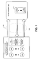
- Figure 1 is a high-level block diagram illustrating selected aspects of a computing system implemented according to an embodiment of the invention.
- Figure 2 is a block diagram illustrating selected aspects of logic to impose a marginal condition on a memory module and to compensate for the imposed marginal condition.
- Figure 3 is a flow diagram illustrating selected aspects of a method for operating a memory module according to an embodiment of the invention.
- Figures 4 is a flow diagram illustrating selected aspects of a method for compensating for a marginal condition imposed on a memory module according to an embodiment of the invention.
- Embodiments of the invention are generally directed to systems, methods, and apparatuses for enabling an integrated memory controller to transparently work with defective memory devices.
- a marginal condition is imposed on a memory module during normal operations of the memory module.
- the term "marginal condition" refers to a condition that is out of compliance with a specified (or "normal") operating condition for the memory module.
- the memory module may exhibit failures in response to the marginal conditions and compensating mechanisms may mitigate the failures.
- FIG. 1 is a high-level block diagram illustrating selected aspects of a computing system implemented according to an embodiment of the invention.
- System 100 includes integrated circuit 102, DRAM subsystem 104, and memory interconnect 106. In alternative embodiments, system 100 may include more elements, fewer elements, and/or different elements.
- Integrated circuit 102 includes logic to control the transfer of information with DRAM subsystem 104.
- integrated circuit 102 includes processor cores 108 and logic 110.
- Processor cores 108 may be any of a wide range of processor cores including general processor cores, graphics processor cores, and the like.
- Logic 110 broadly represents a wide array of logic including, for example, a memory controller, an uncore, and the like.
- logic 110 also includes logic to impose a marginal condition on a memory module (or on another element of DRAM subsystem 104) and logic to compensate for the imposed marginal condition.
- the term "marginal condition” broadly refers to a condition that exceeds the bounds of normal operating conditions as defined by a (public or proprietary) specification, standard, protocol, and the like. For example, normal operating conditions for voltage, temperature, and refresh rate are typically defined for a memory module in a specification or standard.
- the phrase "imposing a marginal condition” refers to operating the device (e.g., the memory module) outside of the range of values that are considered "normal” for the device.
- "imposing a marginal condition” refers to imposing a voltage, a temperature, and/or a refresh rate that is outside of values that are considered "normal” (e.g., as defined by a specification, a standard, or the like).
- logic 110 imposes a refresh rate that is lower than the refresh rate specified for memory module 112.
- the advantages to imposing a lower refresh rate include an improvement in overall system performance since the system is spending less time with its memory in refresh.
- the power consumed by DRAM subsystem 104 may be reduced by reducing the refresh rate.
- operating under lower voltage can yield power savings.
- logic 110 may impose a different marginal condition on memory module 112 (and/or any other element of DRAM subsystem 104 and/or on interconnect 106).
- the phrase "compensating for the imposed marginal condition" refers to detecting a change in the performance of DRAM subsystem 104 and/or compensating for those changes.
- logic 110 imposes a reduced refresh rate on memory module 112. Some of the memory locations in module 112 may exhibit defects in response to the reduced refresh rate. Logic 110 may detect those defects and compensate for them. For example, in some embodiments, logic 110 may move information that is stored in the "defective" memory locations to another location (e.g., one that is known to be operating properly). Aspects of logic 110 are further discussed below with reference to FIGs. 2-4 .
- DRAM subsystem 104 provides at least a portion of the main memory for system 100.
- DRAM subsystem 104 includes one or more memory modules 112.
- Modules 112 may be any of a wide range of memory modules including dual inline memory modules (DIMMs), small outline DIMMs (SO-DIMMs), and the like.
- Each module 112 may have one or more DRAMs 114 (and possibly other elements such as registers, buffers, and the like).
- DRAMs 114 may be any of a wide range of devices including nearly any generation of double data rate (DDR) DRAMs.
- DDR double data rate
- FIG. 1 shows an integrated memory controller (e.g., integrated with the processor). It is to be appreciated, however, that in some embodiments the memory controller may be part of the chipset for computing system 100. In such embodiments, the logic to impose marginal conditions and the logic to compensate for marginal conditions may also be part of the computing system.
- the memory controller may be part of the chipset for computing system 100.
- the logic to impose marginal conditions and the logic to compensate for marginal conditions may also be part of the computing system.
- FIG. 2 is a block diagram illustrating selected aspects of logic to impose a marginal condition on a memory module and logic to compensate for the imposed marginal condition.
- integrated circuit 200 includes marginal condition logic 201, error correction code (ECC) 202, hard error detect logic 204, relocation logic 206, and memory map 208.
- ECC error correction code
- integrated circuit 200 may include more elements, fewer elements, and/or different elements.
- Marginal condition logic 201 includes logic to impose a marginal condition on one or more elements of a DRAM subsystem (e.g., DRAM subsystem 204 shown in FIG. 2 ). In some embodiments, logic 201 includes logic to operate one or more memory modules at a reduced refresh rate. In other embodiments, logic 201 includes logic to impose a marginal voltage and/or a marginal temperature on the memory subsystem. In yet other embodiments, logic 201 may impose a different marginal condition on one or more elements of the DRAM subsystem.
- ECC logic 202 includes logic to detect and correct selected errors in information (e.g., data and/or code) that is read from the DRAM subsystem (e.g., DRAM subsystem 104, shown in FIG. 1 ).
- ECC logic 202 may be coupled with (selected portions) of the memory interconnect (e.g., interconnect 106, shown in FIG. 1 ).
- ECC 202 checks for errors in the data.
- ECC 202 may use any of a wide range of algorithms to check the data (e.g., parity, single error correct - double error detect (SECDEC), Chipkill, and the like). In some embodiments, if ECC 202 detects an error, then it forwards information about the error to logic 204.
- SECDEC single error correct - double error detect
- hard error detect logic 204 determines whether a detected error is a hard error or a soft error.
- the term "soft error” refers to an error in stored information that is not the result of a hardware defect (e.g., an error due to an alpha strike).
- a "hard error” refers to an error that is due to a hardware defect. For example, bits that go bad due to a memory module operating in a marginal condition are hard errors.
- logic 204 determines whether there are hard errors based on whether the error is persistent. For example, logic 204 may use replay logic to write to and read from a memory location a number of times to determine whether one or more bits are persistently bad. The replay logic may be preexisting replay logic (e.g., in a memory controller) or it may replay logic that is part of logic 204.
- relocation logic 206 moves the information stored in the defective memory location to another memory location (e.g., a reserved memory location that is operating normally).
- the term "relocation" refers to moving information from a defective region to a known good region. Relocation may also include building and using memory map 208.
- the process flow for relocation may include changing a pointer, changing a table entry, and the like.
- Memory map 208 is a logical structure that provides a mapping to relocated information and/or provides an indication of which memory locations are currently defective. Memory map 208 may be built and used during the normal operation of a system (e.g., during real time rather than manufacture time). As defective locations are identified and information is relocated, logic 206 builds and uses memory map 208. Relocation is performed before the "hard" error leads to a system failure or data corruption.
- At least a portion of the logic to compensate for the marginal condition is, optionally, performed in software.
- software 210 is a handler such as a system management interrupt handler (e.g., an SMI handler).
- software 210 may be part of the operating system (OS) kernel.
- OS operating system
- FIG. 3 is a flow diagram illustrating selected aspects of a method for operating a memory module according to an embodiment of the invention.
- the process flow illustrated in FIG. 3 may be performed by a computing system such as system 100 illustrated in FIG. 1 .
- the computing system is initialized.
- the term "initialization” refers to, for example, booting, rebooting, starting, powering-up and the like.
- Marginal condition logic imposes a marginal condition at 304.
- the marginal condition is a reduced refresh rate.
- the marginal condition is a marginal operating voltage and/or a marginal temperature.
- the marginal condition may be nearly any other condition that is in variance with the "normal" operating conditions for the DRAM subsystem.
- compensating for the marginal condition includes detecting hard errors and relocating information to a known good memory location.
- the compensating logic uses a memory map to reference the new locations for the relocated data.
- FIG. 4 is a flow diagram illustrating selected aspects of a method for detecting and compensating for a marginal condition imposed on a memory module according to an embodiment of the invention.
- the process shown in FIG. 4 is performed by hardware (e.g., by elements of integrated circuit 200, shown in FIG. 2 ).
- the process (or portions of the process) may be performed by software (e.g., software 210, shown in FIG. 2 ).
- an ECC code detects an error in information read from a memory module.
- the ECC code may use any of a wide range of algorithms including parity, SECDED, Chipkill, and the like. If the ECC code detects an error, hard error detection logic determines whether the detected error is a hard error or a soft error at 404. In some embodiments, an error is a considered a hard error if it is persistent. If the hard error detection logic determines that the error is not a hard error, then the error is processed by the ECC code in the conventional manner as shown by 406.
- relocation logic may move the data currently located in the "defective" memory location to a known good location (408).
- the relocation logic may reserve one or more "spare" memory locations (e.g., rows, portions of rows, ranks, and the like) that are functioning normally.
- the information in the defective memory locations may be moved to one of the spare locations.
- the relocation logic uses a memory map to reference the new locations for the relocated data and to indicate where the defective locations are.
- Elements of embodiments of the present invention may also be provided as a machine-readable medium for storing the machine-executable instructions.
- the machine-readable medium may include, but is not limited to, flash memory, optical disks, compact disks-read only memory (CD-ROM), digital versatile/video disks (DVD) ROM, random access memory (RAM), erasable programmable read-only memory (EPROM), electrically erasable programmable read-only memory (EEPROM), magnetic or optical cards, propagation media or other type of machine-readable media suitable for storing electronic instructions.
- embodiments of the invention may be downloaded as a computer program which may be transferred from a remote computer (e.g., a server) to a requesting computer (e.g., a client) by way of data signals embodied in a carrier wave or other propagation medium via a communication link (e.g., a modem or network connection).
- a remote computer e.g., a server
- a requesting computer e.g., a client
- a communication link e.g., a modem or network connection
- logic is representative of hardware, firmware, software (or any combination thereof) to perform one or more functions.
- examples of “hardware” include, but are not limited to, an integrated circuit, a finite state machine, or even combinatorial logic.
- the integrated circuit may take the form of a processor such as a microprocessor, an application specific integrated circuit, a digital signal processor, a micro-controller, or the like.
Landscapes
- Engineering & Computer Science (AREA)
- Microelectronics & Electronic Packaging (AREA)
- Computer Hardware Design (AREA)
- Computer Security & Cryptography (AREA)
- Techniques For Improving Reliability Of Storages (AREA)
- For Increasing The Reliability Of Semiconductor Memories (AREA)
Applications Claiming Priority (1)
| Application Number | Priority Date | Filing Date | Title |
|---|---|---|---|
| US12/345,948 US20100169729A1 (en) | 2008-12-30 | 2008-12-30 | Enabling an integrated memory controller to transparently work with defective memory devices |
Publications (2)
| Publication Number | Publication Date |
|---|---|
| EP2204818A2 true EP2204818A2 (fr) | 2010-07-07 |
| EP2204818A3 EP2204818A3 (fr) | 2010-10-06 |
Family
ID=42115417
Family Applications (1)
| Application Number | Title | Priority Date | Filing Date |
|---|---|---|---|
| EP09252883A Withdrawn EP2204818A3 (fr) | 2008-12-30 | 2009-12-22 | Activation d'un contrôleur de mémoire intégrée pour travailler de manière transparente avec des dispositifs à mémoire défectueuse |
Country Status (4)
| Country | Link |
|---|---|
| US (1) | US20100169729A1 (fr) |
| EP (1) | EP2204818A3 (fr) |
| KR (1) | KR101141487B1 (fr) |
| CN (1) | CN102117236A (fr) |
Families Citing this family (10)
| Publication number | Priority date | Publication date | Assignee | Title |
|---|---|---|---|---|
| US7984250B2 (en) * | 2008-12-31 | 2011-07-19 | Intel Corporation | Dynamic updating of thresholds in accordance with operating conditons |
| TW201302793A (zh) | 2010-09-03 | 2013-01-16 | Glaxo Group Ltd | 新穎之抗原結合蛋白 |
| US9786356B2 (en) * | 2015-01-30 | 2017-10-10 | Qualcomm Incorporated | Memory device with adaptive voltage scaling based on error information |
| EP3453022B1 (fr) | 2016-05-02 | 2022-07-06 | INTEL Corporation | Détection et correction d'erreur (ecc) interne avec des bits de système supplémentaires |
| CN107516547A (zh) * | 2016-06-16 | 2017-12-26 | 中兴通讯股份有限公司 | 内存硬错误的处理方法及装置 |
| US10120749B2 (en) | 2016-09-30 | 2018-11-06 | Intel Corporation | Extended application of error checking and correction code in memory |
| KR102387195B1 (ko) | 2017-11-30 | 2022-04-18 | 에스케이하이닉스 주식회사 | 메모리 시스템 및 이의 에러 정정 방법 |
| US11656938B2 (en) * | 2020-09-28 | 2023-05-23 | Micron Technology, Inc. | Preemptive read verification after hardware write back |
| EP4443300A4 (fr) | 2022-02-21 | 2025-04-16 | Samsung Electronics Co., Ltd. | Dispositif électronique et procédé de commande de celui-ci |
| US20240311222A1 (en) * | 2023-03-13 | 2024-09-19 | International Business Machines Corporation | Computer memory hardware correction using baseline wander |
Family Cites Families (23)
| Publication number | Priority date | Publication date | Assignee | Title |
|---|---|---|---|---|
| JPH09244770A (ja) * | 1996-03-11 | 1997-09-19 | Ricoh Co Ltd | 電子機器の電圧低下制御装置 |
| US5870614A (en) * | 1996-09-25 | 1999-02-09 | Philips Electronics North America Corporation | Thermostat controls dsp's temperature by effectuating the dsp switching between tasks of different compute-intensity |
| US5956350A (en) * | 1997-10-27 | 1999-09-21 | Lsi Logic Corporation | Built in self repair for DRAMs using on-chip temperature sensing and heating |
| JPH11144494A (ja) * | 1997-11-12 | 1999-05-28 | Nec Corp | 半導体メモリ |
| US6351827B1 (en) * | 1998-04-08 | 2002-02-26 | Kingston Technology Co. | Voltage and clock margin testing of memory-modules using an adapter board mounted to a PC motherboard |
| US6085334A (en) * | 1998-04-17 | 2000-07-04 | Motorola, Inc. | Method and apparatus for testing an integrated memory device |
| US6005824A (en) * | 1998-06-30 | 1999-12-21 | Lsi Logic Corporation | Inherently compensated clocking circuit for dynamic random access memory |
| US6415388B1 (en) * | 1998-10-30 | 2002-07-02 | Intel Corporation | Method and apparatus for power throttling in a microprocessor using a closed loop feedback system |
| US6467048B1 (en) * | 1999-10-07 | 2002-10-15 | Compaq Information Technologies Group, L.P. | Apparatus, method and system for using cache memory as fail-over memory |
| US6574763B1 (en) * | 1999-12-28 | 2003-06-03 | International Business Machines Corporation | Method and apparatus for semiconductor integrated circuit testing and burn-in |
| JP2001208798A (ja) * | 2000-01-26 | 2001-08-03 | Mitsubishi Electric Corp | 半導体回路のテスト方法および装置 |
| US6973605B1 (en) * | 2001-06-15 | 2005-12-06 | Artisan Components, Inc. | System and method for assured built in self repair of memories |
| US7260758B1 (en) * | 2001-09-07 | 2007-08-21 | Lsi Corporation | Method and system for performing built-in self-test routines using an accumulator to store fault information |
| US6754117B2 (en) * | 2002-08-16 | 2004-06-22 | Micron Technology, Inc. | System and method for self-testing and repair of memory modules |
| US20040215912A1 (en) * | 2003-04-24 | 2004-10-28 | George Vergis | Method and apparatus to establish, report and adjust system memory usage |
| US7099221B2 (en) * | 2004-05-06 | 2006-08-29 | Micron Technology, Inc. | Memory controller method and system compensating for memory cell data losses |
| US7272758B2 (en) * | 2004-08-31 | 2007-09-18 | Micron Technology, Inc. | Defective memory block identification in a memory device |
| US7424663B2 (en) * | 2005-01-19 | 2008-09-09 | Intel Corporation | Lowering voltage for cache memory operation |
| JP4846383B2 (ja) * | 2006-02-10 | 2011-12-28 | 株式会社日立製作所 | 情報処理装置 |
| US8020038B2 (en) * | 2006-09-28 | 2011-09-13 | Hewlett-Packard Development Company, L.P. | System and method for adjusting operating points of a processor based on detected processor errors |
| JP4939234B2 (ja) * | 2007-01-11 | 2012-05-23 | 株式会社日立製作所 | フラッシュメモリモジュール、そのフラッシュメモリモジュールを記録媒体として用いたストレージ装置及びそのフラッシュメモリモジュールのアドレス変換テーブル検証方法 |
| US7483325B2 (en) * | 2007-03-20 | 2009-01-27 | International Business Machines Corporation | Retention-time control and error management in a cache system comprising dynamic storage |
| US8078918B2 (en) * | 2008-02-07 | 2011-12-13 | Siliconsystems, Inc. | Solid state storage subsystem that maintains and provides access to data reflective of a failure risk |
-
2008
- 2008-12-30 US US12/345,948 patent/US20100169729A1/en not_active Abandoned
-
2009
- 2009-12-22 EP EP09252883A patent/EP2204818A3/fr not_active Withdrawn
- 2009-12-23 KR KR1020090129726A patent/KR101141487B1/ko not_active Expired - Fee Related
- 2009-12-28 CN CN200910215285XA patent/CN102117236A/zh active Pending
Non-Patent Citations (1)
| Title |
|---|
| None |
Also Published As
| Publication number | Publication date |
|---|---|
| CN102117236A (zh) | 2011-07-06 |
| EP2204818A3 (fr) | 2010-10-06 |
| KR101141487B1 (ko) | 2012-07-02 |
| KR20100080383A (ko) | 2010-07-08 |
| US20100169729A1 (en) | 2010-07-01 |
Similar Documents
| Publication | Publication Date | Title |
|---|---|---|
| EP2204818A2 (fr) | Activation d'un contrôleur de mémoire intégrée pour travailler de manière transparente avec des dispositifs à mémoire défectueuse | |
| EP2266116B1 (fr) | Systèmes, procédés et appareils permettant une économie d énergie lors d un autorafraîchissement de la mémoire | |
| EP3132449B1 (fr) | Procédé, appareil et système de traitement d'événements d'erreur de données avec un dispositif de commande de mémoire | |
| US8020053B2 (en) | On-line memory testing | |
| CN108074595B (zh) | 存储器系统的接口方法、接口电路和存储器模块 | |
| US8473791B2 (en) | Redundant memory to mask DRAM failures | |
| US7107493B2 (en) | System and method for testing for memory errors in a computer system | |
| US20070234182A1 (en) | Error checking and correction (ECC) system and method | |
| US11797369B2 (en) | Error reporting for non-volatile memory modules | |
| US11481294B2 (en) | Runtime cell row replacement in a memory | |
| WO2022151717A1 (fr) | Procédé et appareil de réparation de mémoire après encapsulation, support de stockage et dispositif électronique | |
| EP3699747A1 (fr) | Mise à jour de micrologiciel de disque dur à raid | |
| US11282584B2 (en) | Multi-chip package and method of testing the same | |
| JP2008262325A (ja) | メモリ制御装置、メモリ制御方法、情報処理システム、そのプログラム及び記憶媒体 | |
| CN103389921A (zh) | 信号处理电路以及使用了该信号处理电路的试验装置 | |
| US11531585B2 (en) | Memory module and operating method | |
| US11182231B2 (en) | Host system and computing system including the host system | |
| CN104704572A (zh) | 修复内存装置 | |
| KR102427323B1 (ko) | 반도체 메모리 모듈, 반도체 메모리 시스템, 그리고 반도체 메모리 모듈을 액세스하는 액세스 방법 | |
| JP2005078632A (ja) | メモリをテストするシステムおよび方法 | |
| CN116340049A (zh) | 存储器系统及操作存储器系统的方法 | |
| CN120877803A (zh) | 一种参考电阻动态调整方法、装置、设备及可读存储介质 | |
| CN121789743A (zh) | 计算机系统、修复存储器模块的方法以及计算机程序产品 | |
| HK1096473B (en) | Semiconductor device and processing method for starting the same |
Legal Events
| Date | Code | Title | Description |
|---|---|---|---|
| PUAI | Public reference made under article 153(3) epc to a published international application that has entered the european phase |
Free format text: ORIGINAL CODE: 0009012 |
|
| 17P | Request for examination filed |
Effective date: 20100118 |
|
| AK | Designated contracting states |
Kind code of ref document: A2 Designated state(s): AT BE BG CH CY CZ DE DK EE ES FI FR GB GR HR HU IE IS IT LI LT LU LV MC MK MT NL NO PL PT RO SE SI SK SM TR |
|
| AX | Request for extension of the european patent |
Extension state: AL BA RS |
|
| PUAL | Search report despatched |
Free format text: ORIGINAL CODE: 0009013 |
|
| AK | Designated contracting states |
Kind code of ref document: A3 Designated state(s): AT BE BG CH CY CZ DE DK EE ES FI FR GB GR HR HU IE IS IT LI LT LU LV MC MK MT NL NO PL PT RO SE SI SK SM TR |
|
| AX | Request for extension of the european patent |
Extension state: AL BA RS |
|
| 17Q | First examination report despatched |
Effective date: 20101001 |
|
| STAA | Information on the status of an ep patent application or granted ep patent |
Free format text: STATUS: THE APPLICATION IS DEEMED TO BE WITHDRAWN |
|
| 18D | Application deemed to be withdrawn |
Effective date: 20140701 |