EP2204837B1 - Verfahren zur Herstellung eines Schutzfilters gegen elektromagnetische Interferenzen (EMI) für Plasmaanzeigetafel und EMI-Schutzfilter für Plasmaanzeigetafel damit - Google Patents
Verfahren zur Herstellung eines Schutzfilters gegen elektromagnetische Interferenzen (EMI) für Plasmaanzeigetafel und EMI-Schutzfilter für Plasmaanzeigetafel damit Download PDFInfo
- Publication number
- EP2204837B1 EP2204837B1 EP20090179403 EP09179403A EP2204837B1 EP 2204837 B1 EP2204837 B1 EP 2204837B1 EP 20090179403 EP20090179403 EP 20090179403 EP 09179403 A EP09179403 A EP 09179403A EP 2204837 B1 EP2204837 B1 EP 2204837B1
- Authority
- EP
- European Patent Office
- Prior art keywords
- plasma display
- conductive
- display panel
- ink
- mesh pattern
- Prior art date
- Legal status (The legal status is an assumption and is not a legal conclusion. Google has not performed a legal analysis and makes no representation as to the accuracy of the status listed.)
- Active
Links
Images



Classifications
-
- H—ELECTRICITY
- H01—ELECTRIC ELEMENTS
- H01J—ELECTRIC DISCHARGE TUBES OR DISCHARGE LAMPS
- H01J11/00—Gas-filled discharge tubes with alternating current induction of the discharge, e.g. alternating current plasma display panels [AC-PDP]; Gas-filled discharge tubes without any main electrode inside the vessel; Gas-filled discharge tubes with at least one main electrode outside the vessel
- H01J11/20—Constructional details
- H01J11/34—Vessels, containers or parts thereof, e.g. substrates
- H01J11/44—Optical arrangements or shielding arrangements, e.g. filters, black matrices, light reflecting means or electromagnetic shielding means
-
- H—ELECTRICITY
- H01—ELECTRIC ELEMENTS
- H01J—ELECTRIC DISCHARGE TUBES OR DISCHARGE LAMPS
- H01J11/00—Gas-filled discharge tubes with alternating current induction of the discharge, e.g. alternating current plasma display panels [AC-PDP]; Gas-filled discharge tubes without any main electrode inside the vessel; Gas-filled discharge tubes with at least one main electrode outside the vessel
- H01J11/10—AC-PDPs with at least one main electrode being out of contact with the plasma
-
- H—ELECTRICITY
- H01—ELECTRIC ELEMENTS
- H01J—ELECTRIC DISCHARGE TUBES OR DISCHARGE LAMPS
- H01J9/00—Apparatus or processes specially adapted for the manufacture, installation, removal, maintenance of electric discharge tubes, discharge lamps, or parts thereof; Recovery of material from discharge tubes or lamps
- H01J9/20—Manufacture of screens on or from which an image or pattern is formed, picked up, converted or stored; Applying coatings to the vessel
- H01J9/205—Applying optical coatings or shielding coatings to the vessel of flat panel displays, e.g. applying filter layers, electromagnetic interference shielding layers, anti-reflection coatings or anti-glare coatings
-
- H—ELECTRICITY
- H05—ELECTRIC TECHNIQUES NOT OTHERWISE PROVIDED FOR
- H05K—PRINTED CIRCUITS; CASINGS OR CONSTRUCTIONAL DETAILS OF ELECTRIC APPARATUS; MANUFACTURE OF ASSEMBLAGES OF ELECTRICAL COMPONENTS
- H05K9/00—Screening of apparatus or components against electric or magnetic fields
- H05K9/0073—Shielding materials
- H05K9/0094—Shielding materials being light-transmitting, e.g. transparent, translucent
- H05K9/0096—Shielding materials being light-transmitting, e.g. transparent, translucent for television displays, e.g. plasma display panel
-
- H—ELECTRICITY
- H01—ELECTRIC ELEMENTS
- H01J—ELECTRIC DISCHARGE TUBES OR DISCHARGE LAMPS
- H01J2211/00—Plasma display panels with alternate current induction of the discharge, e.g. AC-PDPs
- H01J2211/20—Constructional details
- H01J2211/34—Vessels, containers or parts thereof, e.g. substrates
- H01J2211/44—Optical arrangements or shielding arrangements, e.g. filters or lenses
- H01J2211/446—Electromagnetic shielding means; Antistatic means
-
- Y—GENERAL TAGGING OF NEW TECHNOLOGICAL DEVELOPMENTS; GENERAL TAGGING OF CROSS-SECTIONAL TECHNOLOGIES SPANNING OVER SEVERAL SECTIONS OF THE IPC; TECHNICAL SUBJECTS COVERED BY FORMER USPC CROSS-REFERENCE ART COLLECTIONS [XRACs] AND DIGESTS
- Y10—TECHNICAL SUBJECTS COVERED BY FORMER USPC
- Y10T—TECHNICAL SUBJECTS COVERED BY FORMER US CLASSIFICATION
- Y10T428/00—Stock material or miscellaneous articles
- Y10T428/31504—Composite [nonstructural laminate]
- Y10T428/31551—Of polyamidoester [polyurethane, polyisocyanate, polycarbamate, etc.]
- Y10T428/31645—Next to addition polymer from unsaturated monomers
Definitions
- An aspect of the present invention relates to a method of manufacturing an electromagnetic interference (EMI) shielding filter for a plasma display panel and an plasma display panel using the same.
- EMI electromagnetic interference
- a plasma display device often indudes a plasma display panel having a discharge cell defined by an address electrode, a scan electrode and a sustain electrode, and phosphors being applied to the discharge cell; and a drive unit for driving the plasma display panel.
- the plasma display device displays images through the generation of visible rays in response to excitation of phosphors by the action of ultraviolet rays generated upon gas discharge.
- Plasma display devices often suffer from high-level generation of electromagnetic waves in the plasma display panel during a driving process thereof. For this reason, a plasma display device may be fabricated with a separate electromagnetic interference (EMI) shielding filter for blocking electromagnetic waves to the front or display side of the plasma display panel.
- EMI electromagnetic interference
- the EMI shielding filter is fabricated by the formation of a transparent conductive layer on a separate base such as film or glass substrate.
- a transparent conductive layer and separate base such as film or glass substrate increase production costs of plasma display devices.
- An example of a method of manufacturing an EMI shielding filter for a plasma display panel can be found in JP 2007 294355 .
- aspects of the present invention provide a method of manufacturing an electromagnetic interference (EMI) shielding filter for a plasma display panel and an EMI shielding filter for plasma display panel using the same which are capable of simplifying production processes and reducing production costs in conjunction with the size reduction of a plasma display device induding the plasma display panel through the formation of an EMI shielding filter including a hydrophobic layer and a conductive mesh pattern directly on a plasma display panel by means of an ink-jet method using conductive ink.
- EMI electromagnetic interference
- the electromagnetic wave shield filter is formed directly on the image-displaying surface of the plasma display panel.
- the production process is simplified and the production costs are minimized since a separate base for the electromagnetic wave shield filter can be avoided.
- the coating solution may be applied to the entirety of the second surface of the first panel.
- the coating solution is applied by printing or spin coating.
- the coating solution may comprise fiuoroalkylsilane FAS.
- the coating solution comprises fluoroalkylsilane FAS in a concentration between 0.05M and 0.3M.
- concentration advantageously provides a sufficient hydrophic effect.
- Fluoroalkylsilane is a mixture of trichloro(3,3,3-trifluoropropyl)silane and trichloro(1H,1H,2H,2H-perfiuorooctyl)silane.
- the coating solution can further comprise 3-aminopropyl triethoxy silane and/or 3-mercaptopropyl triethoxy silane.
- the ratio of volumes of the mixtures of trichloro(3,3,3-trifluoropropyl)silane and trichloro(1H,1H,2H,2H perfluorooctyl)silane lies preferably between 100:1 to 20:1.
- the preferred ration of the volumes of mixtures also provides a desired hydrophobic effect.
- the conductive ink is applied by ink-jet printing to form a conductive mesh pattern of individual ink drops connected to one another forming conductive lines.
- the individual ink drops preferably has a volume of 3pL to 30pL.
- the conductive ink may be a silver nano ink and/or the conductive ink includes trace amounts of organic dispersant and inorganic frit.
- the silver nano ink may be a dispersion of silver nano-particles having a particle diameter of 5nm to 100nm in n-tetradecane.
- the content of the silver nano-partilcles lies preferably in the range of 50wt% to 90wt% in the conductive ink.
- the heating step may include heating the conductive mesh pattern and the hydrophobic layer to a temperature at which organic materials are removed from the conductive mesh pattern.
- the heating step preferably indudes heating to temperatures between 250°C and 400°C.
- the conductive mesh pattern preferably has a line width of 30 to 70 ⁇ m.
- the mesh surface resistance preferably is 0.05 to 0.4 ⁇ / (i.e. per square).
- the conductive mesh pattern forms a tetragonal pattern of a plurality of conductive lines with a pitch of between 200 ⁇ m and 400 ⁇ m.
- the conductive mesh pattern may also be formed of a plurality of conductive lines with a line width of repeated thick and thin portions with an average ratio of the thickest portion to the thinnest portion of each of the plurality of conductive lines between 1.0:0.6 and 1.0:0.9.
- the conductive mesh pattern may be formed directly on an outside surface of the front glass of the plasma display panel and/or the conductive mesh pattern may be formed as the last step of the fabrication of the plasma display panel.
- the conductive mesh pattern may have a line width of 30 to 70 ⁇ m.
- the conductive mesh pattern may have a mesh surface resistance of 0.05 to 0.4 ⁇ / (i.e. per square).
- the conductive mesh pattern may form a tetragonal pattern of a plurality of conductive lines with a pitch of between 200 ⁇ m and 400 ⁇ m.
- the conductive mesh pattern formed of individual connected ink drops form of a plurality of conductive lines with a line width of repeated thick and thin portions.
- the conductive mesh pattern may be formed of a plurality of conductive lines with a line width of repeated thick and thin portions with an average ratio of the thickest portion to the thinnest portion of each of the plurality of conductive lines between 1.0:0.6 and 1.0:0.9.
- the hydrophobic layer may comprise fiuoroalkylsilane.
- the conductive mesh pattern may comprise or may consist of silver nano particles.
- FIG. 1 is a flow chart illustrating a method of manufacturing an electromagnetic interference (EMI) shielding filter for a plasma display panel in accordance with one embodiment of the present invention.
- EMI electromagnetic interference
- FIG. 2a is a perspective view of an embodiment of a panel of the present invention before the EMI shielding filter has been applied to the panel.
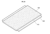
- FIG. 2b is a perspective view of the panel of FIG. 1 after a hydrophobic layer or surface treatment has been applied to the panel.
- FIG. 2c is a perspective view of a conductive ink being applied to the panel of FIG. 1 .
- FIG. 2d is a perspective of the panel of FIG. 1 coated with the conductive ink being heated.
- FIG. 1 is a flow chart illustrating a method of manufacturing an electromagnetic interference (EMI) shielding filter (i.e., an electromagnetic wave shield) for a plasma display panel in accordance with one embodiment of the present invention
- FIGS. 2a through 2d are perspective views illustrating a method of manufacturing an electromagnetic interference (EMI) shielding filter for a plasma display panel in accordance with one embodiment of the present invention.
- EMI electromagnetic interference
- the method of manufacturing the plasma display device in accordance with one embodiment of the present invention indudes a first panel preparation step (S1), a surface treatment step (S2), a conductive ink application step (S3) and a baking step (S4).
- the first panel preparation step (S1) is a step of preparing a first panel 110.
- the first panel 110 displays images and includes display electrodes to apply a voltage necessary for gas discharge of the plasma display device, and a dielectric layer formed on a first surface, the first surface facing a second panel 120 and being opposite to an image-displaying or second surface of the first panel 110.
- the panel 100 is shown in FIG. 1 as a combined form of the first panel 110 with the second panel 120, the first panel 110 alone may be prepared without being combined with the second panel 120.
- the second panel 120 includes address electrodes (not shown) adapted to apply a voltage necessary for gas discharge of the plasma display device and formed on a surface facing the first panel 110.
- the second panel 120 may further include an isolation wall, phosphors, a dielectric, and a protection film provided on the surface where the address electrodes were formed.
- the surface treatment step (S2) is a step of forming a hydrophobic layer 130 by applying a coating solution to the entirety of a second surface of the first panel 110, that is, the surface not facing to the second panel 120.
- the surface treatment step (S2) may employ fluoroalkylsilane (FAS) as a coating solution.
- FAS fluoroalkylsilane
- the fluoroalkylsilane is applied to the entire surface of the first panel 110 by a conventional method, e.g. printing or spin coating.
- the fluoroalkylsilane is a mixture of trichloro(3,3,3-trifluoropropyl)silane and trichloro(1H,1H,2H,2H-perfluorooctyl)silane.
- the ratio of volumes of the mixture of trichloro(3,3,3-trifluoropropyl)silane and trichloro(1H,1H,2H,2H-perfluorooctyl)silane is between about 100:1 to about 20:1, and in one embodiment may be about 60:1. If the ratio of the volumes is greater than 100:1, a hydrophobic effect of the FAS may be insufficient and if the ratio is less than 20:1, the hydrophobic effect of the FAS may be excessive. However, it will be appreciated that if a different type of conductive ink is used for the EMI shielding filter, as described in more detail below, the volume ratios of the mixture may be different.
- the concentration of FAS is between about 0.05M and about 0.3M in n-octane, and in one embodiment, the concentration may be about 0.1 M. If the concentration is less than about 0.05M, a hydrophobic effect of the FAS may be insufficient and if the concentration is greater than about 0.3M, excess FAS may be used.
- the hydrophobic layer 130 formed of FAS serves to control running and spreading of conductive ink on the surface of the first panel 110 to prevent excessive running and spreading which may occur upon application of the conductive ink in the subsequent conductive ink application step(S3).
- the hydrophobic layer 130 is formed of fluoroalkylsilane induding only trichloro(3,3,3-trifluoropropyl)silane without trichloro(1H,1H,2H,2H-perfluorooctyl)silane, spreadability of the conductive ink on the hydrophobic layer 130 is increased upon application of the conductive ink in the subsequent conductive ink application step (S3). As a result, it is difficult to form a conductive mesh pattern having a fine line-width of less than 100 ⁇ m on the hydrophobic layer 130.
- the FAS may be mixed with another compound such as 3-aminopropyl triethoxy silane and/or 3-mercaptopropyl triethoxy silane to be used as a surface treatment agent.
- the conductive ink application step (S3) is a step of forming a conductive mesh pattern (140 of FIG. 2d ) by applying the conductive ink to the hydrophobic layer 130.
- the conductive ink application step (S3) may employ a silver nano ink as a conductive ink.
- the silver nano-ink may be a dispersion of silver nano-particles having a particle diameter of about 5 nm to about 100 nm in n-tetadecane. If a particle diameter of the silver nano-particles is less than about 5 nm, this may result in non-uniform dispersion of the silver nano-particles. On the other hand, if a particle diameter of the silver nano-particles is larger than about 100 nm, this may result in plugging of flow paths of the silver nano-ink in a plurality of nozzles 11 of an ink-jet applicator 10.
- the conductive ink does not have to be a silver nano-ink, but rather may be other types of conductive ink including other materials such as copper.
- a content of the silver nano-particles may be in the range of about 50wt% to about 90wt% in the silver nano-ink, and the silver nano-ink may further include trace amounts of organic dispersant and inorganic frit in order to improve dispersibility and viscosity thereof. If a content of the silver nano-particles is less than about 50wt% of the silver nano-ink, this may lead to deterioration of electrical properties of the silver nano-ink.
- a content of the silver nano-particles is greater than about 90wt% of the silver nano-ink, a content of the organic dispersant and inorganic frit in the silver nano-ink is decreased to thereby result in less improvement of the dispersibility and viscosity of the silver nano-ink.
- the conductive ink application step (S3) includes application of the silver nano-ink to the hydrophobic layer 130 in an ink-jet manner using the ink-jet applicator 10, thus forming a conductive mesh pattern 140 where individual ink drops 140' are connected to one another.
- the conductive mesh pattern 140 has a line width with repeated thick and thin portions due to intrinsic nature of ink jet application.
- a thickness variation of a line formed by conductive ink drops can be controlled by varying the distance between each ink drop.
- an average ratio of thickest portion of the line to the thinnest portion of the line is between about 1.0:0.6 and about 1.0:0.9, and in one embodiment the ratio is 1.0:0.7. If the distance between each ink drop is too large, the sheet resistance may increase thereby degrading the shield performance. If the distance is too small, too much ink may be used to form the line.
- the conductive mesh pattern 140 is electrically connected to a ground of the plasma display device such that electromagnetic waves coming from the plasma display panel 100 are grounded to the ground of the plasma display device, thus shielding electromagnetic wave interference.
- FIG. 2c shows the state prior to complete formation of the conductive mesh patern 140 on the hydrophobic layer 130, with the size of the ink drops 140' of the conductive mesh pattern 140 being exaggerated for darity, whereas FIG. 2d shows complete formation of the conductive mesh pattern 140.
- the conductive mesh pattern 140 in the present application is formed on an outside surface of the first panel 110 of the panel 100. It is desirable in one embodiment to have the conductive mesh pattern 140 formed after fabrication of the panel 100 because as the first panel 110 and second panel 120 are moved through the production line, the conductive mesh pattern 140 can be damaged if formed prior to the fabrication of the panel 100. In other embodiments, the conductive mesh pattern 140 can be formed on the first panel 110 prior to the fabrication of the panel 100.
- the conductive ink application step S3 can apply the conductive ink to design and form a tetragonal conductive mesh pattern ( FIG. 2d ) having a pitch of about 200 ⁇ m to about 400 ⁇ m.
- pitch refers to the distance between two adjacent parallel lines that form the conductive mesh pattern. If a pitch of the conductive mesh pattern 140 is less than about 200 ⁇ m, a pitch of the conductive mesh pattern 140 becomes excessively dense to thereby lower light transmittance of the plasma display panel 100. On the other hand, if a pitch of the conductive mesh pattern 140 is higher than about 400 ⁇ m, an area of the conductive mesh pattern 140 occupied in the plasma display panel 100 is decreased to result in poor electromagnetic interference shielding efficiency of the plasma display panel 100.
- the conductive ink application step (S3) is performed in a manner that individual ink drops 140' being sprayed through multiple nozzles 11 of the ink-jet applicator 10 have a volume of about 3 pL to about 30 pL. If a volume of the individual ink drops 140' is less than about 3 pL, a line width of the conductive mesh pattern 140 is excessively thin to lower electrical conductivity in the plasma display panel 100. On the other hand, if a volume of the individual ink drops 140' is higher than about 30 pL, a line width of the conductive mesh pattern 140 is excessively thick to lower optical transmittance in the plasma display panel 100. In another embodiment, 12 pL is the upper limit for an ink drop volume. In still another embodiment, different sized ink drops may be used.
- Table 1 illustrates various droplet volumes and the corresponding line widths and mesh surface resistances produced for each volume, wherein the pitch of the conductive mesh pattern is about 300 ⁇ m.
- Table 1 Droplet volume (pL) Line width ( ⁇ m) Mesh surface resistance ( ⁇ /square) 3 32 0.4 4 34 0.33 8 40 0.20 20 60 0.11 30 70 0.05
- droplet volumes ranging from about 3 pL to about 30 pL produce line widths from between about 32 ⁇ m to about 70 ⁇ m and mesh surface resistances down to about 0.05 ⁇ /square.
- the baking step (S4) is a step of thermally baking the conductive mesh pattern 140 to be fixed on the hydrophobic layer 130.
- the baking step (S4) indudes fixation of the conductive mesh pattern 140 to the hydrophobic layer 130 by removing organic materials contained in the conductive mesh pattern 140 using heat of between about 250°C to about 400°C.
- hot air may be used to bake the conductive mesh pattern 140.
- a baking temperature of the conductive mesh pattern 140 is lower than about 250°C, the organic materials are not thoroughly removed from the conductive mesh pattern 140, thus resulting in deterioration of the electrical conductivity. On the other hand, if a baking temperature of the conductive mesh pattern 140 is higher than about 400°C, this may cause damage to the plasma display panel 100.
- the EMI shielding filter 150 including the hydrophobic layer 130 and the conductive mesh pattern 140 can have a line width of the conductive mesh pattern 140 of about 40 ⁇ m, light transmittance of about 77%, sheet resistance of about 0.2 ⁇ /square, and a pencil hardness of about 6H in response to a pencil hardness test. Where it is applied to a plasma display device, the EMI shielding filter 150 meets the FCC EMI Class B.
- the method of manufacturing an EMI shielding filter for a plasma display panel in accordance with one embodiment of the present invention can form an EMI shielding filter 150 including the hydrophobic layer 130 and the conductive mesh pattern 140 directly on the plasma display panel 100 by means of an ink-jet method using conductive ink.
- the method of manufacturing an EMI shielding filter for a plasma display panel in accordance with one embodiment of the present invention is capable of simplifying production processes and reducing production costs of a separate and additional base, as compared to fabrication of an EMI shielding filter through the formation of a conductive mesh pattern on a separate base by means of an etching process.
- the method of manufacturing an EMI shielding filter for a plasma display panel in accordance with one embodiment of the present invention is capable of saving production costs of a separate base and an expensive transparent conductive layer, as compared to fabrication of an EMI shielding filter through the formation of an expensive transparent conductive layer on a separate base.
- the method of manufacturing an EMI shielding filter for a plasma display panel in accordance with one embodiment of the present invention is capable of reducing the size of a plasma display device with the plasma display panel, due to no need of any additional base material in the formation of the EMI shielding filter.
Landscapes
- Engineering & Computer Science (AREA)
- Physics & Mathematics (AREA)
- Plasma & Fusion (AREA)
- Manufacturing & Machinery (AREA)
- Electromagnetism (AREA)
- Microelectronics & Electronic Packaging (AREA)
- Shielding Devices Or Components To Electric Or Magnetic Fields (AREA)
- Devices For Indicating Variable Information By Combining Individual Elements (AREA)
Claims (17)
- Verfahren zur Herstellung einer Plasmaanzeigetafel (100), das die folgenden Schritte umfasst :Herstellung einer ersten Tafel (110) der Plasmaanzeigetafel (100) mit einer ersten Fläche undeiner zweiten Fläche, wobei die zweite Fläche die Anzeigefläche der Plasmaanzeigetafel (100) ist; undBildung eines Schutzfilters gegen elektromagnetische Wellen (150) auf der zweiten Fläche der ersten Tafel (110), die die folgenden Schritte umfasst:- Bildung einer hydrophoben Schicht (130) durch Aufbringen einer Beschichtungslösung auf die zweite Fläche der ersten Tafel (110) (Schritt S2);- Bildung eines leitfähigen Gittermusters (140) auf einzelnen, miteinander verbundenen Tintentropfen (140'), die Leiterbahnen bilden, indem leitfähige Tinte durch Tintenstrahldruck direkt auf die hydrophobe Schicht (130) gedruckt wird (Schritt S3); und- Erwärmung der leitfähigen Tinte und der Beschichtungslösung, um das leitfähige Gittermuster (140) auf der hydrophoben Schicht zu fixieren (Schritt S4).
- Verfahren nach Anspruch 1, wobei die Beschichtungslösung auf die gesamte zweite Fläche der ersten Tafel (110) aufgetragen wird, und/oder wobei die Beschichtungslösung durch Drucken oder Rotationsbeschichtung (spin coating) aufgebracht wird.
- Verfahren nach Anspruch 1 oder 2, wobei die Beschichtungslösung Fluoralkylsilan (FAS) in einer Konzentration zwischen 0,05M und 0,3M aufweist.
- Verfahren nach Anspruch 3, wobei Fluoralkylsilan eine Mischung aus Trichlor(3,3,3-Trifluorpropyl)silan und Trichlor(1H, 1H, 2H, 2H-Perfluoroctyl)silan ist.
- Verfahren nach Anspruch 4, das weiterhin 3-Aminopropyltriethoxysilan und/oder 3-Mercaptopropyltriethoxysilan aufweist.
- Verfahren nach Anspruch 4 oder 5, wobei das Volumenverhältnis der Mischungen aus Trichlor(3,3,3-Trifluorpropyl)silan und Trichlor(1H, 1H, 2H, 2H-Perfluoroctyl)silan zwischen 100:1 und 20:1 beträgt.
- Verfahren nach Anspruch 1, wobei die einzelnen Tintentropfen (140') ein Volumen von 3 pL bis 30 pL besitzen.
- Verfahren nach einem der vorhergehenden Ansprüche, wobei die leitfähige Tinte eine Silbernanotinte ist und/oder die leitfähige Tinte Spurenmengen eines organischen Dispergens und inorganischer Fritte besitzt.
- Verfahren nach Anspruch 8, wobei die Silbernanotinte eine Dispersion von Silbernanopartikeln mit einem Partikeldurchmesser von 5 nm bis 100 nm in n-Tetradecan ist und/oder der Gehalt an Silbernanopartikeln in der leitfähigen Tinte in dem Bereich zwischen 50 Gewichtsprozent und 90 Gewichtsprozent liegt.
- Verfahren nach einem der vorhergehenden Ansprüche, wobei der Schritt der Erwärmung (S4) das Erwärmen des leitfähigen Gittermusters (140) und der hydrophoben Schicht (130) auf eine Temperatur umfasst, bei der organische Materialien aus dem leitfähigen Gittermuster (140) entfernt werden, und/oder wobei der Schritt der Erwärmung (S4) ein Erwärmen auf Temperaturen zwischen 250 °C und 400 °C umfasst.
- Verfahren nach einem der vorhergehenden Ansprüche, wobei das leitfähige Gittermuster (140):eine Linienbreite von 30 bis 70 µm besitzt; und/odereinen Oberflächenwiderstand des Gittermusters von 0,05 bis 0,4 Ω/Quadrat besitzt; und/oder ein tetragonales Muster einer Vielzahl der Leiterbahnen mit einem Abstand zwischen 200 µm und 400 µm bildet; und/oderaus einer Vielzahl der Leiterbahnen gebildet ist, die aus den einzelnen, miteinander verbundenen Tintentropfen gebildet werden, mit einer Linienbreite wiederholter breiter undschmaler Abschnitte mit einem durchschnittlichen Verhältnis des breitesten Abschnittes zu dem schmalsten Abschnitt jeder der Vielzahl der Leiterbahnen zwischen 1,0:0,6 und 1,0:0,9.
- Verfahren nach einem der vorhergehenden Ansprüche, wobei die hydrophobe Schicht (130) durch direktes Aufbringen einer Beschichtungslösung auf die erste Tafel (110) gebildet ist.
- Verfahren nach Anspruch nach einem der vorhergehenden Ansprüche, wobei das leitfähige Gittermuster (140) direkt an einer Außenfläche des Frontglases der Plasmaanzeigetafel (100) gebildet ist, und/oder wobei das leitfähige Gittermuster (140) als letzter Herstellungsschritt der Plasmaanzeigetafel (100) gebildet wird.
- Plasmaanzeigetafel (100) mit:einer ersten Tafel (110) mit einer ersten Fläche und einer zweiten Fläche, wobei die zweite Fläche die Anzeigefläche der Plasmaanzeigetafel (100) ist; undeinem Schutzfilter gegen elektromagnetische Wellen (150) an der zweiten Fläche der ersten Tafel (110),der Schutzfilter gegen elektromagnetische Wellen (150) besitzt eine hydrophobe Schicht (130), die sich direkt auf der zweiten Fläche befindet, und ein leitfähiges Gittermuster (140), das sich direkt auf der hydrophoben Schicht (130) befindet, dadurch gekennzeichnet, dass das leitfähige Gittermuster aus mit Tintenstrahldruck gedruckten, einzelnen Tintentropfen (140') gebildet ist, die miteinander verbunden sind, und Leiterbahnen des Gittermusters bilden.
- Plasmaanzeigetafel (100) nach Anspruch 14, wobei das leitfähige Gittermuster (140):eine Bahnbreite von 30 bis 70 µm besitzt; und/odereinen Oberflächenwiderstand des Gittermusters von 0,05 bis 0,4 Ω/Quadrat besitzt; und/oder ein tetragonales Muster einer Vielzahl von Leiterbahnen mit einem Abstand zwischen 200 µm und 400 µm bildet; und/oderaus einer Vielzahl von Leiterbahnen gebildet ist, die aus den einzelnen, miteinander verbundenen Tintentropfen gebildet werden, mit einer Linienbreite wiederholter breiter undschmaler Abschnitte mit einem durchschnittlichen Verhältnis des breitesten Abschnittes zu dem schmalsten Abschnitt jeder der Vielzahl von Leiterbahnen zwischen 1,0:0,6 und 1,0:0,9.
- Plasmaanzeigetafel (100) nach Anspruch 14 oder 15, wobei die hydrophobe Schicht Fluoralkylsilan aufweist.
- Plasmaanzeigetafel (100) nach einem der Ansprüche 14 bis 16, wobei das leitfähige Gittermuster Silbernanopartikel aufweist oder aus ihnen besteht.
Applications Claiming Priority (2)
| Application Number | Priority Date | Filing Date | Title |
|---|---|---|---|
| US14205708P | 2008-12-31 | 2008-12-31 | |
| US12/630,832 US8198810B2 (en) | 2008-12-31 | 2009-12-03 | Method of manufacturing electromagnetic interference (EMI) shielding filter for plasma display panel and EMI shielding filter for plasma display panel using the same |
Publications (2)
| Publication Number | Publication Date |
|---|---|
| EP2204837A1 EP2204837A1 (de) | 2010-07-07 |
| EP2204837B1 true EP2204837B1 (de) | 2011-05-18 |
Family
ID=41821938
Family Applications (1)
| Application Number | Title | Priority Date | Filing Date |
|---|---|---|---|
| EP20090179403 Active EP2204837B1 (de) | 2008-12-31 | 2009-12-16 | Verfahren zur Herstellung eines Schutzfilters gegen elektromagnetische Interferenzen (EMI) für Plasmaanzeigetafel und EMI-Schutzfilter für Plasmaanzeigetafel damit |
Country Status (5)
| Country | Link |
|---|---|
| US (1) | US8198810B2 (de) |
| EP (1) | EP2204837B1 (de) |
| KR (1) | KR101106430B1 (de) |
| CN (1) | CN101820739B (de) |
| AT (1) | ATE510296T1 (de) |
Families Citing this family (7)
| Publication number | Priority date | Publication date | Assignee | Title |
|---|---|---|---|---|
| US9302452B2 (en) * | 2012-03-02 | 2016-04-05 | Ppg Industries Ohio, Inc. | Transparent laminates comprising inkjet printed conductive lines and methods of forming the same |
| KR101394189B1 (ko) * | 2013-09-11 | 2014-05-14 | 한국에너지기술연구원 | 잉크젯 프린팅 기법을 이용한 풍력 발전기용 회전 날개 및 제작 방법 |
| CN109435513B (zh) * | 2018-10-22 | 2020-09-18 | 北京印刷学院 | 基于涂布方式制备纸基电极的方法 |
| US11745702B2 (en) | 2018-12-11 | 2023-09-05 | Ppg Industries Ohio, Inc. | Coating including electrically conductive lines directly on electrically conductive layer |
| CN111128702A (zh) * | 2019-12-10 | 2020-05-08 | Tcl华星光电技术有限公司 | 一种金属电极的制备方法 |
| CN111554633B (zh) * | 2020-05-20 | 2022-09-20 | 业成科技(成都)有限公司 | 导电层图案化的方法及导电结构 |
| CN113488497A (zh) * | 2021-06-24 | 2021-10-08 | 深圳市华星光电半导体显示技术有限公司 | 一种显示面板及其制备方法、显示装置 |
Family Cites Families (21)
| Publication number | Priority date | Publication date | Assignee | Title |
|---|---|---|---|---|
| SE9703410D0 (sv) * | 1997-09-22 | 1997-09-22 | Ericsson Telefon Ab L M | Sätt att överföra en bild på oregelbundna ytor |
| US6255778B1 (en) * | 1997-10-13 | 2001-07-03 | Bridgestone Corporation | Plasma display panel having electromagnetic wave shielding material attached to front surface of display |
| JP4013021B2 (ja) | 1999-12-17 | 2007-11-28 | 松下電工株式会社 | 透視性電磁波シールド材及びその製造方法 |
| JP2003297567A (ja) | 2002-04-04 | 2003-10-17 | Sekisui Chem Co Ltd | パターン形成用基板及び有機el素子 |
| KR100999291B1 (ko) | 2002-07-22 | 2010-12-07 | 삼성코닝정밀소재 주식회사 | 금속 메쉬 필름 상의 투명층 코팅방법 |
| WO2004039138A1 (ja) * | 2002-10-28 | 2004-05-06 | Bridgestone Corporation | 電磁波シールド性光透過窓材及びその製造方法 |
| JP4332360B2 (ja) * | 2003-02-28 | 2009-09-16 | 大日本印刷株式会社 | 濡れ性パターン形成用塗工液およびパターン形成体の製造方法 |
| KR100518857B1 (ko) | 2003-11-07 | 2005-09-30 | 엘지전자 주식회사 | 잉크젯 방식의 전극 제조방법 |
| CN1879253A (zh) * | 2003-11-12 | 2006-12-13 | 株式会社秀峰 | 天线图案以及具有其的电磁波能量处理装置 |
| WO2005072040A1 (ja) * | 2004-01-21 | 2005-08-04 | Dai Nippon Printing Co., Ltd. | 電磁波シールドフィルム、及びその製造方法 |
| KR100757519B1 (ko) | 2005-01-27 | 2007-09-11 | 한국화학연구원 | 잉크젯 방식에 의한 플라즈마 디스플레이 패널용 전극의제조방법 |
| KR100735411B1 (ko) | 2005-12-07 | 2007-07-04 | 삼성전기주식회사 | 배선기판의 제조방법 및 배선기판 |
| JP4438800B2 (ja) * | 2006-02-13 | 2010-03-24 | セイコーエプソン株式会社 | 液滴吐出装置 |
| JP4967437B2 (ja) | 2006-04-27 | 2012-07-04 | 旭硝子株式会社 | 透明導電膜の製造方法および透明導電膜 |
| JP2008000733A (ja) | 2006-06-26 | 2008-01-10 | Asahi Glass Co Ltd | パターン形成基材の製造方法 |
| EP2052043B1 (de) * | 2006-08-07 | 2016-10-12 | Inktec Co., Ltd. | Verfahren zur herstellung von silbernanopartikeln sowie silbertintenzusammensetzungen damit |
| JP4872600B2 (ja) * | 2006-10-27 | 2012-02-08 | 富士ゼロックス株式会社 | 電子写真感光体、電子写真感光体の製造方法、プロセスカートリッジ、および画像形成装置 |
| KR100905970B1 (ko) | 2007-03-09 | 2009-07-06 | 주식회사 동진쎄미켐 | 흑색 도전성 페이스트 조성물, 이를 포함하는 전자파차폐용 필터 및 표시 장치 |
| WO2008111757A1 (en) | 2007-03-09 | 2008-09-18 | Dongjin Semichem Co., Ltd | Black paste composition having conductivity property, filter for shielding electromagnetic interference and display device comprising the same} |
| JP2008305829A (ja) * | 2007-06-05 | 2008-12-18 | Mitsubishi Gas Chem Co Inc | 光干渉縞防止光透過型電磁波シールド材料 |
| US20090053507A1 (en) * | 2007-08-17 | 2009-02-26 | Ndsu Research Foundation | Convergent-divergent-convergent nozzle focusing of aerosol particles for micron-scale direct writing |
-
2009
- 2009-12-03 US US12/630,832 patent/US8198810B2/en not_active Expired - Fee Related
- 2009-12-09 KR KR1020090122089A patent/KR101106430B1/ko not_active Expired - Fee Related
- 2009-12-16 EP EP20090179403 patent/EP2204837B1/de active Active
- 2009-12-16 AT AT09179403T patent/ATE510296T1/de not_active IP Right Cessation
- 2009-12-24 CN CN2009102599948A patent/CN101820739B/zh not_active Expired - Fee Related
Also Published As
| Publication number | Publication date |
|---|---|
| KR101106430B1 (ko) | 2012-01-18 |
| EP2204837A1 (de) | 2010-07-07 |
| ATE510296T1 (de) | 2011-06-15 |
| KR20100080365A (ko) | 2010-07-08 |
| CN101820739A (zh) | 2010-09-01 |
| US20100164354A1 (en) | 2010-07-01 |
| CN101820739B (zh) | 2013-02-20 |
| US8198810B2 (en) | 2012-06-12 |
Similar Documents
| Publication | Publication Date | Title |
|---|---|---|
| EP2204837B1 (de) | Verfahren zur Herstellung eines Schutzfilters gegen elektromagnetische Interferenzen (EMI) für Plasmaanzeigetafel und EMI-Schutzfilter für Plasmaanzeigetafel damit | |
| US20130078457A1 (en) | Method of forming metal oxide film, metal oxide film and optical electronic device | |
| KR20020080500A (ko) | 플라즈마 디스플레이 패널 및 그 제조방법 | |
| TW200425213A (en) | Device, method of manufacturing the same, electro-optic device, and electronic equipment | |
| US7914713B2 (en) | Ink-based electromagnetic-wave shielding film for display device | |
| KR102088100B1 (ko) | 광소결 나노잉크, 광소결 방법 그리고 전도성 나노 구조체 | |
| US20090026952A1 (en) | Phosphor paste and plasma display panel using the same | |
| EP1931190A1 (de) | Flachdisplay-glied und verfahren zu seiner herstellung und flachdisplay und verfahren zu seiner herstellung | |
| CN1285094C (zh) | 等离子显示板及其制造方法 | |
| JP5082391B2 (ja) | 透明導電膜の作製方法、透明導電膜及びプラズマディスプレイ用電磁波シールド | |
| EP1967871A2 (de) | Filter und Anzeigevorrichtung damit | |
| JP5602510B2 (ja) | 透明導電フィルム、それを用いた電磁波シールド材及びタッチセンサー、並びにそれらの製造方法 | |
| KR101729758B1 (ko) | 저온 소결용 구리 나노 잉크를 이용한 적층형 디지타이저 및 이의 제조방법 | |
| JP4589980B2 (ja) | プラズマディスプレイパネルの製造方法 | |
| JP4360524B2 (ja) | プラズマディスプレイパネル用基板の製造方法及び該基板を用いたプラズマディスプレイパネル | |
| JP4923293B2 (ja) | 微細ラインの形成方法 | |
| CN1346504A (zh) | 等离子体显示板的制造方法 | |
| CN1753136A (zh) | 等离子体显示屏、其制造方法及阻挡壁 | |
| JP2004071248A (ja) | プラズマディスプレイ及びその製造方法 | |
| EP1742244A2 (de) | Herstellungsmethode einer Plasmaanzeigetafel | |
| KR101002460B1 (ko) | 첨가제가 포함된 입자 함유 잉크 | |
| KR20100092586A (ko) | 플라즈마 디스플레이 패널 및 그 제조 방법 | |
| EP1798747A2 (de) | Methode zur Herstellung einer dielektrischen Schicht einer Plasmaanzeigetafel | |
| KR20080009912A (ko) | 디스플레이 장치의 전면필터 및 그 제조방법 | |
| KR20100092587A (ko) | 플라즈마 디스플레이 패널 및 그 제조 방법 |
Legal Events
| Date | Code | Title | Description |
|---|---|---|---|
| PUAI | Public reference made under article 153(3) epc to a published international application that has entered the european phase |
Free format text: ORIGINAL CODE: 0009012 |
|
| 17P | Request for examination filed |
Effective date: 20091216 |
|
| AK | Designated contracting states |
Kind code of ref document: A1 Designated state(s): AT BE BG CH CY CZ DE DK EE ES FI FR GB GR HR HU IE IS IT LI LT LU LV MC MK MT NL NO PL PT RO SE SI SK SM TR |
|
| AX | Request for extension of the european patent |
Extension state: AL BA RS |
|
| GRAP | Despatch of communication of intention to grant a patent |
Free format text: ORIGINAL CODE: EPIDOSNIGR1 |
|
| RIC1 | Information provided on ipc code assigned before grant |
Ipc: H01J 17/49 20060101AFI20101021BHEP |
|
| RIN1 | Information on inventor provided before grant (corrected) |
Inventor name: SEO, SANGCHUL Inventor name: PAEK, SEUNGHYUCK Inventor name: PYO, YOUNGHAK Inventor name: JU, RIA Inventor name: YOON, HEEYOUL Inventor name: KIM, MINHYUNG Inventor name: JIN, SANGYOUNG Inventor name: LIM, JAESEOK |
|
| GRAS | Grant fee paid |
Free format text: ORIGINAL CODE: EPIDOSNIGR3 |
|
| GRAA | (expected) grant |
Free format text: ORIGINAL CODE: 0009210 |
|
| REG | Reference to a national code |
Ref country code: GB Ref legal event code: FG4D |
|
| REG | Reference to a national code |
Ref country code: CH Ref legal event code: EP |
|
| REG | Reference to a national code |
Ref country code: IE Ref legal event code: FG4D |
|
| REG | Reference to a national code |
Ref country code: DE Ref legal event code: R096 Ref document number: 602009001299 Country of ref document: DE Effective date: 20110630 |
|
| REG | Reference to a national code |
Ref country code: NL Ref legal event code: VDEP Effective date: 20110518 |
|
| PG25 | Lapsed in a contracting state [announced via postgrant information from national office to epo] |
Ref country code: HR Free format text: LAPSE BECAUSE OF FAILURE TO SUBMIT A TRANSLATION OF THE DESCRIPTION OR TO PAY THE FEE WITHIN THE PRESCRIBED TIME-LIMIT Effective date: 20110518 Ref country code: NO Free format text: LAPSE BECAUSE OF FAILURE TO SUBMIT A TRANSLATION OF THE DESCRIPTION OR TO PAY THE FEE WITHIN THE PRESCRIBED TIME-LIMIT Effective date: 20110818 Ref country code: PT Free format text: LAPSE BECAUSE OF FAILURE TO SUBMIT A TRANSLATION OF THE DESCRIPTION OR TO PAY THE FEE WITHIN THE PRESCRIBED TIME-LIMIT Effective date: 20110919 Ref country code: LT Free format text: LAPSE BECAUSE OF FAILURE TO SUBMIT A TRANSLATION OF THE DESCRIPTION OR TO PAY THE FEE WITHIN THE PRESCRIBED TIME-LIMIT Effective date: 20110518 Ref country code: SE Free format text: LAPSE BECAUSE OF FAILURE TO SUBMIT A TRANSLATION OF THE DESCRIPTION OR TO PAY THE FEE WITHIN THE PRESCRIBED TIME-LIMIT Effective date: 20110518 |
|
| PG25 | Lapsed in a contracting state [announced via postgrant information from national office to epo] |
Ref country code: BE Free format text: LAPSE BECAUSE OF FAILURE TO SUBMIT A TRANSLATION OF THE DESCRIPTION OR TO PAY THE FEE WITHIN THE PRESCRIBED TIME-LIMIT Effective date: 20110518 Ref country code: AT Free format text: LAPSE BECAUSE OF FAILURE TO SUBMIT A TRANSLATION OF THE DESCRIPTION OR TO PAY THE FEE WITHIN THE PRESCRIBED TIME-LIMIT Effective date: 20110518 Ref country code: GR Free format text: LAPSE BECAUSE OF FAILURE TO SUBMIT A TRANSLATION OF THE DESCRIPTION OR TO PAY THE FEE WITHIN THE PRESCRIBED TIME-LIMIT Effective date: 20110819 Ref country code: CY Free format text: LAPSE BECAUSE OF FAILURE TO SUBMIT A TRANSLATION OF THE DESCRIPTION OR TO PAY THE FEE WITHIN THE PRESCRIBED TIME-LIMIT Effective date: 20110518 Ref country code: SI Free format text: LAPSE BECAUSE OF FAILURE TO SUBMIT A TRANSLATION OF THE DESCRIPTION OR TO PAY THE FEE WITHIN THE PRESCRIBED TIME-LIMIT Effective date: 20110518 Ref country code: FI Free format text: LAPSE BECAUSE OF FAILURE TO SUBMIT A TRANSLATION OF THE DESCRIPTION OR TO PAY THE FEE WITHIN THE PRESCRIBED TIME-LIMIT Effective date: 20110518 Ref country code: ES Free format text: LAPSE BECAUSE OF FAILURE TO SUBMIT A TRANSLATION OF THE DESCRIPTION OR TO PAY THE FEE WITHIN THE PRESCRIBED TIME-LIMIT Effective date: 20110829 Ref country code: IS Free format text: LAPSE BECAUSE OF FAILURE TO SUBMIT A TRANSLATION OF THE DESCRIPTION OR TO PAY THE FEE WITHIN THE PRESCRIBED TIME-LIMIT Effective date: 20110918 Ref country code: LV Free format text: LAPSE BECAUSE OF FAILURE TO SUBMIT A TRANSLATION OF THE DESCRIPTION OR TO PAY THE FEE WITHIN THE PRESCRIBED TIME-LIMIT Effective date: 20110518 |
|
| PG25 | Lapsed in a contracting state [announced via postgrant information from national office to epo] |
Ref country code: NL Free format text: LAPSE BECAUSE OF FAILURE TO SUBMIT A TRANSLATION OF THE DESCRIPTION OR TO PAY THE FEE WITHIN THE PRESCRIBED TIME-LIMIT Effective date: 20110518 |
|
| PG25 | Lapsed in a contracting state [announced via postgrant information from national office to epo] |
Ref country code: EE Free format text: LAPSE BECAUSE OF FAILURE TO SUBMIT A TRANSLATION OF THE DESCRIPTION OR TO PAY THE FEE WITHIN THE PRESCRIBED TIME-LIMIT Effective date: 20110518 Ref country code: CZ Free format text: LAPSE BECAUSE OF FAILURE TO SUBMIT A TRANSLATION OF THE DESCRIPTION OR TO PAY THE FEE WITHIN THE PRESCRIBED TIME-LIMIT Effective date: 20110518 |
|
| PG25 | Lapsed in a contracting state [announced via postgrant information from national office to epo] |
Ref country code: PL Free format text: LAPSE BECAUSE OF FAILURE TO SUBMIT A TRANSLATION OF THE DESCRIPTION OR TO PAY THE FEE WITHIN THE PRESCRIBED TIME-LIMIT Effective date: 20110518 Ref country code: SK Free format text: LAPSE BECAUSE OF FAILURE TO SUBMIT A TRANSLATION OF THE DESCRIPTION OR TO PAY THE FEE WITHIN THE PRESCRIBED TIME-LIMIT Effective date: 20110518 |
|
| PLBE | No opposition filed within time limit |
Free format text: ORIGINAL CODE: 0009261 |
|
| STAA | Information on the status of an ep patent application or granted ep patent |
Free format text: STATUS: NO OPPOSITION FILED WITHIN TIME LIMIT |
|
| 26N | No opposition filed |
Effective date: 20120221 |
|
| PG25 | Lapsed in a contracting state [announced via postgrant information from national office to epo] |
Ref country code: IT Free format text: LAPSE BECAUSE OF FAILURE TO SUBMIT A TRANSLATION OF THE DESCRIPTION OR TO PAY THE FEE WITHIN THE PRESCRIBED TIME-LIMIT Effective date: 20110518 |
|
| REG | Reference to a national code |
Ref country code: DE Ref legal event code: R097 Ref document number: 602009001299 Country of ref document: DE Effective date: 20120221 |
|
| PG25 | Lapsed in a contracting state [announced via postgrant information from national office to epo] |
Ref country code: MC Free format text: LAPSE BECAUSE OF NON-PAYMENT OF DUE FEES Effective date: 20111231 |
|
| REG | Reference to a national code |
Ref country code: IE Ref legal event code: MM4A |
|
| PG25 | Lapsed in a contracting state [announced via postgrant information from national office to epo] |
Ref country code: IE Free format text: LAPSE BECAUSE OF NON-PAYMENT OF DUE FEES Effective date: 20111216 |
|
| PG25 | Lapsed in a contracting state [announced via postgrant information from national office to epo] |
Ref country code: MT Free format text: LAPSE BECAUSE OF FAILURE TO SUBMIT A TRANSLATION OF THE DESCRIPTION OR TO PAY THE FEE WITHIN THE PRESCRIBED TIME-LIMIT Effective date: 20110518 Ref country code: MK Free format text: LAPSE BECAUSE OF FAILURE TO SUBMIT A TRANSLATION OF THE DESCRIPTION OR TO PAY THE FEE WITHIN THE PRESCRIBED TIME-LIMIT Effective date: 20110518 |
|
| PG25 | Lapsed in a contracting state [announced via postgrant information from national office to epo] |
Ref country code: SM Free format text: LAPSE BECAUSE OF FAILURE TO SUBMIT A TRANSLATION OF THE DESCRIPTION OR TO PAY THE FEE WITHIN THE PRESCRIBED TIME-LIMIT Effective date: 20110518 |
|
| PG25 | Lapsed in a contracting state [announced via postgrant information from national office to epo] |
Ref country code: LU Free format text: LAPSE BECAUSE OF NON-PAYMENT OF DUE FEES Effective date: 20111216 |
|
| PG25 | Lapsed in a contracting state [announced via postgrant information from national office to epo] |
Ref country code: BG Free format text: LAPSE BECAUSE OF FAILURE TO SUBMIT A TRANSLATION OF THE DESCRIPTION OR TO PAY THE FEE WITHIN THE PRESCRIBED TIME-LIMIT Effective date: 20110818 |
|
| PG25 | Lapsed in a contracting state [announced via postgrant information from national office to epo] |
Ref country code: TR Free format text: LAPSE BECAUSE OF FAILURE TO SUBMIT A TRANSLATION OF THE DESCRIPTION OR TO PAY THE FEE WITHIN THE PRESCRIBED TIME-LIMIT Effective date: 20110518 |
|
| PG25 | Lapsed in a contracting state [announced via postgrant information from national office to epo] |
Ref country code: HU Free format text: LAPSE BECAUSE OF FAILURE TO SUBMIT A TRANSLATION OF THE DESCRIPTION OR TO PAY THE FEE WITHIN THE PRESCRIBED TIME-LIMIT Effective date: 20110518 |
|
| PGFP | Annual fee paid to national office [announced via postgrant information from national office to epo] |
Ref country code: DE Payment date: 20131113 Year of fee payment: 5 Ref country code: GB Payment date: 20131112 Year of fee payment: 5 Ref country code: FR Payment date: 20131115 Year of fee payment: 5 |
|
| REG | Reference to a national code |
Ref country code: CH Ref legal event code: PL |
|
| PG25 | Lapsed in a contracting state [announced via postgrant information from national office to epo] |
Ref country code: LI Free format text: LAPSE BECAUSE OF NON-PAYMENT OF DUE FEES Effective date: 20131231 Ref country code: CH Free format text: LAPSE BECAUSE OF NON-PAYMENT OF DUE FEES Effective date: 20131231 |
|
| REG | Reference to a national code |
Ref country code: DE Ref legal event code: R119 Ref document number: 602009001299 Country of ref document: DE |
|
| GBPC | Gb: european patent ceased through non-payment of renewal fee |
Effective date: 20141216 |
|
| REG | Reference to a national code |
Ref country code: FR Ref legal event code: ST Effective date: 20150831 |
|
| PG25 | Lapsed in a contracting state [announced via postgrant information from national office to epo] |
Ref country code: GB Free format text: LAPSE BECAUSE OF NON-PAYMENT OF DUE FEES Effective date: 20141216 Ref country code: DE Free format text: LAPSE BECAUSE OF NON-PAYMENT OF DUE FEES Effective date: 20150701 |
|
| PG25 | Lapsed in a contracting state [announced via postgrant information from national office to epo] |
Ref country code: FR Free format text: LAPSE BECAUSE OF NON-PAYMENT OF DUE FEES Effective date: 20141231 |