EP2204881A1 - Breitbandige Antenne mit einem U-förmigen Antennenleiter - Google Patents
Breitbandige Antenne mit einem U-förmigen Antennenleiter Download PDFInfo
- Publication number
- EP2204881A1 EP2204881A1 EP10156367A EP10156367A EP2204881A1 EP 2204881 A1 EP2204881 A1 EP 2204881A1 EP 10156367 A EP10156367 A EP 10156367A EP 10156367 A EP10156367 A EP 10156367A EP 2204881 A1 EP2204881 A1 EP 2204881A1
- Authority
- EP
- European Patent Office
- Prior art keywords
- conductor
- antenna
- antenna device
- end side
- base body
- Prior art date
- Legal status (The legal status is an assumption and is not a legal conclusion. Google has not performed a legal analysis and makes no representation as to the accuracy of the status listed.)
- Withdrawn
Links
- 239000004020 conductor Substances 0.000 title claims abstract description 715
- 239000011810 insulating material Substances 0.000 claims abstract description 14
- 229910052751 metal Inorganic materials 0.000 claims description 95
- 239000002184 metal Substances 0.000 claims description 95
- 238000004891 communication Methods 0.000 claims description 27
- 239000011888 foil Substances 0.000 claims description 21
- 230000005684 electric field Effects 0.000 abstract description 3
- 238000010586 diagram Methods 0.000 description 60
- 230000005855 radiation Effects 0.000 description 41
- 230000008878 coupling Effects 0.000 description 18
- 238000010168 coupling process Methods 0.000 description 18
- 238000005859 coupling reaction Methods 0.000 description 18
- 239000003989 dielectric material Substances 0.000 description 17
- 238000000034 method Methods 0.000 description 14
- 229910000859 α-Fe Inorganic materials 0.000 description 14
- 239000000696 magnetic material Substances 0.000 description 12
- 239000004033 plastic Substances 0.000 description 12
- 239000000463 material Substances 0.000 description 11
- RYGMFSIKBFXOCR-UHFFFAOYSA-N Copper Chemical compound [Cu] RYGMFSIKBFXOCR-UHFFFAOYSA-N 0.000 description 10
- 239000000919 ceramic Substances 0.000 description 10
- 230000000694 effects Effects 0.000 description 10
- 238000007747 plating Methods 0.000 description 10
- 229910000906 Bronze Inorganic materials 0.000 description 8
- 229910019142 PO4 Inorganic materials 0.000 description 8
- VYPSYNLAJGMNEJ-UHFFFAOYSA-N Silicium dioxide Chemical compound O=[Si]=O VYPSYNLAJGMNEJ-UHFFFAOYSA-N 0.000 description 8
- 239000010974 bronze Substances 0.000 description 8
- 239000011889 copper foil Substances 0.000 description 8
- KUNSUQLRTQLHQQ-UHFFFAOYSA-N copper tin Chemical compound [Cu].[Sn] KUNSUQLRTQLHQQ-UHFFFAOYSA-N 0.000 description 8
- NBIIXXVUZAFLBC-UHFFFAOYSA-K phosphate Chemical compound [O-]P([O-])([O-])=O NBIIXXVUZAFLBC-UHFFFAOYSA-K 0.000 description 8
- 239000010452 phosphate Substances 0.000 description 8
- 238000007650 screen-printing Methods 0.000 description 8
- 239000000853 adhesive Substances 0.000 description 7
- 230000001070 adhesive effect Effects 0.000 description 7
- 230000003247 decreasing effect Effects 0.000 description 7
- PCHJSUWPFVWCPO-UHFFFAOYSA-N gold Chemical compound [Au] PCHJSUWPFVWCPO-UHFFFAOYSA-N 0.000 description 7
- 229910052737 gold Inorganic materials 0.000 description 7
- 239000010931 gold Substances 0.000 description 7
- 239000000126 substance Substances 0.000 description 7
- 238000004519 manufacturing process Methods 0.000 description 6
- PXHVJJICTQNCMI-UHFFFAOYSA-N nickel Substances [Ni] PXHVJJICTQNCMI-UHFFFAOYSA-N 0.000 description 6
- 238000007639 printing Methods 0.000 description 6
- 230000009467 reduction Effects 0.000 description 6
- 238000005476 soldering Methods 0.000 description 6
- 230000009471 action Effects 0.000 description 5
- 238000003754 machining Methods 0.000 description 5
- 238000005259 measurement Methods 0.000 description 5
- FYYHWMGAXLPEAU-UHFFFAOYSA-N Magnesium Chemical compound [Mg] FYYHWMGAXLPEAU-UHFFFAOYSA-N 0.000 description 4
- PNEYBMLMFCGWSK-UHFFFAOYSA-N aluminium oxide Inorganic materials [O-2].[O-2].[O-2].[Al+3].[Al+3] PNEYBMLMFCGWSK-UHFFFAOYSA-N 0.000 description 4
- 238000000151 deposition Methods 0.000 description 4
- 229910052749 magnesium Inorganic materials 0.000 description 4
- 239000011777 magnesium Substances 0.000 description 4
- 238000004904 shortening Methods 0.000 description 4
- 239000000377 silicon dioxide Substances 0.000 description 4
- BQCADISMDOOEFD-UHFFFAOYSA-N Silver Chemical compound [Ag] BQCADISMDOOEFD-UHFFFAOYSA-N 0.000 description 3
- 230000000052 comparative effect Effects 0.000 description 3
- 239000003822 epoxy resin Substances 0.000 description 3
- 239000011521 glass Substances 0.000 description 3
- 230000006872 improvement Effects 0.000 description 3
- 229920000647 polyepoxide Polymers 0.000 description 3
- 230000008569 process Effects 0.000 description 3
- 230000035945 sensitivity Effects 0.000 description 3
- 229910052709 silver Inorganic materials 0.000 description 3
- 239000004332 silver Substances 0.000 description 3
- 230000015556 catabolic process Effects 0.000 description 2
- 239000011248 coating agent Substances 0.000 description 2
- 238000000576 coating method Methods 0.000 description 2
- 239000002131 composite material Substances 0.000 description 2
- 229910052802 copper Inorganic materials 0.000 description 2
- 239000010949 copper Substances 0.000 description 2
- 238000006731 degradation reaction Methods 0.000 description 2
- 238000013461 design Methods 0.000 description 2
- 229910052759 nickel Inorganic materials 0.000 description 2
- 229920005989 resin Polymers 0.000 description 2
- 239000011347 resin Substances 0.000 description 2
- 230000035939 shock Effects 0.000 description 2
- 230000008901 benefit Effects 0.000 description 1
- 230000005540 biological transmission Effects 0.000 description 1
- 230000015572 biosynthetic process Effects 0.000 description 1
- 230000008859 change Effects 0.000 description 1
- 230000008021 deposition Effects 0.000 description 1
- 238000011161 development Methods 0.000 description 1
- 238000005516 engineering process Methods 0.000 description 1
- 230000006870 function Effects 0.000 description 1
- 238000009413 insulation Methods 0.000 description 1
- 230000003993 interaction Effects 0.000 description 1
- 230000035699 permeability Effects 0.000 description 1
- 238000011160 research Methods 0.000 description 1
- 238000000926 separation method Methods 0.000 description 1
- 238000002834 transmittance Methods 0.000 description 1
Images
















Classifications
-
- H—ELECTRICITY
- H01—ELECTRIC ELEMENTS
- H01Q—ANTENNAS, i.e. RADIO AERIALS
- H01Q1/00—Details of, or arrangements associated with, antennas
- H01Q1/12—Supports; Mounting means
- H01Q1/22—Supports; Mounting means by structural association with other equipment or articles
- H01Q1/24—Supports; Mounting means by structural association with other equipment or articles with receiving set
-
- H—ELECTRICITY
- H01—ELECTRIC ELEMENTS
- H01Q—ANTENNAS, i.e. RADIO AERIALS
- H01Q1/00—Details of, or arrangements associated with, antennas
- H01Q1/12—Supports; Mounting means
- H01Q1/22—Supports; Mounting means by structural association with other equipment or articles
- H01Q1/24—Supports; Mounting means by structural association with other equipment or articles with receiving set
- H01Q1/241—Supports; Mounting means by structural association with other equipment or articles with receiving set used in mobile communications, e.g. GSM
- H01Q1/242—Supports; Mounting means by structural association with other equipment or articles with receiving set used in mobile communications, e.g. GSM specially adapted for hand-held use
- H01Q1/243—Supports; Mounting means by structural association with other equipment or articles with receiving set used in mobile communications, e.g. GSM specially adapted for hand-held use with built-in antennas
-
- H—ELECTRICITY
- H01—ELECTRIC ELEMENTS
- H01Q—ANTENNAS, i.e. RADIO AERIALS
- H01Q1/00—Details of, or arrangements associated with, antennas
- H01Q1/36—Structural form of radiating elements, e.g. cone, spiral, umbrella; Particular materials used therewith
-
- H—ELECTRICITY
- H01—ELECTRIC ELEMENTS
- H01Q—ANTENNAS, i.e. RADIO AERIALS
- H01Q1/00—Details of, or arrangements associated with, antennas
- H01Q1/36—Structural form of radiating elements, e.g. cone, spiral, umbrella; Particular materials used therewith
- H01Q1/38—Structural form of radiating elements, e.g. cone, spiral, umbrella; Particular materials used therewith formed by a conductive layer on an insulating support
-
- H—ELECTRICITY
- H01—ELECTRIC ELEMENTS
- H01Q—ANTENNAS, i.e. RADIO AERIALS
- H01Q5/00—Arrangements for simultaneous operation of antennas on two or more different wavebands, e.g. dual-band or multi-band arrangements
- H01Q5/30—Arrangements for providing operation on different wavebands
- H01Q5/307—Individual or coupled radiating elements, each element being fed in an unspecified way
- H01Q5/342—Individual or coupled radiating elements, each element being fed in an unspecified way for different propagation modes
- H01Q5/357—Individual or coupled radiating elements, each element being fed in an unspecified way for different propagation modes using a single feed point
- H01Q5/364—Creating multiple current paths
- H01Q5/371—Branching current paths
-
- H—ELECTRICITY
- H01—ELECTRIC ELEMENTS
- H01Q—ANTENNAS, i.e. RADIO AERIALS
- H01Q9/00—Electrically-short antennas having dimensions not more than twice the operating wavelength and consisting of conductive active radiating elements
- H01Q9/04—Resonant antennas
- H01Q9/30—Resonant antennas with feed to end of elongated active element, e.g. unipole
- H01Q9/42—Resonant antennas with feed to end of elongated active element, e.g. unipole with folded element, the folded parts being spaced apart a small fraction of the operating wavelength
Definitions
- Patent Reference 1 Japanese Patent Application Laid-open No. 2004-363789
- Patent Reference 2 Japanese Patent Application Laid-open No. 2004-7803
- Patent Reference 3 International Publication No.
- the antenna device disclosed in the Patent Reference 4 has another problem that an antenna needs to be installed for every band and space for the antenna device is greatly occupied by antenna circuits and its antenna gain is reduced due to fluctuations of directivity of the antenna and degradation in VSWR (Voltage Standing Wave Ratio) caused by interactions among the installed antennas for each band.
- the antenna device disclosed in the Patent Reference 5 has a problem that the antenna used is a single loop antenna in which its line length or electrical length consists of one wavelength and, therefore, space for the antenna is greatly occupied in the antenna device.
- the base body made of a dielectric material or magnetic material both being an insulating material is coupled to a place where an electric field strength of the conductor antenna increases and, as a result, an electromagnetic distance between the one end and the other end of the conductor antenna becomes short to a degree to which electrostatic coupling occurs, which allows a resonant point to be easily obtained and, therefore, the antenna can be miniaturized by a wavelength shortening effect of the dielectric or magnetic material being the insulating material. Therefore, the antenna device is allowed to operate in wide bands (in a multi-band) and to achieve excellent antenna gain and maintain non-directivity of vertically polarized waves and save space.
- an antenna device which includes an approximately U-shaped conductor antenna, on one end side of which a power feeding portion is provided and, on other end side of which an end portion is provided as an open end terminal and a base body made of an insulating material, wherein one end of the conductor antenna and other end of the conductor antenna are placed so as to come near to each other with the base body interposed between the one end of the conductor antenna and the other end of the conductor antenna and wherein the base body is coupled between the one end of the conductor antenna and other end of the conductor antenna.
- the conductor antenna is made of a metal conductive plate or a metal conductive line or the conductor antenna is constructed of a conductor pattern made of metal conductive foil placed on the base body or of a metal conductive film.
- an antenna device made up of an approximately U-shaped conductor antenna, on one end side of which a power feeding portion is provided and on the other end side of which an end portion is provided as an open end terminal and a base body made of an insulating material, wherein one end of the conductor antenna and other end of the conductor antenna are placed so as to come near to each other with the base body interposed between the one end of the conductor and the other end of the conductor antenna and wherein the base body is coupled to at least either of the one end side of the conductor or the other end side of the conductor antenna.
- the base body and one portion on one end side of the conductor antenna or one portion on the other end side of the conductor antenna may be mounted on a main face of the board and another portion on one end side of the conductor antenna or another portion on the other end of the conductor antenna is formed on a rear of the main face of the board.
- At least either of a portion on one end side of the conductor antenna or a portion on the other end side of the conductor antenna can be made of a metal conductive plate or a metal conductive line.
- a conductor on one end side of the conductor antenna is coupled to a conductor on the other end side of the conductor antenna in an approximately U-shaped folded-back portion via a through-hole formed on the board or a side electrode formed on the board.
- the antenna device is provided which is made up of an approximately U-shaped conductor antenna, in an approximately central portion on one end side of which a power feeding portion is provided and on other end side of which an end portion is provided as an open end terminal, a base body made of an insulating material, and a board on which the base body and the conductor antenna are mounted, wherein one end of the conductor antenna and other end of the conductor antenna are placed so as to come near to each other with the base body interposed between the one end of the conductor and the other end of the conductor antenna and wherein the base body is coupled to at least either of the one end side of the conductor or the other end side of said conductor antenna.
- the conductor antenna and the base body are mounted on a main face of the board.
- portions on one end side or on the other end side of the conductor antenna is made of a metal conductive plate or metal conductive line.
- a portion on one end side of the conductor antenna may be coupled to an upper face of the base body and a portion on the other end side of the conductor antenna is coupled to a side face of the base body and a portion on one end of the conductor antenna may be coupled to a side face of the base body and a portion on other end side of the conductor antenna may be coupled to another side facing the side face of the conductor antenna.
- the conductor is configured so as to be sandwiched between the conductor antennas, thereby achieving the antenna having a high mechanical strength.
- a portion on one side of the conductor antenna may be coupled to an upper face of the base body and a portion on the other side of the conductor antenna may be coupled to a rear of the board.
- the base body may be connected a portion on one end of the conductor antenna and a conductor pattern that enables adjustment of transmitting and receiving frequencies.
- a machining process of shaving part of the conductor pattern by performing a machining process of shaving part of the conductor pattern, a degree of capacitive coupling to the conductor antenna can be changed, thus enabling the adjustment of transmitting / receiving frequencies of the antenna device.
- the antenna device having the above configurations is embedded into a wireless communication apparatus, which can provide the multi-band type wireless communication device.
- the antenna device enables the achievement of the space-saving profile of the antenna device to be embedded and an increase in a degree of freedom of layout for the antenna device in a case of the wireless communication apparatus and miniaturization of the wireless communication apparatus.
- antenna circuits embedded in the antenna device can be configured so as to save space, which enables an increase in a degree of freedom of designing placement (layout) of the antenna device in a case of the wireless communication apparatus and easy miniaturization of the communication apparatus.
- the conductor antenna 110 is made up of a metal plate (metal conductive plate) so as to be approximately U-shaped in which a power feeding portion is located at an end portion 111a of a conductor 111 on one end side in a lower portion in Fig. 1 to which the conductor antenna 110 is connected and an end portion 112a of a conductor 112 on the other end side in an upper portion in Fig. 1 is formed as an open end terminal. That is, the conductors 111 and 112 are placed far from each other and band-shaped space and a folded-back portion 114 are interposed between the conductors 111 and 112.
- the coupling between the base body 120 and conductor antenna 110 is sufficiently achieved only if the base body 120 is coupled to at least either of the end portion 111a of the conductor 111 or to the end portion 112a of the conductor 112.
- the conductor 111 is capacitively coupled to the conductor 112 with the space 113 being interposed between the conductor 111 and conductor 112.
- the plane of the condutor 111 on the one end side of the conductor antenna 110 and the plane of the conductor 112 on the other end side of the conductor antenna 110 are arranged so as to be in parallel to each other. As shown in Fig.
- the space 113 provides an interval with the level at which at least capacitive coupling is assumed.
- capacitances Cb1, Cb2, Cb3, ⁇ , Cbn, Cb (n + 1) exist respectively.
- the conductor antenna 110 is fabricated using a metal plate made of, for example, bronze phosphate, copper, 42 Ni (nickel) or a like and, in order to reduce a resistance value to obtain a high antenna gain and to minimize a loss, the conductor antenna 110 is given gold plating or silver plating on its surface.
- the base body 120 is made of an insulating material being a dielectric material or a magnetic material (hereinafter, a dielectric material or a magnetic material is used in the descriptions) and is configured so as to have a cuboid shape and is coupled between the end portion 111a of the conductor 111 on one end side of the conductor antenna 110 and the end portion 112a of the conductor 112 on the other end side of the conductor antenna 110, that is, to the end portion 111a and the end portion 112a of the conductors 111 and 112 both facing each other.
- the plane of the conductor 111 on the one end side of the conductor antenna 110 and the plane of the conductor 112 on the other end side are arranged so as to be in parallel to each other.
- the coupling between the base body 120 and conductor antenna 110 is sufficiently achieved only if the base body 120 is coupled to at least either of the end portion 111a of the conductor 111 or to the end portion 112a of the conductor 112.
- the end portion 111a of the conductor 111 is capacitively connected to the end portion 112a of the conductor 112 with the base body 120 being interposed between the conductors 111 and 112 both facing each other, that is, between inductances Lan and Lbn exists a capacitance Cd.
- the base body 120 is made of ceramic that provides a low loss in a high frequency, such as alumina, silica, magnesium, or a like.
- the antenna device 100 operates in transmitting / receiving frequency bands each being different from one another. More specifically, a portion corresponding to all length (quarter length of GSM band) of the conductor antenna 110 including a folded-back portion operates in a GSM band (900 MHz band), a portion corresponding a half length(quarter length of DCS /PCS band) of the conductor antenna 110 operates in a DCS band (1700 MHz band) and PCS band (1800 MHz band), in a UMTS band (2200 MHz band). By operating as above, the antenna device 100 of a quad-band type is achieved.
- the portion corresponding to all length( ⁇ /4) of the conductor antenna 110 operates in the GSM band which is a frequency band being lower than the DCS and PCS bands in which the portion corresponding to a half length( ⁇ /4) of the conductor antenna 110 operates and lower than the UMTS band in which the base body 120 containing the end portion 111a of the conductor 111 on the one end side of the conductor antenna 110 and the open end portion 112a of the conductor 112 on the other end of the conductor antenna 110 operates.
- the portion corresponding to a half length( ⁇ /4) of the conductor antenna 110 operates in both the DCS and PCS bands each being different from each other but being near to each other in terms of frequencies.
- the end portion 111a of the conductor 111 on the one side of the conductor antenna 110 is connected through the conductor line 130 to a power feeding line 141. Between the power feeding line 141 and the conductor line 130 is mounted an impedance matching circuit made up of chip elements or a like.
- a main board 150 is made of a glass epoxy resin or a like and serves as a PCB (Printed Circuit Board) to be embedded in a mobile phone being one of the multi-band wireless communication apparatuses of the embodiment of the present invention described later.
- the conductor antenna 110 is fed to the conductor antenna 110 through the power feeding line 141 from a transmitting / receiving circuit section (not shown) mounted in the main board 150.
- the antenna device 100 since being formed so as to be small-sized and thin, is allowed to be mounted ahead on the edge portion 150a of the main board 150, not on the main board 150.
- an antenna, battery, transmitting / receiving circuits, microphone, speaker, or a like are mounted in narrow space, since the antenna is made to be placed in a close vicinity of conductor portions such as the transmitting / receiving circuits, a mirror-image current of opposite phase to cancel a resonant current occurring in an antenna flows, which leads to reduction of the antenna gain.
- the antenna In order to suppress the influence by the mirror-image current, the antenna needs to be placed apart from the conductor portions such as transmitting / receiving circuits, or the like. Also, if a radiation electrode is placed near to the conductor portions, a capacitive component not attributable to radiation increases, which also leads to reduction of the antenna gain and a decrease in bandwidth.
- the antenna device 100 By configuring the antenna device 100 as above, some distance can be kept between the conductor antenna 110 and conductor portions such as a battery, transmitting / receiving circuit, microphone, speaker on which mounted the main board150, or the like, thus enabling to realize the antenna device 100 that can operate in wide bands and achieve high-gain antenna.
- Figure 4 is a graph showing a relation between radiation efficiency and frequency in the antenna device 100 of the first embodiment.
- the radiation efficiency represents how effectively power applied to the antenna device 100 is radiated into space.
- the larger value of the radiation efficiency represents that the antenna property is excellent.
- the radiation efficiency is 0. 90 (90%) in a frequency band to be used.
- the satisfactory radiation frequency of 0. 95 (95%) or more was obtained in the GSM (900 MHz) band, of 0. 98 (98%) or more in the DCS (1700 MHz) and PCS (1800 MHz) bands, and of 0. 99 (99%) or more in the UMTS (2200 MHz) band.
- the base body 220 is made of a dielectric material and is formed to have a cuboid shape and is further coupled to a central portion 111b of the conductor 111 on the one end side of the conductor antenna 110 and to a central portion 112b of the conductor 112 on the other end side of the conductor antenna 110, that is, to the central portion 111a and central portion 112a of the conductors 111 and 112 both facing each other.
- the coupling between the base body 220 and the conductors 111 and 112 is sufficiently achieved only if the base body 220 is coupled to at least either of the central portion 111b of the conductor 111 or to the central portion 112b of the conductor 112.
- Figure 6 is a graph showing a relation between VSWR and frequency in the antenna device 200 shown in Fig. 5 according to the second embodiment.
- the VSWR is 5. 00 in a frequency band to be used.
- satisfactory antenna properties were obtained in a frequency band (860 MHz to 1100 MHz) being near to the GSM (900 MHz) band, and in a frequency band (1600 MHz to 1900 MHz) being near to the DCS (1700 MHz) and the PCS (1800 MHz) bands and in a frequency band (2050 MHz to 2200 MHz) being near to the UMTS (2200 MHz) band.
- FIG. 7 is a diagram showing basic configurations of the antenna device 300 of the third embodiment of the present invention, which is shown in a manner to correspond to Fig. 1 .
- same reference numbers are assigned to components corresponding to those in Fig. 1 and their descriptions are omitted accordingly.
- a conductor antenna 310 has configurations being different from those of the antenna device 100 of the first embodiment.
- the conductor antenna 310 is made up of a line material (metal conductive line) so as to be approximately U-shaped in which a power feeding portion 315, which branches from an end portion 311a side of the conductor 311 on one end side of the conductor antenna 310 shown in a lower portion of Fig. 7 , is formed on a surface of a base body 120 and an end portion 312a of the conductor 312 on the other end side of the conductor antenna 310 shown in an upper portion of Fig. 7 is formed as an open end terminal.
- the conductors 311 and 312 are placed far from each other and between the conductors 311 and 312 are formed band-shaped space 313 and a folded-back portion 314.
- the base body 120 is made of a dielectric material so as to have a cuboid shape and is coupled to the end portion 311a of the conductor 311, which faces the conductor 312, of the conductor antenna 310 and to an open end portion 312a of the conductor 312, which faces the conductor 311, of the conductor antenna 310 in a manner in which the base body 120 is sandwiched between the end portion 311a and the open end portion 312a.
- the power feeding portion 315 is formed on a side of a power feeding portion of the base body 120 in a manner being routed in and then is separated from the base body 120 and extends, in parallel to the end portion 311a, to be connected to a conductor line 130.
- the coupling between the base body 120 and the conductors 311 and 312 is sufficiently achieved only if the base body 120 is coupled to at least either of the end portion 311a of the conductor 311 or to the end portion 312a of the conductor 312.
- the conductor antenna 310 is constructed by using a line material made of, for example, bronze phosphate, copper, 42 Ni (nickel) or a like and, in order to reduce a resistance value to achieve a high antenna gain and to minimize a loss, the conductor antenna 310 is given gold plating or silver plating on its surface.
- FIG. 9 is a diagram showing basic configurations of the antenna device 400 of the fourth embodiment of the present invention, which is shown in a manner to correspond to Figs. 5 and 7 .
- same reference numbers are assigned to components corresponding to those in Figs. 5 and 7 and their descriptions are omitted accordingly.
- the antenna device 400 of the fourth embodiment is configured by combining the conductor antenna 310 of the antenna device 300 of the third embodiment with the base body 220 of the antenna device 200 of the second embodiment.
- the base body 220 is made of a dielectric material so as to have a cuboid shape and is coupled to a central portion 311b of the conductor 311 on one side of the conductor antenna 310 and to a central portion 312b of the conductor 312 on the other side of the conductor antenna 310 in which the conductor 311 faces the conductor 312 in a manner in which the base body is sandwiched between the central portions 311b and 312b.
- the coupling between the base body 220 and the conductors 311 and 312 is sufficiently achieved only if the base body 220 is coupled to at least either of the central portion 311b of the conductor 311 or the central portion 312b of the conductor 312.
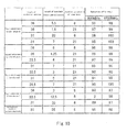
- Figure 10 is a table showing a length of each of the conductor antennas 110 to 310, a length of each of base bodies 120 and 220 in a longitudinal direction (its width and height are the same) and radiation efficiency obtained by changing a permittivity of the base body 220 obtained by changing a permittivity of the base bodies 120 and 220 in the antenna devices 100 to 400 in the first to fourth embodiments.
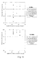
- Figure 11 is a diagram showing a relation between the radiation efficiency shown in Fig. 10 and the length of each conductor antenna. Moreover, as a comparative example, lengths, radiation efficiency and the like of the conventional chip antenna having a radiation electrode pattern are shown on the above same table. As is apparent from Figs.
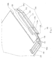
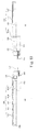
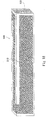
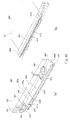
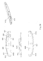
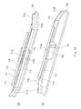
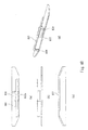
- Figures 12(a) and 12(b) are perspective views of examples embodying the antenna device 100 of the first embodiment.
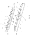
- Figures 13(a) and 13(b) are plan views of the examples embodying the antenna device 100 of the first embodiment.
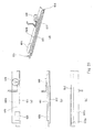
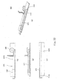
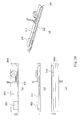
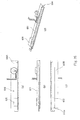
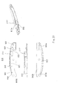
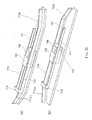
- Figures 14 (including 14[a], 14[b], and 14[c]) is a three-view drawing illustrating main portions of the antenna device of Fig. 12 .
- the antenna device 500 of the fourth embodiment includes a conductor antenna 510, a base body 520, a conductor line 530 (see Fig. 14[b] ), a power feeding connector 531, and a mounting hardware 532, all of which are mounted on a sub-board 540.
- the antenna device 500 is formed so as to be small-sized and to be thin and, therefore, besides a main board (not shown), the sub-board 540 can be provided.
- the sub-board 540 can be provided.
- some distance can be kept between the conductor antenna 510 and base body 520 and conducting portions such as an edge portion 550b (see Fig. 16 ), which serves as a grounding terminal, of the main board , the antenna made up of the conductor antenna 510 and base body 520 can operate in wide bands with high antenna gain obtained.
- the conductor antenna 510 is made up of a metal plate so as to be approximately U-shaped in which the conductor antenna 510 is folded so that a plane portion of a conductor 511 on one end side of the conductor antenna 510 shown in an upper portion of Fig. 12(b) is vertical with respect to a plane portion of a conductor 512 on the other end side of the conductor antenna 510 and a power feeding section 515 is formed in an end portion 511a of the conductor 511 on the one end side and an end portion 512a of the conductor 512 on the other end side is formed as an open end terminal.
- the base body 520 is made of a dielectric material or magnetic material so as to have a cuboid shape and is coupled between the end portion 511a of the conductor 511 on the one end side of the conductor antenna 510 and the open end portion 512a of the conductor 512 on the other end of the conductor antenna 510, that is, to the end portion 511a of the conductor 511 facing the conductor 512 and the end portion 512a of the conductor 512 facing the conductor 511, by using an adhesive, in a manner in which the base body 520 is sandwiched between the end portions 511a and 512a.
- FIG 17 is a perspective view of a modified example of the antenna device 100 of the first embodiment and, in Fig. 17 , same reference numbers are assigned to components corresponding to those in the first embodiment and their descriptions are omitted accordingly.
- the antenna device 600 of the modified example has no sub-board 540 on which a mounting hardware 532 is mounted.
- an end portion 511a of a conductor 511 on one end side of a conductor antenna 510 and a base body 520 are mounted directly on a main board 650 and the conductor 511 on the one end side of the conductor antenna 510 and a folded-back portion 514 of the conductor 512 on the other end of the conductor antenna 510 are also mounted directly on the main board 650.
- the same actions and effects as obtained by the above antenna device 500 can be achieved by the antenna device 600 of the modified example and, therefore, its handling is made easy at a time of assembling the antenna device 600 and the mobile phone having the antenna device 600 can maintain its strength even when receiving external force.
- the conductor antenna 510 can be secured stably to the sub-board 540.
- FIG. 18 is a perspective view of an antenna device of the sixth embodiment of the present invention, which is similar to an antenna device used in the sixth embodiment shown in Fig. 19 that is configured by lengthening a base body 620 and by printing all portions of conductors 611 and 612 on the base body 620 as a conductive film.
- the antenna device 900 of the sixth embodiment is so configured that its base body is made longer and a metal conductive film is printed on a surface of the base body 620 by using a screen printing method, deposition method, or a like and its conductor antenna 910 is formed so as to be approximately U-shaped.
- a shape of the metal conductive film can be selected, as appropriate, from a line shape, crank shape, meandering shape, helical shape, or a like.
- FIG. 19 is a diagram showing basic configurations of the antenna device of the sixth embodiment and Fig. 19(a) is a perspective view of the antenna device mounted on the sub-board and part of the main board viewed from a board and Fig. 19(b) is a perspective view of the antenna device mounted on the sub-board from a rear of part of the main board.
- Figure 20 is a diagram illustrating the antenna device 600 of the sixth embodiment and Fig. 20(a) is its plan view, Fig. 20(b) is its side view, Fig. 20(c) is its bottom plan view, Fig. 20(d) is its perspective view.
- the antenna device 600 includes a conductor antenna 610 and a base body 620, both of which are mounted on the sub-board 640.
- the conductor antenna 610 is configured so as to be approximately U-shaped in which the conductor antenna 610 is formed so that a plane portion of a conductor 611 on one end side of the conductor antenna 610 shown in an upper portion of Fig. 19(a) is vertical with respect to a plane portion of a conductor 612 on the other end side of the conductor antenna 610 and a power feeding section 615 is formed in an end portion 611a of the conductor 611 on the one end side and an end portion 612a of the conductor 612 on the other end side is formed as an open end terminal. That is, the conductors 611 and 612 are placed far from each other and between the conductors 611 and 612 is formed band-shaped space 613 and a folded-back portion 614.
- the conductor 611 on the one end side of the conductor antenna 610 is made up of a metal plate with a thickness of 0. 3 mm so as to be 32. 5 mm in length and, in order to reduce a resistance value to achieve high antenna gain and to minimize a loss, gold plating is given to its surface. More specifically, the conductor 611 is constructed of a plate metal made of bronze phosphate so as to be 32. 5 mm in length to form a long-length ⁇ -shaped profile and is mounted (in a stood state) so that the ⁇ -shaped concave portion forms band-shaped space 613 between the conductor 611 and the main surface 640A of the sub-board 640.
- the base body 620 is made of a dielectric material so as to have a cuboid shape and is surface-mounted on an end portion 640a of the main surface 640A of the sub-board 640.
- the base body 620 is made of ceramic, that provides a low loss in high frequencies, such as alumina, silica, magnesium, or a like so as to be 5. 5 mm x 3 m x 2 mm in size.
- the base body 620 may be made of not only a dielectric material but also a magnetic material.
- the magnetic material substance for the base body 620 Z-type or Y-type hexagonal ferrite called "planar" or composite materials containing these ferrite materials, or a like can be used.
- a sintered body of ferrite is used and, more preferably, Y-type ferrite is employed.
- the sintered body of ferrite has a high volume resistivity and is advantageous in terms of its insulation effects against a conductor. The use of ferrite having high volume resistivity makes it unnecessary to provide insulating coating against the conductor.
- Y-type ferrite can maintain its magnetic permeability in a high-frequency up to 1 GHz and a magnetic loss is small in a frequency up to 1 GHz.
- the sintered body of Y-type ferrite includes not only Y-type ferrite of a single phase but also ferrite of other phase such as Z-type ferrite, W-type ferrite, or a like.
- the base body 620 made of the magnetic material, as in the case of using the dielectric material, can be formed so as to have a cuboid shape and to be 5. 5 mm x 3 mm x 2 mm in size.
- the base body 620 is placed between the conductor 611 on one end side of the conductor antenna 610 and the conductor 612 on the other end side and its side surface 620B is coupled to the conductor 611 on the one end side of the conductor antenna 610. That is, on an end portion 640a of the main surface 640A on the sub-board 640 is surface-mounted the base body 620 and to its side surface 620B is coupled an end portion 611a of the conductor 611 on the one end side of the conductor antenna 610 by using an adhesive.
- an electrode may be formed by screen printing on a coupled face between the side surface 620B of the base body 620 and the end portion 611a of the conductor 611 on the one end side of the conductor antenna 610 and the electrode may be coupled to the end portion 611a by a soldering method.
- the conductor 612 on the other end side of the conductor antenna 610 is surface-mounted in a portion which faces the conductor 611 on a rear surface 640B on the sub-board 640 along a direction of a length of the sub-board 640. More specifically, the conductor 612 is made up of foil having a specified width and is formed on the rear surface 640B of the sub-board along the direction of a length of the sub-board 640.
- a ⁇ -shaped end portion (folded-back portion 614) placed on an opposite side to the end portion 611a, which has the long-length ⁇ -shaped profile, of the conductor 611 on the one end side of the conductor antenna 610 is extended up to the rear surface 640B of the sub-board 640 and is then bent and, on the bent end portion is formed the conductor 612 on the other end side of the conductor antenna 610, which causes the conductor 611 to be electrically connected to the conductor 612.
- the ⁇ -shaped end portion (folded-back portion 614) of the conductor 611 on the one side of the conductor antenna 610 may be folded on the main surface 640A, without being extended to the rear surface 640B side of the sub-board 640, and the folded portion may be connected to the foil conductor 612 on the other end side by using a through-hole electrode (not shown) formed in the sub-board 640.
- a through-hole electrode not shown
- either of one end portion or the other end portion of the conductor antenna 610 is constructed of a metal plate made of a metal conductive plate.
- an end portion opposite to the one end portion or to the other end portion of the conductor antenna 610 may be made of metal conductive foil such as copper foil as formed on the sub-board 640 or may be fabricated by printing a metal conductive film on the sub-board 640 by a screen printing method or deposition method.
- the conductor 612 on the other end side of the conductor antenna 610 is formed by sticking foil to the rear surface 640B, however, as in the case of the conductor 611 on the one end side, the conductor 612 may be formed by using a metal plate made of bronze phosphate. In this case, the conductor 612 may be formed by sticking a plane portion of the metal plate on the rear surface 640B. Also, the conductor 612 on the other end side of the conductor antenna 610 is made up of a metal plate and the conductor 611 may be formed by combining other materials, for example, by using a line material (metal conductive line) or a like. In this case, both the conductors 612 and 611 may be coupled via a through-hole electrode or may be electrically connected via a side face electrode formed on a side face of the board serving as a folded-back portion.
- the end portion 612 of the conductor 612 on the other end side of the conductor antenna 610 is extended toward a bottom portion of the base body 620 on the rear surface 640B on the sub-board 640.
- the end portion 612a of the conductor 612 on the other end side is coupled to the bottom portion of the base body 620 with a gap corresponding to a thickness of the sub-board 640 interposed between the end portion 612a and the bottom portion and the end portion 612a of the conductor 612 is capacitively coupled to the end portion 611a of the conductor 611 on the one end side.
- the end portion 611a of the conductor 611 on the one end side of the conductor antenna 610 is connected to a power feeding line 641 via a conductor line 630. Between the power feeding line 641 and the conductor line 630 is mounted an impedance matching circuit made up of a chip element 631 or a like.
- the main board 650 is made of a glass epoxy resin or a like and serves as a PCB to be embedded in a mobile phone being one of multi band type wireless communication apparatuses of the embodiment of the present invention.
- the antenna device 600 is configured so as to be small-sized and thin and, therefore, can be mounted on the sub-board 640 being very small compared with the main board 650.
- some distance can be kept between the conductor antenna 610 and base body 620 and the conductor portions and the edge portion 650b of the main board 650 serving as a grounding terminal and electrostatic capacity between the conductor antenna 610 and the ground on the main board 650 is reduced, which enables the conductor antenna 610 and base body 620 to operate as a wide-band and high-gain antenna.
- the sub-board 640 may be secured to the case of a mobile phone to be described by using the mounting hardware 532 shown in Figs. 12 to 14 .
- the antenna device 600 and its sub-board 640 are housed in a lower portion of the case or a like of the mobile phone to be described later.
- a microphone in many cases.
- the microphone 649 is mounted on the sub-board 640 and the conductor 611 on the one end side is formed in a stood manner in an end portion placed in a width direction being opposite to the microphone 649 on the main surface 640A on the sub-board 640 and the conductor 612 on the other end side is formed in an end portion placed opposite to the microphone 649 in a width direction of the sub-board 640.
- the conductor 612 on the other end side of the conductor antenna 610 is made of metal conductive foil or a metal conductive film that can provide a freedom of design for a shape in order to place the conductor apart from the microphone 649 or a like or to bypass an obstacle.
- work of mounting an antenna device or a microphone is managed according to a method being different from that used for manufacturing the main board, thus enabling a rationalization of mobile phone production and shortening manufacturing time.
- the conductor pattern 666 for adjusting the transmitting / receiving frequency is formed from an upper surface of the base body 620 toward one end side and by performing a machining process such as a process of shaving part of the conductor pattern 666 for adjusting the transmitting / receiving frequency or a like, it is made possible to adjust the transmitting / receiving frequency for the antenna device 601, particularly in the GSM band.
- Figure 22 is a diagram illustrating an antenna device of the second modified example of the antenna device of the sixth embodiment of the present invention.
- Figure 22(a) is its plan view
- Fig. 22(b) is its side view
- Fig. 22(c) is its bottom plan view
- Fig. 22(d) is its perspective view.
- a position is changed in which the conductor 611 (metal plate) on the one end side of the conductor antenna 610 mounted on one main face (surface) of the sub-board 640 is coupled to the conductor 612 (copper foil) on the other end side of the conductor antenna 610 mounted on the other main face (rear) of the sub-board 640.
- the conductor 611 on the one end side of the conductor antenna 610 may be coupled, by folding back the conductor 611 at a mid-point of the length of the sub-board 640 in a longitudinal direction, to the conductor 612 (copper foil) and the coupling is achieved sufficiently only if the conductor 611 on the one end side of the conductor antenna 610 is coupled to the conductor 612 on the other end side at a place where approximately U-shaped folding-back formed.
- changing a height of the conductor 612 on the board side which extends from a position in which the conductor 611 is coupled to the conductor 612 in a direction opposite to the power feeding side, the resonant frequency in the GSM band can be calibrated.
- Figure 23 is a diagram illustrating an antenna device of the third modified example of the antenna device of the sixth embodiment of the present invention and Fig. 23(a) is its plan view, Fig. 23(b) is its side view, Fig. 23(c) is its bottom plan view and Fig. 23(d) is its perspective view.
- approximately half of a conductor 611 (metal plate) on one end side of a conductor antenna 610 mounted on one main face (surface) of a sub-board 640 and placed on a folded-back side from a conductor 612 on the other end side of the conductor antenna 610 is formed so that its plane portion is orthogonal to a main face of the sub-board 640 and approximately half of the conductor 611 placed on a power feeding side bypasses so that its plane portion is coupled to an upper face of the base body 620.
- an end portion 611a on the power feeding side faces in parallel to an end portion 612a of the conductor 612 on the other side of the conductor antenna 610 with the base body 620 being interposed between the end portion 611a and the end portion 612a and, therefore, by changing a distance between surfaces being in parallel to each other, a capacity between the end portion 611a and end portion 612a can be increased or decreased. This allows easy adjustment of transmittance / receiving frequencies.
- Figure 24 is a diagram illustrating an antenna device of the fourth modified example of the antenna device of the sixth embodiment of the present invention and Fig. 24(a) is its plan view, Fig. 24(b) is its side view, Fig. 24(c) is its bottom plan view and Fig. 24(d) is its perspective view.
- the conductor 612 on the other end side of the conductor antenna 610 is formed so as to be L-shaped or ⁇ -shaped on a rear of the sub-board 640 and, as a result, some distance is kept between an end portion of the rear of the sub-board 640 in a width direction and the conductor 612. This causes an increase in length of the conductor 612 on the other end side of the conductor antenna 610 and addition of its inductance and, therefore, the transmitting / receiving frequency can be easily adjusted.
- power is supplied from a transmitting / receiving section (not shown) mounted on the main board 650 through the power feeding line 641 and the conductor line 630 to the power feeding portion 615 from which power is then fed to the conductor antenna 610.
- an impedance matching circuit made up of chip elements or a like is mounted between the power feeding line 641 and the conductor line 630.
- power may be fed to the conductor 612 of the conductor antenna 610 formed on a rear of the sub-board 640.
- the conductor 611 to which the power feeding section is connected makes up a conductor on one end side of the conductor antenna 610 and the conductor 612 whose another end portion forms an open end terminal makes up the conductor on the other end side.
- the conductor 612 to which the power feeding section is connected makes up the conductor on the one end side and the conductor 611 whose end portion forms an open end terminal makes up the conductor on the other end side. Therefore, the end portion 611a of the conductor 611 connected to a side face 620B of the base body 620 makes up the open end terminal.
- FIG. 27 is a diagram illustrating an antenna device of the seventh modified example of the antenna device of the sixth embodiment of the present invention.
- a conductor antenna 610 includes a conductor 611 on one end side of the conductor antenna 610, a conductor 612 on the other end side of the conductor antenna 610, a base body 620, a power feeding connector 531, an impedance matching circuit 632 made up of chip elements, and a conductor line 630, all of which are mounted on a sub-board 640.
- An end portion 611a on the one end of the conductor 611 is connected to a power feeding electrode 615' formed on the base body 620 by a printing method and makes up a power feeding portion 615.
- An end portion 611a of the conductor 611 on the one end side is connected to a folded-back portion 614 and to the conductor 612 on the other end side via a through hole conductor to the sub-board 640.
- the conductor 612 on the other end side of the conductor antenna 610 is printed, as a conductive film, on a rear 640B of the sub-board 640 and end portions 612a and 612b of the conductor 612 on the other end side of the conductor antenna 610 operates as open end terminals.
- An entire profile of the electrode of the conductor antenna 610 is approximately U-shaped, which is formed by the conductor 611 on the one end side, folded-back portion 614, and conductor 612 on the other end side, with the sub-board 640 being interposed among these components wherein the end portion 612b of the conductor 612 on the other end side of the conductor antenna 610 extends from the folded-back portion 614 slightly up to the outside. That is, the conductors 611 and 612 are placed apart from each other with the sub-board 640 being interposed between the conductors 611 and 612.
- the conductor 610 when viewed from the sub-board 640, is placed, in an arc-shaped form, in a position on a case side in an upper portion of the sub-board 640 and is connected via a through-hole 643 passing through a main face 640A of the sub-board 640 to the conductor 612 on the other end side formed on a rear 640B and is placed (in a stood manner). Power is fed from the power feeding connector 631 via a conductor line on the sub-board 640 and matching circuit 632 to the power feeding section 615 from which power is further fed to the conductor antenna 610.
- Figure 28 is a diagram illustrating an antenna device of the eighth modified example of the antenna device of the sixth embodiment of the present invention.
- a conductor antenna 610 includes a conductor 611 placed on one end side of the conductor antenna 610, a conductor 612 on the other end side, a base body 620, a power feeding connector 631, an impedance matching circuit 632 made up of chip elements, and a conductor line 630, all of which are mounted on a sub-board 640.
- An end portion 611a of the conductor 611 on the one end side of the conductor antenna 610 is connected to a power feeding electrode 615' printed on the base body 620 and makes up a power feeding portion 615 through the base body 620.
- Another end portion of the conductor 611 is connected to the folded-back portion 614 and is further connected to the conductor 612 on the other end side via the through hole formed on the sub-board 640.
- On a rear 640B of the sub-board 640 is printed, as a conductive film, the conductor 612 on the other end side of the conductor antenna 610 and end portions 612a and 612b on the other end side operate as open end terminals.
- An entire profile of the electrode of the conductor antenna 610 is approximately U-shaped, which is formed by the conductor 611, folded-back portion 614, and conductor 612, with the sub-board 640 being interposed among these components and the end portion 612b of the conductor 612 extends from the folded-back portion 614 slightly up to the outside.
- the configurations of the conductor antenna 610 differ from those of others in that the conductor 611, after being folded toward an upper face of the board 640 so as to have a crank-shaped profile at a mid-point of the length of the conductor 611, is connected to the folded-back portion 614.
- the conductors 611 and 612 are placed far from each other with the sub-board 640 being interposed between the conductors 611 and 612 and band-shaped space is formed between the conductors 611 and 612, which also shows an example in which the profile of this portion can be changed depending on a shape of surrounding components, case, or a like.
- the conductor 610 when viewed from the sub-board 640, is placed (in a stood manner), in an arc-shaped form, in a position on a case side in an upper portion of the sub-board 640 and is connected via a through-hole 643 passing through a main face 640A of the sub-board 640 to the conductor 612 formed on a rear 640B.
- Power is fed from the power feeding connector 631 via a conductor line on the sub-board 640 and matching circuit 632 to the power feeding section 615 from which power is further fed to the conductor antenna 610.
- Figure 29 is a diagram illustrating an antenna device of the ninth modified example of the antenna device of the sixth embodiment of the present invention ((In Fig. 29 , since the configurations are the same as explained in the modified example 7, same reference numbers as shown in the modified example 7 are assigned).
- a conductor antenna 610 includes a conductor 611 on one end side of the conductor antenna 610, a conductor 612 on the other end side of the conductor antenna 610, a base body 620, a power feeding connector 631, an impedance matching circuit made up of chip elements, and a conductor line 630, all of which are mounted on a sub-board 640.
- An end portion 611a of the conductor 611 on the one end side of the conductor antenna 610 is connected to a power feeding electrode 615' formed on the board 620 by a printing method and makes up a power feeding portion.
- Another end portion of the base body 611 is connected to a folded-back portion 614 and is further connected to the conductor 612 on the other end side via a through-hole formed on the sub-board 640.
- On a rear 640B of the sub-board 640 is printed the conductor 612 on the other end side as a conductive film and end portions 612a and 612b on the other end side operate as open end terminals.
- An entire profile of the electrode of the conductor antenna 610 is approximately U-shaped, which is formed by the conductor 611, folded-back portion 614, and conductor 612, with the sub-board 640 being interposed among these components and the end portion 612b of the conductor 612 extends from the folded-back portion 614 slightly up to the outside.
- Configurations of the conductor antenna 610 differ from others in that a supporting portion 611b extends from a mid-point of the length of the conductor 611 toward an upper face of the sub-board 640 to support the conductor 611 and is placed on the sub-board 640 in a stood manner.
- the portion to support the conductor 611 is increased, which can achieve an antenna device with high mechanical strength and can increase convenience at a time of assembling the antenna device.
- the base body 620 is placed on the sub-board 640 and is coupled to the conductor 611.
- the sub-board 640 has a specified permittivity, in the case of a frequency band not requiring such a permittivity as the base body 620 has or in the case of having comparatively large antenna space, the use of the base body 620 is not necessary and, as a portion equivalent to the base body, the sub-board 640 or the main board 650 can be considered as an insulating material, that is, a dielectric material, which enables reduction in component counts leading to low costs, thus further miniaturization of the antenna device.
- Figure 31 is also a diagram showing an example in which the antenna device of the sixth embodiment is applied to a mobile phone in which the power feeding route other than the antenna device, microphone, or a like in the mobile phone are shown in particular.
- a case 10 of the mobile phone is housed a metal portion (not shown) on a case side, which is slightly smaller than the case 10.
- a main board 650 is placed in an upper half area in Fig. 30(a) viewed from a rear side of the mobile phone and the battery 12 is placed in a lower half area in Fig. 30(a) and the antenna device 600 or a like are placed in a lower end in Fig. 30(a) .
- Fig. 30(a) As shown in Fig.
- a power feeding port 659 mounted in a central portion on one end side of the main board 650 through a power feeding line 641 and conductor line 630 to a power feeding section 615 (see Fig. 19 ).
- a flexible board 651 for a number button of a mobile phone is placed in upper and lower areas in Fig. 30(b) viewed from a keypad side of the mobile phone and the antenna device 600, microphone 649 (see Fig. 31 ) or a like are placed in a lower end in Fig. 30(b) (see Fig. 31 ).
- the conductor antenna 610 and base body 620 By configuring as above, distance between the conductor antenna 610 and base body 620 and metal portions such as a battery 12, microphone 649, flexible board 651, or a like is kept physically and electrically (for example, no dielectric exists between the conductor antenna and the ground) and, therefore, capacitive components between the conductor antenna 610 and a ground of the flexible board 651 or a like are reduced, thereby making the conductor antenna 610 and base body 620 be a wide-band and high-gain antenna. That is, according to the embodiment, by placing the antenna device 600 far from the metal portions existing near to the antenna including the flexible board 651, battery 12, microphone 649, or a like, the high-gain of the antenna device is obtained.
- FIG. 32 is a diagram showing basic configurations of the antenna device of the seventh embodiment of the present invention and is a perspective view in which the antenna device mounted on the board and part of the board are seen from a surface of the board.
- Figure 33(a) is a perspective view of the antenna device shown in Fig. 32 seen from a front side.
- Figure 33(b) is a diagram of the antenna device of the first modified example of the seventh embodiment in which a position of a folded-back portion of the conductor 710 shown in Fig. 32 and 32(a) is changed so as to be reversed to each other, which is seen from a rear side of the board.
- FIG. 32 is approximately orthogonal to a plane portion of the conductor 712 on the other end side in a lower portion in Fig. 32 and, in the conductor 711 on the one end side is mounted a power feeding section 715 and an end portion 712a of the conductor 712 on the other end side operates as an open end terminal. That is, the conductors 711 and 712 are placed far from each other, and between the conductors 711 and 712 is formed band-shaped space.
- the conductor 711 on one end side of the conductor antenna 710 and the conductor 712 on the other end side are fabricated by a metal plate (metal conductive plate) and, in order to decrease a resistance, to achieve high gain, and to reduce a loss, gold plating is given to their surfaces.
- the conductor antenna 710 is constructed of a metal plate made of bronze phosphate so as to be approximately U-shaped and an approximately central portion of the conductor 711 on one end side of the conductor antenna 710 is coupled to an upper face of the base body 720 and an approximately central portion of the conductor 712 on the other end side is coupled to a side face of the base body 720 and is mounted in a tip portion 755 of the main face (surface) 750 on the main-board 750.
- An approximately central portion 711b of the conductor 711 on the one end side is placed on an upper face of the base body 720 and an approximately central portion 712b of the conductor 712 is coupled to a side face of the base body 720 by an adhesive.
- the electrode may be coupled to the conductor antenna 710 by means of soldering (that is, approximately central portion between an approximately central portion of the conductor 711 on the one side and an approximately central portion of the conductor 712 on the other end side).
- the base body 720 is made of a dielectric material and formed so as to have a cuboid shape and is surface-mounted in a central portion of the tip portion 755 of the main face (surface) 750A of the main board 750 in a width direction.
- the base body 720 is made of ceramic, that provides a low loss in high frequencies, such as alumina, silica, magnesium, or a like and is configured so as to be 5. 5 mm x 3 mm x 2 mm in size.
- the base body 720 is made of at least either of a dielectric material or magnetic material and is formed to have a cuboid shape and is coupled to an approximately central portion 711b of the conductor 711 on the one end side of the conductor antenna 710 and to a central portion 712b of the conductor 712 on the other end side of the conductor antenna 710, that is, to the central portions 711b and central portion 712a of the conductors 711 and 712 both facing each other.
- the conductor 712 on the other end side of the conductor antenna 710 is capacitively coupled to the central portion 711b on the one end side of the conductor 711 with the base body 720 being interposed between the conductors 711 and 712.
- Figure 38 is a diagram illustrating an entire main board 750 of a mobile phone on which the antenna device 700 of the seventh embodiment is mounted. Power is fed from a transmitting / receiving circuit (not shown) mounted on the main board 750 through the power feeding line 741 to the conductor antenna 710 placed far from the transmitting / receiving circuit.
- the antenna device 700 is configured to be small-sized and to be three-dimensional with respect to a board surface and, therefore, can be made thin in a direction of the board surface and can be placed on a side far from a tip portion 755 of the main face (surface) 750A of the main board 750 and far from a ground of the main board 750.
- a corner of the tip portion 755 of the main face (surface) 750A of the main board 750 is chamfered in a manner to match with a shape of a lower portion of a case of a mobile phone into which the antenna device 700 is embedded and, therefore, corresponding extended portions 712A and 712B of both ends of the conductor 712 on the other side of the conductor antenna 710 are bent so that the conductor 712 can match with the shape.
- the plane portion of the conductor 711 on one end side of the conductor antenna 710 in an upper portion in Figs. 32 and 33 is approximately orthogonal to the plane of the conductor 712 on the other end side of the conductor antenna 710, however, in the antenna devices 700 of the second and third modified examples, as shown in Figs. 34(a) and 34(b) , a plane portion of the conductor 711 facing the conductor 712 on the one end side is parallel to a plane portion of the conductor 712 on the other end side with the base body 720 interposed between the conductors 711 and 712.
- the conductor antenna 710 is configured so as to be approximately U-shaped and the plane portion of the conductor 711 on the one end side is parallel to the plane portion of the conductor 712 with the base body 720 being interposed between the conductors 711 and 712 and in the conductor 711 on the one end side is formed the power feeding section 715 and the end portion 712a of the conductor 712 on the other end side operates as an open end terminal.
- the conductors 711 and 712 are placed far from each other and between the conductors 711 and 712 is formed band-shaped space 713.
- Both the conductor 711 on one end side of the conductor antenna 710 and the conductor 712 on the other end side are fabricated by a metal plate (metal conductive plate) and, in order to decrease a resistance, to achieve high gain, and to reduce a loss, gold plating is given to their surfaces.
- the conductor antenna 710 is constructed of a metal plate made of bronze phosphate being 0.3 mm in thickness so as to be approximately U-shaped and an approximately central portion of the conductor 711 on one end side of the conductor antenna 710 is coupled to a side face 720 on the other side and an approximately central portion of the conductor 712 on the other end side is coupled to a another side face 720B facing the side face 720A of the base body 720 and is placed on a tip portion 755 of the main face (surface) 750A of the main board 750.
- the approximately central portion 711b of the conductor 711 on the one end side is coupled to a side face 720A of the base body 720 on the other end side by using an adhesive and the approximately central portion is coupled to a side face 720B of the base body 720 by using the adhesive.
- the electrode may be coupled to the conductor antenna 710 by means of soldering (that is, approximately central portion between an approximately central portion of the conductor 711 on the one side and an approximately central portion of the conductor 712 on the other end side).
- the conductor antenna 710 is connected to the power feeding line 741 through the conductor line 730.
- power is fed from a transmitting / receiving circuit (not shown) mounted in the main board 750 through the power feeding line 741 to the conductor antenna 710.
- a transmitting / receiving circuit (not shown) mounted in the main board 750 through the power feeding line 741 to the conductor antenna 710.
- an impedance matching circuit made up of a chip element or a like.
- Figure 35(a) shows the antenna device of the fourth modified example of the seventh embodiment, which is a perspective view of the antenna device seen from a front side.
- Figure 35(a) is a perspective view in which a position of a folded-back portion of the conductor 710 shown in Fig. 35(a) is changed so as to be reversed to each other, which is seen from a rear side.
- the plane portion of the conductor 711 on the one end side of the conductor antenna 710 facing the conductor 720 is parallel to the plane of the conductor 712 on the other end side with the base body 720 being interposed between the two plane portions and, additionally, to the base body 720 is connected the conductor 711 on the one end side of the conductor antenna 710, which provides a conductor pattern 766 enabling the adjustment of transmitting / receiving frequency.
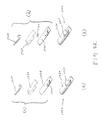
- the number (1) shows, as a parameter, a length of a bent portion of an extended portion 712A of the conductor 712 on the other end side
- the number (2) shows a length of a bent portion of an extended portion 712B of the conductor 712 on the other end side
- the number (3) shows a length of the conductor 711 on one end side
- the number (4) shows, as a parameter, a width of the conductor 711 on the one end side
- the number (5) shows a position of a folded-back portion of the conductive antenna 710 formed so as to be approximately U-shaped.
- Figure 38 is a diagram illustrating an entire main board of a mobile phone on which the antenna device of the seventh embodiment is mounted.
- the power feeding port 759 from which power is fed through the power feeding line 741 and conductor line 730 to the conductor antenna 710 and the base body 720.
- power may be fed by connecting a connector mounted on the main board 750 to a power feeding connector (not shown) mounted on the tip portion 755 of the main board 750 through a coaxial cable for power feeding.
- the antenna device 800 has a conductor 810, a base body 820, and a conductor line 830 (not shown), all of which are mounted on a tip portion of a main face (surface) of the main board.
- the conductor antenna 810 is configured so as to be approximately U-shaped and so that a plane portion of the conductor 811 on one end side of the conductor antenna 810 in an upper portion in Fig. 39 is in parallel to a plane portion of the conductor 812 facing the conductor 811 on the other end side in a lower portion in Fig. 39 .
- a central portion 811b of the conductor 811 on the one end side of the conductor antenna 810 is coupled to an upper face of the conductor 820 and is connected through a folded-portion 814 to the conductor 812 on the other end side.
- the conductor 812 on the other end side is made of metal conductive foil on a rear of a tip portion 855 on the board.
- a power feeding section 815 is connected to the conductor 811 on the one end side and an end portion of the conductor 812 on the other end side operates as an open end terminal. That is, the conductors 811 and 812 are placed far from each other and band-shaped space 813 is interposed between the conductors 811 and 812. Thereby, the band-shaped space 813 is formed.
- the conductor 811 on one end side of the conductor antenna 810 is constructed of a metal plate (metal conductive plate) made of, for example, bronze phosphate with a thickness of 0. 3 mm and, in order to reduce a resistance value to obtain a high antenna gain and to minimize a loss, gold plating or silver plating is given on a surface of the conductor 811.
- a metal plate metal conductive plate
- bronze phosphate with a thickness of 0. 3 mm and, in order to reduce a resistance value to obtain a high antenna gain and to minimize a loss, gold plating or silver plating is given on a surface of the conductor 811.
- the conductor 812 on the other end side of the conductor antenna 810 is mounted on a rear of the tip portion 855 of the board and more specifically the conductor 812 is made of copper foil having a specified width which extends along a chamfered outer edge on a rear of the tip portion 855 of the board.
- the conductor 812 on the other end side of the conductor antenna 810 is made of copper foil, however, alternatively, may be constructed of a metal plate made of bronze phosphate as in the case of the conductor 811 on the one end side of the conductor antenna 810. In this case, a plane portion of the metal plate may be adhered to a rear of the tip portion 855 of the board.
- a central portion 812b of the conductor 812 on the other end side of the conductor antenna 810 extends over a bottom face portion of the base body 820 and, as a result, the central portion 812b of the conductor 812 on the other end side is coupled to a bottom face of the base body 820 with a distance corresponding to a thickness of the tip portion 855 of the board being interposed between the central portion 812 and the bottom face of the base body 820 and is capacitively coupled to a central portion 811b of the conductor 811 on the one end side with the base body 820 interposed between the central portion 812b and the central portion 811b.
- a conductor pattern 866 to be used for adjusting capacitive coupling to the conductor 811 on the other end side of the conductor antenna 810 is formed on the base body 820. That is, over a side face through a bottom face of the conductor 820, the conductor pattern 866 for adjusting capacitive coupling is formed and, by performing a machining process such as a process of shaving part of the conductor pattern 866, a degree of the capacitive coupling to the conductor 811 can be changed, which enables the adjustment of transmitting / receiving frequency in the GSM band in the antenna device 800.
- the conductor 812 (foil or a like) on the other end side on the rear of the main board 850 may be connected to the conductor 812 (foil or a like) on the one end side and the conductor 811(metal plate) on the other side.
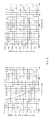
- Figure 41 shows results of measurement of an antenna radiation pattern (gain directivity) obtained when power is fed from an end portion of the board on which the antenna is mounted and when power is fed from a central portion of the board on which the antenna is mounted.
- Figure 41(a) shows the antenna radiation pattern observed when power was fed from the end portion of the antenna-mounted board.
- Figure 41(b) shows the antenna radiation pattern observed when power is fed from the central portion of the antenna-mounted board.
- Numeric values of 5, -5, -15, -25, and -35 represent gains [dBi] and numeric values of 0, 30, 60, ⁇ , 330 represent azimuth angles. The measurement was made at frequencies of 1. 91 GHz. As shown in Figs.
- the antenna radiation pattern shows a characteristic of being a uniform circle, which can provide uniform directivity, that is, an excellent gain.
Landscapes
- Engineering & Computer Science (AREA)
- Computer Networks & Wireless Communication (AREA)
- Support Of Aerials (AREA)
- Waveguide Aerials (AREA)
- Details Of Aerials (AREA)
- Variable-Direction Aerials And Aerial Arrays (AREA)
Applications Claiming Priority (3)
| Application Number | Priority Date | Filing Date | Title |
|---|---|---|---|
| JP2006107177 | 2006-04-10 | ||
| JP2006220792 | 2006-08-12 | ||
| EP07104706A EP1845582B1 (de) | 2006-04-10 | 2007-03-22 | Breitbandige Antenne mit einem U-förmigen Antennenleiter |
Related Parent Applications (1)
| Application Number | Title | Priority Date | Filing Date |
|---|---|---|---|
| EP07104706.2 Division | 2007-03-22 |
Publications (1)
| Publication Number | Publication Date |
|---|---|
| EP2204881A1 true EP2204881A1 (de) | 2010-07-07 |
Family
ID=38008086
Family Applications (2)
| Application Number | Title | Priority Date | Filing Date |
|---|---|---|---|
| EP07104706A Not-in-force EP1845582B1 (de) | 2006-04-10 | 2007-03-22 | Breitbandige Antenne mit einem U-förmigen Antennenleiter |
| EP10156367A Withdrawn EP2204881A1 (de) | 2006-04-10 | 2007-03-22 | Breitbandige Antenne mit einem U-förmigen Antennenleiter |
Family Applications Before (1)
| Application Number | Title | Priority Date | Filing Date |
|---|---|---|---|
| EP07104706A Not-in-force EP1845582B1 (de) | 2006-04-10 | 2007-03-22 | Breitbandige Antenne mit einem U-förmigen Antennenleiter |
Country Status (6)
| Country | Link |
|---|---|
| US (1) | US7679569B2 (de) |
| EP (2) | EP1845582B1 (de) |
| KR (1) | KR20070101168A (de) |
| CN (1) | CN101055940B (de) |
| AT (1) | ATE468626T1 (de) |
| DE (1) | DE602007006584D1 (de) |
Cited By (1)
| Publication number | Priority date | Publication date | Assignee | Title |
|---|---|---|---|---|
| CN106374196A (zh) * | 2016-11-16 | 2017-02-01 | 西安电子科技大学 | 基于人工电磁材料的高增益低剖面环槽天线 |
Families Citing this family (16)
| Publication number | Priority date | Publication date | Assignee | Title |
|---|---|---|---|---|
| CN101461096B (zh) * | 2006-05-31 | 2013-05-29 | 日立金属株式会社 | 天线装置及使用该天线装置的无线通信设备 |
| JP5221115B2 (ja) * | 2007-11-30 | 2013-06-26 | 三菱電線工業株式会社 | アンテナ装置 |
| JP5018946B2 (ja) | 2009-10-13 | 2012-09-05 | ソニー株式会社 | アンテナ |
| US8644894B2 (en) * | 2010-03-12 | 2014-02-04 | Blackberry Limited | Mobile wireless device with multi-band antenna and related methods |
| JP5796699B2 (ja) * | 2010-11-12 | 2015-10-21 | 戸田工業株式会社 | 折返しダイポールアンテナ、該折返しダイポールアンテナを用いたrfタグ |
| KR101485569B1 (ko) * | 2014-01-22 | 2015-01-22 | 광운대학교 산학협력단 | 금속 덮개가 적용된 이동통신 단말기의 nfc 안테나 |
| US9203141B1 (en) | 2014-06-11 | 2015-12-01 | King Slide Technology Co., Ltd. | Communication device and antenna thereof |
| EP2958189B1 (de) * | 2014-06-20 | 2023-05-31 | King Slide Technology Co., Ltd. | Kommunikationsvorrichtung und Antenne dafür |
| US9520646B1 (en) * | 2014-06-21 | 2016-12-13 | Redpine Signals, Inc. | Dual-band compact printed circuit antenna for WLAN use |
| JP6319801B2 (ja) * | 2014-08-06 | 2018-05-09 | アルプス電気株式会社 | 無線通信装置 |
| US10027035B2 (en) | 2014-09-30 | 2018-07-17 | Skyworks Solutions, Inc. | Modified Z-type hexagonal ferrite materials with enhanced resonant frequency |
| US10032547B2 (en) | 2014-10-24 | 2018-07-24 | Skyworks Solutions, Inc. | Increased resonant frequency alkali-doped Y-phase hexagonal ferrites |
| USD824885S1 (en) * | 2017-02-25 | 2018-08-07 | Airgain Incorporated | Multiple antennas assembly |
| TWI638486B (zh) * | 2017-10-27 | 2018-10-11 | 廣達電腦股份有限公司 | 行動裝置 |
| CN111653861B (zh) * | 2019-03-04 | 2021-12-17 | 上海安费诺永亿通讯电子有限公司 | 一种天线与通讯设备壳体的一体化结构及制备方法 |
| KR102731105B1 (ko) * | 2020-05-14 | 2024-11-18 | 삼성전자주식회사 | 전자 장치 및 전자 장치의 안테나 제어 방법 |
Citations (9)
| Publication number | Priority date | Publication date | Assignee | Title |
|---|---|---|---|---|
| JPH03502157A (ja) | 1988-04-11 | 1991-05-16 | モトローラ・インコーポレーテッド | バランス式薄型ハイブリッド・アンテナ |
| WO1999028990A1 (en) | 1997-12-01 | 1999-06-10 | Kabushiki Kaisha Toshiba | Multifrequency inverted f-type antenna |
| US6342860B1 (en) * | 2001-02-09 | 2002-01-29 | Centurion Wireless Technologies | Micro-internal antenna |
| US20030132883A1 (en) * | 2002-01-16 | 2003-07-17 | Accton Technology Corporation | Surface-mountable dual-band monopole antenna for WLAN application |
| JP2004007803A (ja) | 2003-07-28 | 2004-01-08 | Nec Saitama Ltd | アンテナ装置 |
| WO2004042866A1 (en) * | 2002-11-08 | 2004-05-21 | Eung-Soon Chang | Folded monopole antenna for cellular phone |
| JP2004363789A (ja) | 2003-06-03 | 2004-12-24 | Sharp Corp | 逆fアンテナ |
| JP2005229365A (ja) | 2004-02-13 | 2005-08-25 | Matsushita Electric Ind Co Ltd | チップアンテナ |
| WO2006070233A1 (en) * | 2004-12-31 | 2006-07-06 | Nokia Corporation | Internal multi-band antenna with planar strip elements |
Family Cites Families (8)
| Publication number | Priority date | Publication date | Assignee | Title |
|---|---|---|---|---|
| JP3457351B2 (ja) * | 1992-09-30 | 2003-10-14 | 株式会社東芝 | 携帯無線装置 |
| JP3502157B2 (ja) | 1994-07-18 | 2004-03-02 | 東京エレクトロン株式会社 | プラズマ処理装置 |
| US5644319A (en) * | 1995-05-31 | 1997-07-01 | Industrial Technology Research Institute | Multi-resonance horizontal-U shaped antenna |
| US6031503A (en) * | 1997-02-20 | 2000-02-29 | Raytheon Company | Polarization diverse antenna for portable communication devices |
| EP1258945A3 (de) * | 2001-05-16 | 2003-11-05 | The Furukawa Electric Co., Ltd. | Linienförmige Antenne |
| JP3660623B2 (ja) * | 2001-07-05 | 2005-06-15 | 株式会社東芝 | アンテナ装置 |
| JP2004104419A (ja) * | 2002-09-09 | 2004-04-02 | Hitachi Cable Ltd | 携帯無線機用アンテナ |
| US7286090B1 (en) * | 2006-03-29 | 2007-10-23 | Hong Kong Applied Science And Technology Research Institute Co., Ltd. | Meander feed structure antenna systems and methods |
-
2007
- 2007-03-22 DE DE602007006584T patent/DE602007006584D1/de active Active
- 2007-03-22 US US11/723,878 patent/US7679569B2/en not_active Expired - Fee Related
- 2007-03-22 AT AT07104706T patent/ATE468626T1/de not_active IP Right Cessation
- 2007-03-22 EP EP07104706A patent/EP1845582B1/de not_active Not-in-force
- 2007-03-22 EP EP10156367A patent/EP2204881A1/de not_active Withdrawn
- 2007-04-10 KR KR1020070035255A patent/KR20070101168A/ko not_active Ceased
- 2007-04-10 CN CN2007100960449A patent/CN101055940B/zh not_active Expired - Fee Related
Patent Citations (10)
| Publication number | Priority date | Publication date | Assignee | Title |
|---|---|---|---|---|
| JPH03502157A (ja) | 1988-04-11 | 1991-05-16 | モトローラ・インコーポレーテッド | バランス式薄型ハイブリッド・アンテナ |
| WO1999028990A1 (en) | 1997-12-01 | 1999-06-10 | Kabushiki Kaisha Toshiba | Multifrequency inverted f-type antenna |
| US6342860B1 (en) * | 2001-02-09 | 2002-01-29 | Centurion Wireless Technologies | Micro-internal antenna |
| US20030132883A1 (en) * | 2002-01-16 | 2003-07-17 | Accton Technology Corporation | Surface-mountable dual-band monopole antenna for WLAN application |
| WO2004042866A1 (en) * | 2002-11-08 | 2004-05-21 | Eung-Soon Chang | Folded monopole antenna for cellular phone |
| JP2004363789A (ja) | 2003-06-03 | 2004-12-24 | Sharp Corp | 逆fアンテナ |
| JP2004007803A (ja) | 2003-07-28 | 2004-01-08 | Nec Saitama Ltd | アンテナ装置 |
| JP2005229365A (ja) | 2004-02-13 | 2005-08-25 | Matsushita Electric Ind Co Ltd | チップアンテナ |
| WO2006070233A1 (en) * | 2004-12-31 | 2006-07-06 | Nokia Corporation | Internal multi-band antenna with planar strip elements |
| EP1856764A1 (de) * | 2004-12-31 | 2007-11-21 | Nokia Corporation | Interne mehrband-antenne mit planaren streifenelementen |
Cited By (2)
| Publication number | Priority date | Publication date | Assignee | Title |
|---|---|---|---|---|
| CN106374196A (zh) * | 2016-11-16 | 2017-02-01 | 西安电子科技大学 | 基于人工电磁材料的高增益低剖面环槽天线 |
| CN106374196B (zh) * | 2016-11-16 | 2019-03-26 | 西安电子科技大学 | 基于人工电磁材料的高增益低剖面环槽天线 |
Also Published As
| Publication number | Publication date |
|---|---|
| US7679569B2 (en) | 2010-03-16 |
| CN101055940A (zh) | 2007-10-17 |
| KR20070101168A (ko) | 2007-10-16 |
| DE602007006584D1 (de) | 2010-07-01 |
| EP1845582B1 (de) | 2010-05-19 |
| ATE468626T1 (de) | 2010-06-15 |
| US20070290944A1 (en) | 2007-12-20 |
| CN101055940B (zh) | 2013-03-13 |
| EP1845582A1 (de) | 2007-10-17 |
Similar Documents
| Publication | Publication Date | Title |
|---|---|---|
| EP1845582B1 (de) | Breitbandige Antenne mit einem U-förmigen Antennenleiter | |
| KR101007529B1 (ko) | 안테나 장치 및 통신기기 | |
| US7403164B2 (en) | Multi-band monopole antenna for a mobile communications device | |
| JP4868128B2 (ja) | アンテナ装置及びそれを用いた無線通信機器 | |
| JP4284252B2 (ja) | 表面実装型アンテナおよびそれを用いたアンテナ装置ならびに無線通信装置 | |
| EP1750323A1 (de) | Mehrbandantennenvorrichtung für ein Funkkommunikationsendgerät, und Funkkommunikationsendgerät mit einer solchen Mehrbandantennenvorrichtung | |
| KR101027089B1 (ko) | 표면실장형 안테나 및 안테나 장치 | |
| JP2002185231A (ja) | 小型マイクロ波アンテナ | |
| WO2005109569A1 (ja) | マルチバンドアンテナ、回路基板および通信装置 | |
| JP2001352212A (ja) | アンテナ装置およびそれを用いた無線装置 | |
| JP2003188624A (ja) | 指向性アンテナ | |
| US20060290575A1 (en) | Antenna integrated into a housing | |
| JP4263972B2 (ja) | 表面実装型アンテナおよびアンテナ装置ならびに無線通信装置 | |
| JPH10247806A (ja) | 携帯無線機用アンテナおよびそれを用いた携帯無線機 | |
| WO2004025781A1 (ja) | ループアンテナ | |
| EP2028717B1 (de) | Mehrbandantennenanordnung angeordnet auf einem dreidimensionalen Substrat | |
| TW200402905A (en) | Multiband microwave antenna | |
| JP5061689B2 (ja) | アンテナ装置及びそれを用いたマルチバンド型無線通信機器 | |
| JPH09232854A (ja) | 移動無線機用小型平面アンテナ装置 | |
| JP3964919B2 (ja) | アンテナ装置 | |
| JP2007524322A (ja) | アンテナアレイ | |
| JP2006050212A (ja) | チップアンテナ |
Legal Events
| Date | Code | Title | Description |
|---|---|---|---|
| PUAI | Public reference made under article 153(3) epc to a published international application that has entered the european phase |
Free format text: ORIGINAL CODE: 0009012 |
|
| AC | Divisional application: reference to earlier application |
Ref document number: 1845582 Country of ref document: EP Kind code of ref document: P |
|
| AK | Designated contracting states |
Kind code of ref document: A1 Designated state(s): AT BE BG CH CY CZ DE DK EE ES FI FR GB GR HU IE IS IT LI LT LU LV MC MT NL PL PT RO SE SI SK TR |
|
| 17P | Request for examination filed |
Effective date: 20110105 |
|
| STAA | Information on the status of an ep patent application or granted ep patent |
Free format text: STATUS: THE APPLICATION IS DEEMED TO BE WITHDRAWN |
|
| 18D | Application deemed to be withdrawn |
Effective date: 20131001 |