EP2208225B1 - Module semi-conducteur de puissance - Google Patents
Module semi-conducteur de puissance Download PDFInfo
- Publication number
- EP2208225B1 EP2208225B1 EP07819865.2A EP07819865A EP2208225B1 EP 2208225 B1 EP2208225 B1 EP 2208225B1 EP 07819865 A EP07819865 A EP 07819865A EP 2208225 B1 EP2208225 B1 EP 2208225B1
- Authority
- EP
- European Patent Office
- Prior art keywords
- power semiconductor
- module
- power
- semiconductor module
- units
- Prior art date
- Legal status (The legal status is an assumption and is not a legal conclusion. Google has not performed a legal analysis and makes no representation as to the accuracy of the status listed.)
- Active
Links
Images

Classifications
-
- H—ELECTRICITY
- H10—SEMICONDUCTOR DEVICES; ELECTRIC SOLID-STATE DEVICES NOT OTHERWISE PROVIDED FOR
- H10W—GENERIC PACKAGES, INTERCONNECTIONS, CONNECTORS OR OTHER CONSTRUCTIONAL DETAILS OF DEVICES COVERED BY CLASS H10
- H10W90/00—Package configurations
-
- H—ELECTRICITY
- H05—ELECTRIC TECHNIQUES NOT OTHERWISE PROVIDED FOR
- H05K—PRINTED CIRCUITS; CASINGS OR CONSTRUCTIONAL DETAILS OF ELECTRIC APPARATUS; MANUFACTURE OF ASSEMBLAGES OF ELECTRICAL COMPONENTS
- H05K7/00—Constructional details common to different types of electric apparatus
- H05K7/14—Mounting supporting structure in casing or on frame or rack
- H05K7/1422—Printed circuit boards receptacles, e.g. stacked structures, electronic circuit modules or box like frames
- H05K7/1427—Housings
- H05K7/1432—Housings specially adapted for power drive units or power converters
- H05K7/14325—Housings specially adapted for power drive units or power converters for cabinets or racks
-
- H—ELECTRICITY
- H05—ELECTRIC TECHNIQUES NOT OTHERWISE PROVIDED FOR
- H05K—PRINTED CIRCUITS; CASINGS OR CONSTRUCTIONAL DETAILS OF ELECTRIC APPARATUS; MANUFACTURE OF ASSEMBLAGES OF ELECTRICAL COMPONENTS
- H05K7/00—Constructional details common to different types of electric apparatus
- H05K7/14—Mounting supporting structure in casing or on frame or rack
- H05K7/1422—Printed circuit boards receptacles, e.g. stacked structures, electronic circuit modules or box like frames
- H05K7/1427—Housings
- H05K7/1432—Housings specially adapted for power drive units or power converters
- H05K7/14339—Housings specially adapted for power drive units or power converters specially adapted for high voltage operation
-
- H—ELECTRICITY
- H10—SEMICONDUCTOR DEVICES; ELECTRIC SOLID-STATE DEVICES NOT OTHERWISE PROVIDED FOR
- H10W—GENERIC PACKAGES, INTERCONNECTIONS, CONNECTORS OR OTHER CONSTRUCTIONAL DETAILS OF DEVICES COVERED BY CLASS H10
- H10W40/00—Arrangements for thermal protection or thermal control
- H10W40/60—Securing means for detachable heating or cooling arrangements, e.g. clamps
- H10W40/611—Bolts or screws
- H10W40/613—Bolts or screws for stacked arrangements of a plurality of semiconductor devices
Definitions
- the invention relates to a power semiconductor module with at least two interconnected power semiconductor units, each having a unit housing are arranged in the controllable power semiconductor, each power semiconductor unit is associated with a cooling plate, with which the controllable power semiconductors are heat conductively connected.
- the invention further relates to a power converter valve branch of a series circuit of such power semiconductor modules and a power converter from such power converter valve branches.
- Such a power semiconductor unit is known from DE 303 21 33 already known.
- the power semiconductor unit described therein has pressure-contacted power semiconductors which are jammed between two electrodes.
- One of the electrodes has connections for cooling lines and thus simultaneously serves as a cooling plate.
- a power semiconductor unit which has a unit housing in which the IGBTs are arranged in the form of chips.
- the IGBTs are pressed by individual pressure fingers against a base electrode. In this way, a pressure contact is provided.
- the base plate is connected to a cooling plate, the unit housing further having dimensionally stable side walls extending from the base plate to a cover electrode.
- a power semiconductor unit which has a housing with a cooling plate.
- the housing is filled with a foam to absorb explosive forces in the event of an explosion.
- bonding wires are provided for interconnecting the power semiconductor chips.
- the previously known power semiconductor unit has the disadvantage that it can only be assembled in a complex manner with a further power semiconductor unit to form a power semiconductor module, with an expansive construction in the wake. In particular, when used in the field of high voltage and heavy current engineering can lead to melting away of the bonding wires and arcing, resulting in explosion gases. Because of this undesirable source of danger, the previously known power semiconductor module in the field of energy transmission and distribution has not been successful in practice.
- the invention has for its object to provide a power semiconductor module of the type mentioned, which is compact in its construction and inexpensive, at the same time a protection is provided in the event of an explosion.
- This power semiconductor module has a module housing, in which the power semiconductor units are arranged, wherein the cooling plates form a top and bottom of the module housing.
- a power semiconductor module having at least two power semiconductor units is provided.
- the power semiconductors of each power semiconductor unit are heat conductively connected to a cooling plate, as is already known from the prior art.
- both power semiconductor units are arranged in a common module housing.
- the cooling plate of each power semiconductor unit forms a boundary wall of the module housing of the power semiconductor module.
- the power semiconductor module according to the invention is thus composed of a plurality of power semiconductor units, wherein the power semiconductor units, for example, have their own unit housing, in which expediently interconnected power semiconductor chips are arranged.
- the power semiconductor module according to the invention is connected in parallel, for example, to an energy store.
- Power semiconductor module and the energy storage then form together a branch module, wherein such branch modules are connected to form a power converter valve branch in series with each other.
- Such power converter valve branches in turn serve as a phase component for a so-called multilevel power converter, as can be used, for example, in the field of energy transmission and distribution.
- applications in the field of drive technology are conceivable.
- Controllable power semiconductors are, for example, turn-off power semiconductors, such as IGBTs, GTOs, IGCTs or the like, but also non turn-off power semiconductors, such as thyristors.
- the power semiconductor unit can also have power semiconductors, such as diodes, freewheeling diodes or the like, which can not be controlled.
- the module housing has module side walls extending between the cooling plates and made of an electrically non-conductive insulating material, such as ceramic, plastic or the like are. Notwithstanding the invention, the module side walls may consist of an electrically conductive material.
- connection terminals are provided for connecting the power semiconductor units, wherein the connection terminals extend through at least one of the module side walls.
- the power semiconductor units face each other. This offers both advantages in terms of the propagation of explosive gases or hot gases, so that the explosion forces are absorbed by the mechanically fixed cooling plates.
- a simple busbar connection with the terminals is possible.
- the module housing for further damping in the event of an explosion with fillers, such as temperature-resistant foams, plastics or the like filled.
- the power semiconductors are connected to one another by means of bonding wires. Such power semiconductor units are available inexpensively in a wide variety on the market.
- the power semiconductor module has at least one retaining ring fixedly connected to a cooling plate, which forms a side wall section projecting up from the cooling plate, which surrounds a power semiconductor unit at least partially.
- a retaining ring fixedly connected to a cooling plate, which forms a side wall section projecting up from the cooling plate, which surrounds a power semiconductor unit at least partially.
- Such a power semiconductor module is connected in parallel with an energy store, such as a capacitor, to form a power converter valve branch module.
- a series circuit of power converter valve branch modules expediently forms a power converter valve branch, which is connected to a DC voltage intermediate circuit via an AC voltage connection with a phase of an AC voltage network and via a DC voltage connection, for example. The series connection then extends between the AC voltage terminal and the DC voltage terminal.
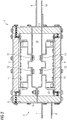
- FIG. 1 shows an embodiment of the power semiconductor module 1 according to the invention in a perspective view.
- the power semiconductor module 1 shown has a module housing 2, which consists of an upper module housing wall 3, a lower module housing wall 4 and Modulmatiwandept 5.
- a module housing 2 which consists of an upper module housing wall 3, a lower module housing wall 4 and Modulmatiwandept 5.
- profile rails 6 are provided, which are firmly bolted to the respective walls.
- front terminals 7 and 8 and rear terminals 9 and 10 are provided.
- the terminals 8 and 10 are at a ground potential, while the terminals 7 and 9 are at a comparatively higher potential, for example 1 kilovolt.
- FIG. 2 shows the power semiconductor module 1 according to FIG. 1 in a cross-sectional side view, in which the upper module housing wall 3, the lower module housing wall 4 and the Modulmatiwandept 5 are better visible.
- the upper module housing wall 3 and the lower module housing wall 4 are each connected to a power semiconductor unit 11.
- Each of the power semiconductor units 11 has in its interior schematically illustrated power semiconductors, which are connected to one another via bonding wires and other interconnects.
- For connecting the power semiconductor units 11 to the terminals 7, 8, 9, 10 are terminals 12.
- the electrical connection of the terminals 12 with the schematically indicated in Figure 2 power semiconductors or power semiconductor chips is in FIG. 2 not shown for reasons of clarity. The connection, not shown, is arbitrary within the scope of the invention.
- the power semiconductor units 11 are constructed identically and are arranged facing each other so that their power semiconductors or power semiconductor chips conduct heat are connected to the upper module housing wall 3 and the lower Modulgephaseusewandung 4.
- the said modulus walls 3, 4 simultaneously serve as cooling plates 3, 4 of the power semiconductors of the power semiconductor units 11.
- the cooling plates 3, 4, which are anyway necessary for the operation of the power semiconductor units 11, simultaneously form the upper or lower boundary wall of the power semiconductor module 1. In this way, a low-cost module housing 2 is provided.
- the compact and cost-effective housing 2 simultaneously forms an explosion protection.
- the power semiconductor units 11 are commercially available power semiconductor units, which in turn generally have their own unit housing in which power semiconductor chips are in turn arranged as power semiconductors.
- the power semiconductor chips of the power semiconductor units 11 are at least partially connected to one another via bonding wires. Due to this connection of the power semiconductor chips of the power semiconductor units 11, melting of the bonding wires may occur, in particular in the case of high short-circuit currents, with arc development in the wake. The arc releases explosive gases, which are due to the facing arrangement of the power semiconductor units 11 substantially directed against the stable opposite cooling plate 3, 4 as the upper and lower housing.
- Each power semiconductor unit 11 is surrounded by a holding ring 13, which is firmly screwed with its flange portion on the respective cooling plate 3, 4.
- the side wall section of the holding ring 13 projecting from the respective cooling plate 3, 4 encloses the respective power semiconductor unit 11 and thus forms an additional explosion protection.
- the retaining ring 13 is made of steel, for example.
- a filling space 14 is provided between the terminals 12 of the power semiconductor units 11, in which a temperature-resistant filler is arranged.
- the filler is for example a non-conductive temperature-resistant plastic. In the event of an explosion, the plastic deforms and absorbs the released explosion energy.
- the Modulfacewandungen 5 are made in the embodiments shown from a non-conductive insulating material, for example, a plastic reinforced with glass fibers, but also metallic, ie electrically conductive materials, for the Modulmatiwandept 5 also come into question.
- the Moduleitenwandept 5 are penetrated by the terminal 7 and the terminals 9 and 10, so that a simple connection of the power semiconductor module 1 is made possible from the outside.
- the power semiconductor module 1 is advantageously parallel with a capacitor or another energy store switched, wherein the parallel circuit of power semiconductor module 1 and energy storage form a branch module.
- a series circuit of branch modules in turn forms a power converter branch, which is part of a multilevel power converter.
- Such multilevel converters are used, for example, in high voltage direct current transmission.
Landscapes
- Engineering & Computer Science (AREA)
- Microelectronics & Electronic Packaging (AREA)
- Power Conversion In General (AREA)
- Cooling Or The Like Of Semiconductors Or Solid State Devices (AREA)
Claims (6)
- Module (1) à semi-conducteur de puissance, comprenant au moins deux unités (11) à semi-conducteur de puissance connectées entre elles, qui ont chacune un boîtier d'unité dans lequel sont disposées des semi-conducteurs de puissance pouvant être mis à l'état passant, dans lequel, à chaque unité (11) à semi-conducteur de puissance est associée une plaque (3, 4) de refroidissement par laquelle les semi-conducteurs de puissance pouvant être mis à l'état passant sont reliés de manière à conduire la chaleur, les semi-conducteurs de puissance étant des puces à semi-conducteur de puissance et comprenant un boîtier de module, dans lequel les unités à semi-conducteur de puissance sont disposées, les plaques (3, 4) de refroidissement formant une face supérieure et une face inférieure du boîtier du module, le boîtier (2) du module disposant de parois (5) latérales, qui s'étendent entre les plaques (3, 4) de refroidissement et qui sont en un matériau isolant,
dans lequel le module à semi-conducteur de puissance dispose de bornes (7, 8, 9, 10) de connexion pour la connexion des unités (11) à semi-conducteur de puissance, le module à semi-conducteur de puissance étant caractérisé en ce que les bornes (7, 8, 9, 10) de connexion passent à travers les parois latérales. - Module (1) à semi-conducteur de puissance suivant la revendication 1,
caractérisé en ce que
les unités (11) à semi-conducteur de puissance sont tournées l'une vers l'autre. - Module (1) à semi-conducteur de puissance suivant l'une des revendications précédentes,
caractérisé en ce que les semi-conducteurs de puissance sont reliés entre eux au moyen de fils de liaison. - Module (1) à semi-conducteur de puissance suivant l'une des revendications précédentes,
caractérisé par
au moins une couronne de maintien, qui est reliée fixement à une plaque (3, 4) de refroidissement et qui a une partie de paroi de plaque, qui fait saillie de la plaque de refroidissement et qui entoure, au moins en partie, une unité (11) à semi-conducteur de puissance. - Branche de soupape de convertisseur,
caractérisée par
un montage série de module (1) à semi-conducteur de puissance suivant l'une des revendications précédentes. - Convertisseur
caractérisé par
un montage en pont de branches de soupape de convertisseur suivant la revendication 5.
Priority Applications (1)
| Application Number | Priority Date | Filing Date | Title |
|---|---|---|---|
| PL07819865T PL2208225T3 (pl) | 2007-11-13 | 2007-11-13 | Moduł półprzewodnikowy mocy |
Applications Claiming Priority (1)
| Application Number | Priority Date | Filing Date | Title |
|---|---|---|---|
| PCT/EP2007/009995 WO2009062534A1 (fr) | 2007-11-13 | 2007-11-13 | Module semi-conducteur de puissance |
Publications (2)
| Publication Number | Publication Date |
|---|---|
| EP2208225A1 EP2208225A1 (fr) | 2010-07-21 |
| EP2208225B1 true EP2208225B1 (fr) | 2018-10-10 |
Family
ID=39619082
Family Applications (1)
| Application Number | Title | Priority Date | Filing Date |
|---|---|---|---|
| EP07819865.2A Active EP2208225B1 (fr) | 2007-11-13 | 2007-11-13 | Module semi-conducteur de puissance |
Country Status (7)
| Country | Link |
|---|---|
| US (1) | US9064737B2 (fr) |
| EP (1) | EP2208225B1 (fr) |
| JP (1) | JP5127929B2 (fr) |
| CN (1) | CN101855723B (fr) |
| ES (1) | ES2705170T3 (fr) |
| PL (1) | PL2208225T3 (fr) |
| WO (1) | WO2009062534A1 (fr) |
Families Citing this family (27)
| Publication number | Priority date | Publication date | Assignee | Title |
|---|---|---|---|---|
| DE502005007115D1 (de) * | 2005-06-23 | 2009-05-28 | Siemens Ag | Elektronikmodul |
| BRPI0924756B1 (pt) * | 2009-03-13 | 2018-10-23 | Fraunhofer-Gesellschaft Zur Foerderung Der Angewandten Forschung E.V. | módulo semicondutor de energia tendo paredes laterais isolantes dispostas em camadas |
| CN101651135B (zh) * | 2009-08-12 | 2010-12-29 | 荣信电力电子股份有限公司 | 66kV光控水冷晶闸管阀组 |
| US9247655B2 (en) | 2010-06-11 | 2016-01-26 | Honeywell International Inc. | Sheet metal explosion-proof, and flame-proof enclosures |
| WO2012088676A1 (fr) * | 2010-12-29 | 2012-07-05 | 荣信电力电子股份有限公司 | Rangée de valves à thyristor refroidies par eau et commandées par une lumière de 66 kv |
| EP2707956A1 (fr) * | 2011-05-10 | 2014-03-19 | ABB Research Ltd. | Module de puissance et son procédé de fonctionnement |
| JP5743811B2 (ja) * | 2011-08-29 | 2015-07-01 | 株式会社東芝 | 電力変換装置 |
| DE102013223430A1 (de) * | 2013-11-18 | 2015-05-21 | BSH Hausgeräte GmbH | Vorrichtung mit einem Leistungselektronikmodul zum Versorgen eines elektrischen Verbrauchers eines Haushaltsgeräts mit elektrischer Versorgungsspannung, Haushaltsgerät und Verfahren zum Herstellen einer derartigen Vorrichtung |
| EP3007220A1 (fr) * | 2014-10-10 | 2016-04-13 | ABB Technology AG | Dispositif de semi-conducteur de puissance comportant éléments de protection contre explosion ou rupture |
| WO2016165843A1 (fr) * | 2015-04-13 | 2016-10-20 | Abb Technology Ag | Module électronique de puissance |
| JP5926835B2 (ja) * | 2015-04-23 | 2016-05-25 | 株式会社東芝 | 電力変換装置 |
| EP3366093B1 (fr) * | 2015-12-22 | 2020-09-16 | Siemens Aktiengesellschaft | Module électrique avec composants électriques |
| DE102016202600A1 (de) | 2016-02-19 | 2017-08-24 | Siemens Aktiengesellschaft | Elektrisches Modul mit elektrischer Komponente |
| DE102016202734A1 (de) * | 2016-02-23 | 2017-08-24 | Siemens Aktiengesellschaft | Elektrische Einrichtung mit elektrischen Modulen |
| WO2017162264A1 (fr) | 2016-03-21 | 2017-09-28 | Siemens Aktiengesellschaft | Dispositif électrique et installation électrique comprenant un système de refroidissement |
| JP6765444B2 (ja) | 2016-12-22 | 2020-10-07 | 三菱電機株式会社 | 電力変換装置 |
| WO2019117119A1 (fr) * | 2017-12-14 | 2019-06-20 | 日本電産株式会社 | Onduleur, onduleur dans un boîtier, moteur électrique ayant un onduleur intégré, et dispositif composite ayant un onduleur intégré |
| FR3076175B1 (fr) * | 2017-12-22 | 2020-01-10 | Valeo Siemens Eautomotive France Sas | Equipement electrique a paroi deportee |
| DE102018204625A1 (de) | 2018-03-27 | 2019-10-02 | Siemens Aktiengesellschaft | Gehäuse für einen Umrichter, Endstufe eines Umrichters mit einem derartigen Gehäuse, Umrichter sowie Luftfahrzeug mit einem Umrichter |
| AT521041B1 (de) * | 2018-05-25 | 2019-10-15 | Miba Energy Holding Gmbh | Leistungsbaugruppe mit Schottwand |
| CN112544127A (zh) * | 2018-05-25 | 2021-03-23 | 米巴能源控股有限公司 | 具有定义的转载路径的功率结构组件和用于制造的方法 |
| EP3799704B1 (fr) | 2018-07-17 | 2023-11-01 | Siemens Energy Global GmbH & Co. KG | Module semiconducteur de puissance |
| DE102019113193A1 (de) * | 2019-05-17 | 2020-11-19 | R. Stahl Schaltgeräte GmbH | Baukastensystem zum Herstellen eines Gehäuses |
| WO2021117213A1 (fr) | 2019-12-13 | 2021-06-17 | 三菱電機株式会社 | Dispositif de conversion de puissance |
| EP3955282A1 (fr) * | 2020-08-11 | 2022-02-16 | Siemens Aktiengesellschaft | Module de puissance pourvu d'au moins une unité de puissance |
| EP4162524A1 (fr) * | 2021-08-27 | 2023-04-12 | Dynex Semiconductor Limited | Dispositif à semi-conducteur doté de structure de protection contre les défaillances |
| JP7834209B2 (ja) * | 2023-01-30 | 2026-03-23 | 三菱電機株式会社 | 半導体装置 |
Citations (1)
| Publication number | Priority date | Publication date | Assignee | Title |
|---|---|---|---|---|
| US20030198022A1 (en) * | 2002-04-22 | 2003-10-23 | Runqing Ye | Power converter package with enhanced thermal management |
Family Cites Families (32)
| Publication number | Priority date | Publication date | Assignee | Title |
|---|---|---|---|---|
| JPS5635443A (en) | 1979-08-31 | 1981-04-08 | Toshiba Corp | Semiconductor device |
| EP0033399B1 (fr) | 1980-02-01 | 1985-04-17 | BBC Aktiengesellschaft Brown, Boveri & Cie. | Dispositif à composant semiconducteur protégé contre des explosions |
| DE3521572A1 (de) * | 1985-06-15 | 1986-12-18 | Brown, Boveri & Cie Ag, 6800 Mannheim | Leistungshalbleitermodul mit keramiksubstrat |
| US4878106A (en) * | 1986-12-02 | 1989-10-31 | Anton Piller Gmbh & Co. Kg | Semiconductor circuit packages for use in high power applications and method of making the same |
| US4963976A (en) * | 1988-09-12 | 1990-10-16 | Sundstrand Corporation | Integrated electrical conducting, cooling and clamping assembly for power semiconductors |
| DE69018846T2 (de) * | 1989-02-10 | 1995-08-24 | Fujitsu Ltd | Keramische Packung vom Halbleiteranordnungstyp und Verfahren zum Zusammensetzen derselben. |
| DE4418426B4 (de) * | 1993-09-08 | 2007-08-02 | Mitsubishi Denki K.K. | Halbleiterleistungsmodul und Verfahren zur Herstellung des Halbleiterleistungsmoduls |
| DE4407810C2 (de) | 1994-03-09 | 1998-02-26 | Semikron Elektronik Gmbh | Schaltungsanordnung (Modul) |
| JP3357220B2 (ja) * | 1995-07-07 | 2002-12-16 | 三菱電機株式会社 | 半導体装置 |
| JPH09140159A (ja) * | 1995-11-10 | 1997-05-27 | Teikoku Denki Seisakusho:Kk | 防爆インバータ盤 |
| JP3879150B2 (ja) | 1996-08-12 | 2007-02-07 | 株式会社デンソー | 半導体装置 |
| DE19649798A1 (de) * | 1996-12-02 | 1998-06-04 | Abb Research Ltd | Leistungshalbleitermodul |
| JPH10335579A (ja) * | 1997-05-27 | 1998-12-18 | Toshiba Corp | 大電力半導体モジュール装置 |
| TW408453B (en) * | 1997-12-08 | 2000-10-11 | Toshiba Kk | Package for semiconductor power device and method for assembling the same |
| JP3864282B2 (ja) * | 1998-09-22 | 2006-12-27 | 三菱マテリアル株式会社 | パワーモジュール用基板及びその製造方法並びにこの基板を用いた半導体装置 |
| WO2000055917A1 (fr) | 1999-03-17 | 2000-09-21 | eupec Europäische Gesellschaft für Leistungshalbleiter mbH & Co. KG | Module a semiconducteur de puissance |
| JP4044265B2 (ja) * | 2000-05-16 | 2008-02-06 | 三菱電機株式会社 | パワーモジュール |
| JP2002026251A (ja) * | 2000-07-11 | 2002-01-25 | Toshiba Corp | 半導体装置 |
| DE10039770A1 (de) | 2000-08-16 | 2002-02-28 | Bosch Gmbh Robert | Kühlvorrichtung |
| JP2002203942A (ja) * | 2000-12-28 | 2002-07-19 | Fuji Electric Co Ltd | パワー半導体モジュール |
| EP1263045A1 (fr) * | 2001-06-01 | 2002-12-04 | ABB Schweiz AG | Module semi-conducteur à haute prestation |
| JP3627738B2 (ja) * | 2001-12-27 | 2005-03-09 | 株式会社デンソー | 半導体装置 |
| RU25250U1 (ru) | 2002-04-01 | 2002-09-20 | Открытое акционерное общество "Всероссийский научно-исследовательский проектно-конструкторский и технологический институт релестроения с опытным производством" | Силовой высоковольтный блок |
| US6989592B2 (en) * | 2002-05-01 | 2006-01-24 | The Boeing Company | Integrated power module with reduced thermal impedance |
| DE102004018477B4 (de) | 2004-04-16 | 2008-08-21 | Infineon Technologies Ag | Halbleitermodul |
| JP2006190972A (ja) * | 2004-12-08 | 2006-07-20 | Mitsubishi Electric Corp | 電力用半導体装置 |
| US7598603B2 (en) * | 2006-03-15 | 2009-10-06 | Infineon Technologies Ag | Electronic component having a power switch with an anode thereof mounted on a die attach region of a heat sink |
| JP4816214B2 (ja) * | 2006-04-13 | 2011-11-16 | 株式会社デンソー | 半導体装置及びその製造方法 |
| CN200956368Y (zh) | 2006-06-16 | 2007-10-03 | 无锡天和电子有限公司 | 半导体功率器件的贴装式封装外壳 |
| JP4878520B2 (ja) | 2006-08-09 | 2012-02-15 | 本田技研工業株式会社 | 半導体装置 |
| US7701054B2 (en) | 2007-02-12 | 2010-04-20 | Infineon Technologies Ag | Power semiconductor module and method for its manufacture |
| BRPI0924756B1 (pt) * | 2009-03-13 | 2018-10-23 | Fraunhofer-Gesellschaft Zur Foerderung Der Angewandten Forschung E.V. | módulo semicondutor de energia tendo paredes laterais isolantes dispostas em camadas |
-
2007
- 2007-11-13 WO PCT/EP2007/009995 patent/WO2009062534A1/fr not_active Ceased
- 2007-11-13 EP EP07819865.2A patent/EP2208225B1/fr active Active
- 2007-11-13 CN CN2007801014993A patent/CN101855723B/zh active Active
- 2007-11-13 ES ES07819865T patent/ES2705170T3/es active Active
- 2007-11-13 PL PL07819865T patent/PL2208225T3/pl unknown
- 2007-11-13 JP JP2010532442A patent/JP5127929B2/ja active Active
- 2007-11-13 US US12/741,737 patent/US9064737B2/en active Active
Patent Citations (1)
| Publication number | Priority date | Publication date | Assignee | Title |
|---|---|---|---|---|
| US20030198022A1 (en) * | 2002-04-22 | 2003-10-23 | Runqing Ye | Power converter package with enhanced thermal management |
Also Published As
| Publication number | Publication date |
|---|---|
| ES2705170T3 (es) | 2019-03-22 |
| US20100265744A1 (en) | 2010-10-21 |
| JP2011503852A (ja) | 2011-01-27 |
| PL2208225T3 (pl) | 2019-03-29 |
| WO2009062534A1 (fr) | 2009-05-22 |
| US9064737B2 (en) | 2015-06-23 |
| CN101855723A (zh) | 2010-10-06 |
| JP5127929B2 (ja) | 2013-01-23 |
| EP2208225A1 (fr) | 2010-07-21 |
| CN101855723B (zh) | 2012-04-25 |
Similar Documents
| Publication | Publication Date | Title |
|---|---|---|
| EP2208225B1 (fr) | Module semi-conducteur de puissance | |
| EP2356894B1 (fr) | Module redresseur de courant avec rails refroidis | |
| EP1318547B1 (fr) | Module semi-conducteur à haut prestation | |
| EP2524431B1 (fr) | Circuit de disjoncteurs électroniques d'un générateur de courant | |
| DE10037379B4 (de) | Modular aufgebauter Stromrichter | |
| DE102011104928B4 (de) | Kühlungsaufbau eines Kondensators und Umrichter damit | |
| EP2407015B1 (fr) | Module à semi-conducteurs de puissance pourvu de parois latérales isolantes à structure en couches | |
| EP2095417B1 (fr) | Structure de modules à l'épreuve des explosions pour des composants de puissance, en particulier des composants semi-conducteurs de puissance et leur production | |
| DE112013003222T5 (de) | Halbleitervorrichtung und Halbleitervorrichtungsverbindungsstruktur | |
| DE102007003875A1 (de) | Stromrichter | |
| DE102014104856A1 (de) | Explosionsgeschütztes Leistungshalbleitermodul | |
| EP2989660B1 (fr) | Empilement de semi-conducteurs pour convertisseur équipé de condensateurs d'amortissement | |
| DE112019006927T5 (de) | Halbleitervorrichtung, herstellungsverfahren für eine halbleitervorrichtung sowie leistungswandler | |
| WO2018210506A1 (fr) | Système de commutation à semi-conducteurs | |
| EP0185181B1 (fr) | Circuit à anode-cathode à inductance réduite d'un thyristor GTO de puissance | |
| EP0994557A2 (fr) | Convertisseur avec condensateur à basse inductance dans le circuit intermédiaire | |
| WO2009127179A1 (fr) | Procédé de fabrication et structure d'un module de puissance | |
| EP2564501B1 (fr) | Sous-module destiné à un convertisseur modulaire à étages multiples | |
| DE4023687A1 (de) | Stromrichteranordnung | |
| WO2008074274A1 (fr) | Construction mécanique d'un convertisseur multi-niveaux modulaire dont les modules convertisseurs sont fixés de façon porteuse aux accumulateurs d'énergie | |
| DE29805943U1 (de) | Niederinduktive Verschienung zweier mehrlagiger Stromschienenanordnungen für Stromrichter | |
| WO2025061430A1 (fr) | Agencement pour dissipateurs thermiques dans un convertisseur multiniveau | |
| DE102021105114A1 (de) | Brückenschaltkreis, Leistungsmodul und damit versehenes Antriebssystem | |
| DE102022133265A1 (de) | Leistungselektronikanordnung für eine elektrische Maschine und Kraftfahrzeug | |
| EP3738134A1 (fr) | Dispositif pour protéger un semi-conducteur de puissance dans une cuve remplie d'un fluide isolant |
Legal Events
| Date | Code | Title | Description |
|---|---|---|---|
| PUAI | Public reference made under article 153(3) epc to a published international application that has entered the european phase |
Free format text: ORIGINAL CODE: 0009012 |
|
| 17P | Request for examination filed |
Effective date: 20100414 |
|
| AK | Designated contracting states |
Kind code of ref document: A1 Designated state(s): AT BE BG CH CY CZ DE DK EE ES FI FR GB GR HU IE IS IT LI LT LU LV MC MT NL PL PT RO SE SI SK TR |
|
| AX | Request for extension of the european patent |
Extension state: AL BA HR MK RS |
|
| DAX | Request for extension of the european patent (deleted) | ||
| RAP1 | Party data changed (applicant data changed or rights of an application transferred) |
Owner name: SIEMENS AKTIENGESELLSCHAFT |
|
| 17Q | First examination report despatched |
Effective date: 20170418 |
|
| RAP1 | Party data changed (applicant data changed or rights of an application transferred) |
Owner name: SIEMENS AKTIENGESELLSCHAFT |
|
| GRAP | Despatch of communication of intention to grant a patent |
Free format text: ORIGINAL CODE: EPIDOSNIGR1 |
|
| RIC1 | Information provided on ipc code assigned before grant |
Ipc: H01L 25/11 20060101ALI20180416BHEP Ipc: H01L 25/07 20060101ALN20180416BHEP Ipc: H01L 23/40 20060101AFI20180416BHEP Ipc: H05K 7/14 20060101ALI20180416BHEP |
|
| INTG | Intention to grant announced |
Effective date: 20180507 |
|
| GRAS | Grant fee paid |
Free format text: ORIGINAL CODE: EPIDOSNIGR3 |
|
| GRAA | (expected) grant |
Free format text: ORIGINAL CODE: 0009210 |
|
| AK | Designated contracting states |
Kind code of ref document: B1 Designated state(s): AT BE BG CH CY CZ DE DK EE ES FI FR GB GR HU IE IS IT LI LT LU LV MC MT NL PL PT RO SE SI SK TR |
|
| REG | Reference to a national code |
Ref country code: GB Ref legal event code: FG4D Free format text: NOT ENGLISH |
|
| REG | Reference to a national code |
Ref country code: CH Ref legal event code: EP Ref country code: AT Ref legal event code: REF Ref document number: 1052231 Country of ref document: AT Kind code of ref document: T Effective date: 20181015 |
|
| REG | Reference to a national code |
Ref country code: IE Ref legal event code: FG4D Free format text: LANGUAGE OF EP DOCUMENT: GERMAN |
|
| REG | Reference to a national code |
Ref country code: DE Ref legal event code: R096 Ref document number: 502007016432 Country of ref document: DE |
|
| REG | Reference to a national code |
Ref country code: SE Ref legal event code: TRGR |
|
| REG | Reference to a national code |
Ref country code: NL Ref legal event code: MP Effective date: 20181010 |
|
| REG | Reference to a national code |
Ref country code: LT Ref legal event code: MG4D |
|
| REG | Reference to a national code |
Ref country code: ES Ref legal event code: FG2A Ref document number: 2705170 Country of ref document: ES Kind code of ref document: T3 Effective date: 20190322 |
|
| PG25 | Lapsed in a contracting state [announced via postgrant information from national office to epo] |
Ref country code: NL Free format text: LAPSE BECAUSE OF FAILURE TO SUBMIT A TRANSLATION OF THE DESCRIPTION OR TO PAY THE FEE WITHIN THE PRESCRIBED TIME-LIMIT Effective date: 20181010 |
|
| PG25 | Lapsed in a contracting state [announced via postgrant information from national office to epo] |
Ref country code: BG Free format text: LAPSE BECAUSE OF FAILURE TO SUBMIT A TRANSLATION OF THE DESCRIPTION OR TO PAY THE FEE WITHIN THE PRESCRIBED TIME-LIMIT Effective date: 20190110 Ref country code: LT Free format text: LAPSE BECAUSE OF FAILURE TO SUBMIT A TRANSLATION OF THE DESCRIPTION OR TO PAY THE FEE WITHIN THE PRESCRIBED TIME-LIMIT Effective date: 20181010 Ref country code: FI Free format text: LAPSE BECAUSE OF FAILURE TO SUBMIT A TRANSLATION OF THE DESCRIPTION OR TO PAY THE FEE WITHIN THE PRESCRIBED TIME-LIMIT Effective date: 20181010 Ref country code: IS Free format text: LAPSE BECAUSE OF FAILURE TO SUBMIT A TRANSLATION OF THE DESCRIPTION OR TO PAY THE FEE WITHIN THE PRESCRIBED TIME-LIMIT Effective date: 20190210 Ref country code: LV Free format text: LAPSE BECAUSE OF FAILURE TO SUBMIT A TRANSLATION OF THE DESCRIPTION OR TO PAY THE FEE WITHIN THE PRESCRIBED TIME-LIMIT Effective date: 20181010 |
|
| PG25 | Lapsed in a contracting state [announced via postgrant information from national office to epo] |
Ref country code: PT Free format text: LAPSE BECAUSE OF FAILURE TO SUBMIT A TRANSLATION OF THE DESCRIPTION OR TO PAY THE FEE WITHIN THE PRESCRIBED TIME-LIMIT Effective date: 20190210 Ref country code: GR Free format text: LAPSE BECAUSE OF FAILURE TO SUBMIT A TRANSLATION OF THE DESCRIPTION OR TO PAY THE FEE WITHIN THE PRESCRIBED TIME-LIMIT Effective date: 20190111 |
|
| REG | Reference to a national code |
Ref country code: CH Ref legal event code: PL |
|
| REG | Reference to a national code |
Ref country code: DE Ref legal event code: R097 Ref document number: 502007016432 Country of ref document: DE |
|
| PG25 | Lapsed in a contracting state [announced via postgrant information from national office to epo] |
Ref country code: LU Free format text: LAPSE BECAUSE OF NON-PAYMENT OF DUE FEES Effective date: 20181113 Ref country code: CZ Free format text: LAPSE BECAUSE OF FAILURE TO SUBMIT A TRANSLATION OF THE DESCRIPTION OR TO PAY THE FEE WITHIN THE PRESCRIBED TIME-LIMIT Effective date: 20181010 Ref country code: DK Free format text: LAPSE BECAUSE OF FAILURE TO SUBMIT A TRANSLATION OF THE DESCRIPTION OR TO PAY THE FEE WITHIN THE PRESCRIBED TIME-LIMIT Effective date: 20181010 |
|
| PLBE | No opposition filed within time limit |
Free format text: ORIGINAL CODE: 0009261 |
|
| STAA | Information on the status of an ep patent application or granted ep patent |
Free format text: STATUS: NO OPPOSITION FILED WITHIN TIME LIMIT |
|
| REG | Reference to a national code |
Ref country code: IE Ref legal event code: MM4A |
|
| PG25 | Lapsed in a contracting state [announced via postgrant information from national office to epo] |
Ref country code: MC Free format text: LAPSE BECAUSE OF FAILURE TO SUBMIT A TRANSLATION OF THE DESCRIPTION OR TO PAY THE FEE WITHIN THE PRESCRIBED TIME-LIMIT Effective date: 20181010 Ref country code: CH Free format text: LAPSE BECAUSE OF NON-PAYMENT OF DUE FEES Effective date: 20181130 Ref country code: RO Free format text: LAPSE BECAUSE OF FAILURE TO SUBMIT A TRANSLATION OF THE DESCRIPTION OR TO PAY THE FEE WITHIN THE PRESCRIBED TIME-LIMIT Effective date: 20181010 Ref country code: EE Free format text: LAPSE BECAUSE OF FAILURE TO SUBMIT A TRANSLATION OF THE DESCRIPTION OR TO PAY THE FEE WITHIN THE PRESCRIBED TIME-LIMIT Effective date: 20181010 Ref country code: LI Free format text: LAPSE BECAUSE OF NON-PAYMENT OF DUE FEES Effective date: 20181130 Ref country code: SK Free format text: LAPSE BECAUSE OF FAILURE TO SUBMIT A TRANSLATION OF THE DESCRIPTION OR TO PAY THE FEE WITHIN THE PRESCRIBED TIME-LIMIT Effective date: 20181010 |
|
| 26N | No opposition filed |
Effective date: 20190711 |
|
| PG25 | Lapsed in a contracting state [announced via postgrant information from national office to epo] |
Ref country code: IE Free format text: LAPSE BECAUSE OF NON-PAYMENT OF DUE FEES Effective date: 20181113 Ref country code: SI Free format text: LAPSE BECAUSE OF FAILURE TO SUBMIT A TRANSLATION OF THE DESCRIPTION OR TO PAY THE FEE WITHIN THE PRESCRIBED TIME-LIMIT Effective date: 20181010 |
|
| REG | Reference to a national code |
Ref country code: AT Ref legal event code: MM01 Ref document number: 1052231 Country of ref document: AT Kind code of ref document: T Effective date: 20181113 |
|
| PG25 | Lapsed in a contracting state [announced via postgrant information from national office to epo] |
Ref country code: AT Free format text: LAPSE BECAUSE OF NON-PAYMENT OF DUE FEES Effective date: 20181113 Ref country code: MT Free format text: LAPSE BECAUSE OF FAILURE TO SUBMIT A TRANSLATION OF THE DESCRIPTION OR TO PAY THE FEE WITHIN THE PRESCRIBED TIME-LIMIT Effective date: 20181010 |
|
| PG25 | Lapsed in a contracting state [announced via postgrant information from national office to epo] |
Ref country code: TR Free format text: LAPSE BECAUSE OF FAILURE TO SUBMIT A TRANSLATION OF THE DESCRIPTION OR TO PAY THE FEE WITHIN THE PRESCRIBED TIME-LIMIT Effective date: 20181010 |
|
| PG25 | Lapsed in a contracting state [announced via postgrant information from national office to epo] |
Ref country code: HU Free format text: LAPSE BECAUSE OF FAILURE TO SUBMIT A TRANSLATION OF THE DESCRIPTION OR TO PAY THE FEE WITHIN THE PRESCRIBED TIME-LIMIT; INVALID AB INITIO Effective date: 20071113 Ref country code: CY Free format text: LAPSE BECAUSE OF FAILURE TO SUBMIT A TRANSLATION OF THE DESCRIPTION OR TO PAY THE FEE WITHIN THE PRESCRIBED TIME-LIMIT Effective date: 20181010 |
|
| REG | Reference to a national code |
Ref country code: DE Ref legal event code: R081 Ref document number: 502007016432 Country of ref document: DE Owner name: SIEMENS ENERGY GLOBAL GMBH & CO. KG, DE Free format text: FORMER OWNER: SIEMENS AKTIENGESELLSCHAFT, 80333 MUENCHEN, DE |
|
| REG | Reference to a national code |
Ref country code: GB Ref legal event code: 732E Free format text: REGISTERED BETWEEN 20220908 AND 20220914 |
|
| REG | Reference to a national code |
Ref country code: BE Ref legal event code: PD Owner name: SIEMENS ENERGY GLOBAL GMBH & CO. KG; DE Free format text: DETAILS ASSIGNMENT: CHANGE OF OWNER(S), ASSIGNMENT; FORMER OWNER NAME: SIEMENS AKTIENGESELLSCHAFT Effective date: 20221214 |
|
| P01 | Opt-out of the competence of the unified patent court (upc) registered |
Effective date: 20231222 |
|
| REG | Reference to a national code |
Ref country code: ES Ref legal event code: PC2A Owner name: SIEMENS ENERGY GLOBAL GMBH & CO. KG Effective date: 20240409 |
|
| REG | Reference to a national code |
Ref country code: DE Ref legal event code: R079 Ref document number: 502007016432 Country of ref document: DE Free format text: PREVIOUS MAIN CLASS: H01L0023400000 Ipc: H10W0040600000 |
|
| PGFP | Annual fee paid to national office [announced via postgrant information from national office to epo] |
Ref country code: DE Payment date: 20251126 Year of fee payment: 19 |
|
| PGFP | Annual fee paid to national office [announced via postgrant information from national office to epo] |
Ref country code: GB Payment date: 20251125 Year of fee payment: 19 |
|
| PGFP | Annual fee paid to national office [announced via postgrant information from national office to epo] |
Ref country code: IT Payment date: 20251121 Year of fee payment: 19 |
|
| PGFP | Annual fee paid to national office [announced via postgrant information from national office to epo] |
Ref country code: FR Payment date: 20251124 Year of fee payment: 19 |
|
| PGFP | Annual fee paid to national office [announced via postgrant information from national office to epo] |
Ref country code: BE Payment date: 20251124 Year of fee payment: 19 |
|
| PGFP | Annual fee paid to national office [announced via postgrant information from national office to epo] |
Ref country code: SE Payment date: 20251124 Year of fee payment: 19 |
|
| PGFP | Annual fee paid to national office [announced via postgrant information from national office to epo] |
Ref country code: PL Payment date: 20251020 Year of fee payment: 19 |
|
| PGFP | Annual fee paid to national office [announced via postgrant information from national office to epo] |
Ref country code: ES Payment date: 20251209 Year of fee payment: 19 |