EP2208237B2 - Dispositif de positionnement pour positionner une ou plusieurs cartes de circuit électronique, en particulier pour des piles photovoltaïques, dans une unité de dépôt de métal - Google Patents
Dispositif de positionnement pour positionner une ou plusieurs cartes de circuit électronique, en particulier pour des piles photovoltaïques, dans une unité de dépôt de métal Download PDFInfo
- Publication number
- EP2208237B2 EP2208237B2 EP07847831.0A EP07847831A EP2208237B2 EP 2208237 B2 EP2208237 B2 EP 2208237B2 EP 07847831 A EP07847831 A EP 07847831A EP 2208237 B2 EP2208237 B2 EP 2208237B2
- Authority
- EP
- European Patent Office
- Prior art keywords
- positioning device
- strip
- electronic circuit
- frame
- circuit boards
- Prior art date
- Legal status (The legal status is an assumption and is not a legal conclusion. Google has not performed a legal analysis and makes no representation as to the accuracy of the status listed.)
- Not-in-force
Links
Images


Classifications
-
- H—ELECTRICITY
- H10—SEMICONDUCTOR DEVICES; ELECTRIC SOLID-STATE DEVICES NOT OTHERWISE PROVIDED FOR
- H10F—INORGANIC SEMICONDUCTOR DEVICES SENSITIVE TO INFRARED RADIATION, LIGHT, ELECTROMAGNETIC RADIATION OF SHORTER WAVELENGTH OR CORPUSCULAR RADIATION
- H10F71/00—Manufacture or treatment of devices covered by this subclass
-
- H—ELECTRICITY
- H10—SEMICONDUCTOR DEVICES; ELECTRIC SOLID-STATE DEVICES NOT OTHERWISE PROVIDED FOR
- H10P—GENERIC PROCESSES OR APPARATUS FOR THE MANUFACTURE OR TREATMENT OF DEVICES COVERED BY CLASS H10
- H10P72/00—Handling or holding of wafers, substrates or devices during manufacture or treatment thereof
- H10P72/70—Handling or holding of wafers, substrates or devices during manufacture or treatment thereof for supporting or gripping
- H10P72/76—Handling or holding of wafers, substrates or devices during manufacture or treatment thereof for supporting or gripping using mechanical means, e.g. clamps or pinches
- H10P72/7604—Handling or holding of wafers, substrates or devices during manufacture or treatment thereof for supporting or gripping using mechanical means, e.g. clamps or pinches the wafers being placed on a susceptor, stage or support
- H10P72/7624—Handling or holding of wafers, substrates or devices during manufacture or treatment thereof for supporting or gripping using mechanical means, e.g. clamps or pinches the wafers being placed on a susceptor, stage or support characterised by the mechanical construction of the susceptor, stage or support
-
- B—PERFORMING OPERATIONS; TRANSPORTING
- B41—PRINTING; LINING MACHINES; TYPEWRITERS; STAMPS
- B41F—PRINTING MACHINES OR PRESSES
- B41F15/00—Screen printers
- B41F15/08—Machines
- B41F15/0863—Machines with a plurality of flat screens mounted on a turntable
-
- B—PERFORMING OPERATIONS; TRANSPORTING
- B41—PRINTING; LINING MACHINES; TYPEWRITERS; STAMPS
- B41F—PRINTING MACHINES OR PRESSES
- B41F15/00—Screen printers
- B41F15/14—Details
- B41F15/16—Printing tables
-
- H—ELECTRICITY
- H10—SEMICONDUCTOR DEVICES; ELECTRIC SOLID-STATE DEVICES NOT OTHERWISE PROVIDED FOR
- H10F—INORGANIC SEMICONDUCTOR DEVICES SENSITIVE TO INFRARED RADIATION, LIGHT, ELECTROMAGNETIC RADIATION OF SHORTER WAVELENGTH OR CORPUSCULAR RADIATION
- H10F71/00—Manufacture or treatment of devices covered by this subclass
- H10F71/137—Batch treatment of the devices
- H10F71/1375—Apparatus for automatic interconnection of photovoltaic cells in a module
-
- H—ELECTRICITY
- H10—SEMICONDUCTOR DEVICES; ELECTRIC SOLID-STATE DEVICES NOT OTHERWISE PROVIDED FOR
- H10F—INORGANIC SEMICONDUCTOR DEVICES SENSITIVE TO INFRARED RADIATION, LIGHT, ELECTROMAGNETIC RADIATION OF SHORTER WAVELENGTH OR CORPUSCULAR RADIATION
- H10F77/00—Constructional details of devices covered by this subclass
- H10F77/20—Electrodes
- H10F77/206—Electrodes for devices having potential barriers
- H10F77/211—Electrodes for devices having potential barriers for photovoltaic cells
-
- H—ELECTRICITY
- H10—SEMICONDUCTOR DEVICES; ELECTRIC SOLID-STATE DEVICES NOT OTHERWISE PROVIDED FOR
- H10P—GENERIC PROCESSES OR APPARATUS FOR THE MANUFACTURE OR TREATMENT OF DEVICES COVERED BY CLASS H10
- H10P72/00—Handling or holding of wafers, substrates or devices during manufacture or treatment thereof
- H10P72/30—Handling or holding of wafers, substrates or devices during manufacture or treatment thereof for conveying, e.g. between different workstations
- H10P72/33—Handling or holding of wafers, substrates or devices during manufacture or treatment thereof for conveying, e.g. between different workstations into and out of processing chamber
- H10P72/3306—Horizontal transfer of a single workpiece
-
- H—ELECTRICITY
- H10—SEMICONDUCTOR DEVICES; ELECTRIC SOLID-STATE DEVICES NOT OTHERWISE PROVIDED FOR
- H10P—GENERIC PROCESSES OR APPARATUS FOR THE MANUFACTURE OR TREATMENT OF DEVICES COVERED BY CLASS H10
- H10P72/00—Handling or holding of wafers, substrates or devices during manufacture or treatment thereof
- H10P72/70—Handling or holding of wafers, substrates or devices during manufacture or treatment thereof for supporting or gripping
- H10P72/76—Handling or holding of wafers, substrates or devices during manufacture or treatment thereof for supporting or gripping using mechanical means, e.g. clamps or pinches
- H10P72/7604—Handling or holding of wafers, substrates or devices during manufacture or treatment thereof for supporting or gripping using mechanical means, e.g. clamps or pinches the wafers being placed on a susceptor, stage or support
- H10P72/7618—Handling or holding of wafers, substrates or devices during manufacture or treatment thereof for supporting or gripping using mechanical means, e.g. clamps or pinches the wafers being placed on a susceptor, stage or support characterised by a movable susceptor, stage or support, others than those only rotating on their own vertical axis, e.g. susceptors on a rotating carrousel
-
- H—ELECTRICITY
- H10—SEMICONDUCTOR DEVICES; ELECTRIC SOLID-STATE DEVICES NOT OTHERWISE PROVIDED FOR
- H10P—GENERIC PROCESSES OR APPARATUS FOR THE MANUFACTURE OR TREATMENT OF DEVICES COVERED BY CLASS H10
- H10P72/00—Handling or holding of wafers, substrates or devices during manufacture or treatment thereof
- H10P72/70—Handling or holding of wafers, substrates or devices during manufacture or treatment thereof for supporting or gripping
- H10P72/76—Handling or holding of wafers, substrates or devices during manufacture or treatment thereof for supporting or gripping using mechanical means, e.g. clamps or pinches
- H10P72/7604—Handling or holding of wafers, substrates or devices during manufacture or treatment thereof for supporting or gripping using mechanical means, e.g. clamps or pinches the wafers being placed on a susceptor, stage or support
- H10P72/7621—Handling or holding of wafers, substrates or devices during manufacture or treatment thereof for supporting or gripping using mechanical means, e.g. clamps or pinches the wafers being placed on a susceptor, stage or support characterised by supporting two or more semiconductor substrates
-
- Y—GENERAL TAGGING OF NEW TECHNOLOGICAL DEVELOPMENTS; GENERAL TAGGING OF CROSS-SECTIONAL TECHNOLOGIES SPANNING OVER SEVERAL SECTIONS OF THE IPC; TECHNICAL SUBJECTS COVERED BY FORMER USPC CROSS-REFERENCE ART COLLECTIONS [XRACs] AND DIGESTS
- Y02—TECHNOLOGIES OR APPLICATIONS FOR MITIGATION OR ADAPTATION AGAINST CLIMATE CHANGE
- Y02E—REDUCTION OF GREENHOUSE GAS [GHG] EMISSIONS, RELATED TO ENERGY GENERATION, TRANSMISSION OR DISTRIBUTION
- Y02E10/00—Energy generation through renewable energy sources
- Y02E10/50—Photovoltaic [PV] energy
-
- Y—GENERAL TAGGING OF NEW TECHNOLOGICAL DEVELOPMENTS; GENERAL TAGGING OF CROSS-SECTIONAL TECHNOLOGIES SPANNING OVER SEVERAL SECTIONS OF THE IPC; TECHNICAL SUBJECTS COVERED BY FORMER USPC CROSS-REFERENCE ART COLLECTIONS [XRACs] AND DIGESTS
- Y02—TECHNOLOGIES OR APPLICATIONS FOR MITIGATION OR ADAPTATION AGAINST CLIMATE CHANGE
- Y02P—CLIMATE CHANGE MITIGATION TECHNOLOGIES IN THE PRODUCTION OR PROCESSING OF GOODS
- Y02P70/00—Climate change mitigation technologies in the production process for final industrial or consumer products
- Y02P70/50—Manufacturing or production processes characterised by the final manufactured product
Definitions
- the present invention concerns a positioning device for electronic circuit boards, in particular but not only green-tape or wafers for photovoltaic cells, in a metal-deposition unit, for example by means of serigraphy.
- the positioning device according to the present invention is applied to a transport member, for example with a rotary turret or a turntable, which transports the electronic circuit boards from a loading station to a discharge station, passing through at least a metal-deposition station.
- Plants for working electronic circuit boards for example those called wafers, are known, for example for the production of photovoltaic cells, which comprise at least a unit to deposit metal tracks on the wafers and a positioning device that positions and transports the wafers with respect to the deposition unit, and possible other working stations.
- a positioning device which comprises at least a belt to feed metal wafers and a rotary turret or turntable, on which the wafers fed by the feed belt are positioned.
- the turret can be rotated by determinate angles in order to transport and position each wafer in defined operating positions of the deposition unit, so as to achieve the photovoltaic cells.
- This type of transport member needs specific members to position the wafers, which comprise at least a supporting plate mounted on the turret and on which the wafer is initially deposited as it exits from the conveyor belt.
- a positioning device is also known in which, instead of the supporting plate, there is a sliding strip on the turret, made of transpirable material, for example paper, wound between two winding/unwinding rollers.
- a sliding strip on the turret made of transpirable material, for example paper, wound between two winding/unwinding rollers.
- One purpose of the present invention is to achieve a positioning device for electronic circuit boards, which is easy and economical to make and which allows to position the boards precisely on the transport member, without long and costly steps being necessary to correct the position of the boards.
- Another purpose of the present invention is to achieve a positioning device for electronic circuit boards which does not need long, complex and costly maintenance steps in order to be replaced.
- the Applicant has devised, tested and embodied the present invention to overcome the shortcomings of the state of the art and to obtain these and other purposes and advantages.
- a positioning device is applied to position electronic circuit boards, for example, but not only, silicon-based wafers, with respect to an operating unit.
- the positioning device comprises a rotary member able to rotate selectively at least between a first operating position and a second operating position, and a positioning member able to be mounted on the rotary member.
- the positioning member comprises at least a frame, which is mounted removably on the rotary member, and a strip made of transpirable material on which each electronic circuit board is rested.
- the strip is wound between a pair of winding/unwinding rollers, pivoted on the frame.
- the positioning device is selectively removable from the rotary element, so that it can be replaced by another, for example of different size and/or function, or simply when the transpirable strip is finished.
- the selective removability of the device thus allows to speed up and simplify the operations to replace the strip, limiting any possible interruptions in production to a minimum, increasing productivity and reducing the overall costs of management of the transport member.
- the removable frame comprises rapid attachment means conformed so as to allow at least the reciprocal mechanical, electric and possibly pneumatic connections of the device to the rotary element, with a limited number of operations, advantageously only the sliding insertion of the frame into a coordinated seating made on the rotary element.
- the device according to the invention comprises at least a driven roller able to be selectively brought into cooperation with one of the two winding/unwinding rollers, so as to determine the movement of the transpirable strip, and hence of the electronic circuit board towards or from the rotary element.
- the driven roller is mounted on the rotary element in correspondence with a loading and/or unloading station for the electronic circuit boards.
- the removable frame also comprises lighting means disposed under the transpirable strip in order to determine a rear-illumination effect, and facilitate operations to control and correct the position of the electronic circuit board on the transpirable strip.
- the removable frame comprises suction means disposed in cooperation with the transpirable strip and able to hold the electronic circuit board, through pneumatic depression, in a determinate operating position above the transpirable strip.
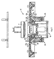
- a positioning device 10 is mounted on a metal-deposition unit 11 of a plant for making photovoltaic cells 12b starting from electronic circuit boards, for example wafers 12a.
- the wafers 12a and the photovoltaic cells 12b are moved and positioned with respect to the metal-deposition unit 11 by means of: a first conveyor belt 13 to feed the wafers 12a; a second conveyor belt 15 to discharge the photovoltaic cells 12b; and a rotary turret 16 interposed between the two belts 13 and 15 which, as will be explained hereafter, transports the wafers 12a and the photovoltaic cells 12b in turntable fashion, between the various operating positions.
- the positioning device 10 comprises one or more positioning members 17, in this case four, offset angularly with respect to each other by 90°, and mounted on the rotary turret 16, inside coordinated assembly seatings 18 made peripherally on the rotary turret 16.
- Each positioning member 17 comprises a removable frame 24 ( fig. 3 ) that comprises rapid attachment members, respectively mechanical 19, electric, 20 and pneumatic 21.
- the mechanical attachment members 19 comprise two linear ribs 22 made along the sides of the frame 24 and able to slide in mating attachment grooves, not shown, made inside each assembly seating 18.
- the linear ribs 22 have an interruption 23 that defines the positioning seating of relative attachment pins 25, in order to temporarily clamp the frame 24 in the relative assembly seating 18.
- the electric attachment members 20 comprise two or more metal platelets 26 mounted on the front wall of the frame 24, and able to be contacted by corresponding conductors, not shown, provided inside the assembly seating 18.
- the pneumatic attachment members 21 comprise two or more pipes 27 also made on the front wall of the frame 24, and able to be connected with corresponding pneumatic connections, not shown, provided inside the assembly seating 18.
- the frame 24 also comprises an upper surface 29 to support the wafer 12a or the photovoltaic cell 12b, and two supporting rollers 30 and 31 around which a paper strip 32 is wound.
- the wafer 12a arriving from the first conveyor belt 13, or the photovoltaic cell 12b to be taken towards the second conveyor belt 15, are positioned on the paper strip 32.
- the upper surface 29 comprises a plurality of suction holes 34, able to define a pneumatic depression which allows the wafer 12a or the photovoltaic cell 12b to be partly held on the frame 24.
- the upper surface 29 is also rear-illuminated so as to promote the possible operations to sight and correct the position of the photovoltaic cell 12b on the paper strip 32.
- the paper strip 32 is disposed initially in a coil on a first of the two supporting rollers 30, it is disposed above the upper surface 29 and is wound onto a second of the two supporting rollers 31.
- the positioning device 10 also comprises ( fig. 2 ) at least a movement mechanism 35, in this case two, mounted on a fixed part of the rotary turret 16, in correspondence with the first conveyor belt 13 and the second conveyor belt 15.
- Each movement mechanism 35 is provided with at least a driven wheel 36 disposed in such a manner as to contact the movement roller 33 and actuate the rotation thereof, to wind the paper strip 32.
- This type of motion transmission is known as a "pinch roller”.
- the device 10 functions as follows.
- figs. 4a to 4e show schematically the movement cycle of a single silicon wafer 12a from which the photovoltaic cell 12b is made. It is clear that in real operating conditions the wafers 12a may be loaded substantially in a continuous cycle, in order to optimize the productivity of the photovoltaic cells 12b.
- the silicon wafers 12a are transported by the first conveyor belt 13 towards the rotary turret 16, which is positioned angularly so as to have a first frame 24 of the positioning device 10 facing towards the first conveyor belt 13, with the paper strip 32 in a winding movement around the second supporting roller 31.
- the silicon wafer 12a is then positioned on the paper strip 32, and is moved by the latter until it reaches a substantially central position with respect to the upper surface 29. Simultaneously with the movement of the silicon wafer 12a, a pneumatic depression is created through the suction holes 34, in order to hold the wafer 12a in close proximity to the paper strip 32, preventing as much as possible any lateral movements thereof.
- the rotary turret 16 is made to rotate by about 90°, to take the silicon wafer 12a into cooperation with the metal-deposition unit 11.
- a new silicon wafer 12a can be loaded, on a paper strip 32 of a following frame 24.
- the rotary turret 16 is rotated by another 90°, so as to take the frame 24 in correspondence with the second conveyor belt 15.
- the paper strip 32 is moved to transport the photovoltaic cell 12b onto the second conveyor belt 15, and thus to discharge it towards other operating stations of the plant.
- the attachment pins 25 are removed, and the corresponding frame 24 is removed from its assembly seating 18 by sliding the mechanical attachment members 19.
- the electric attachment members 20 and the pneumatic attachment members 21 are conformed so as to be automatically disconnected as soon as the frame 24 begins to be removed.
- a new frame 24 is then prepared, or the same frame 24 with a new paper strip 32, and is re-inserted into the assembly seating 18. This is done by sliding the mechanical attachment members 19.
- the electric attachment members 20 and the pneumatic attachment members 21 are conformed so as to be automatically connected as soon as the insertion of the frame 24 into the assembly seating 18 has been completed.
- the mechanical clamping of the frame 24 in the relative assembly seating 18 can be achieved by means of snap-in mechanisms, servo commanded electronically or pneumatically, by same-shape coupling or in other ways, able to guarantee that the frame is clamped in an easily removable manner.
Landscapes
- Engineering & Computer Science (AREA)
- Mechanical Engineering (AREA)
- Container, Conveyance, Adherence, Positioning, Of Wafer (AREA)
- Photovoltaic Devices (AREA)
- Control Of Position Or Direction (AREA)
- Chemical Vapour Deposition (AREA)
- Physical Vapour Deposition (AREA)
Claims (10)
- Dispositif de positionnement pour positionner des cartes de circuit électronique (12a) par rapport à une unité fonctionnelle (11) comprenant un élément rotatif (16) configuré pour tourner sélectivement au moins entre une première position fonctionnelle et une deuxième position fonctionnelle, et un élément de positionnement (17) configuré pour être monté sur ledit élément rotatif (16), caractérisé en ce que ledit élément de positionnement (17) comprend au moins un bâti (24) profilé pour être monté de manière amovible sur ledit élément rotatif (16) et ayant des moyens de fixation rapide (19, 20, 21) qui sont configurés pour permettre au moins les connexions mécaniques et électriques mutuelles du bâti amovible (24) avec ledit élément rotatif (16), et une bande (32) constituée de matériau transpirant, sur laquelle chacune desdites cartes de circuit électronique (12a) est configurée pour être posée, dans lequel la bande (32) est enroulée entre une paire de rouleaux d'enroulement/déroulement (30, 31) commandés en rotation sur ledit bâti (24).
- Dispositif de positionnement selon la revendication 1, caractérisé en ce que lesdits moyens de fixation rapide comprennent une fixation mécanique (19) comprenant des nervures linéaires (22) réalisées le long des côtés dudit bâti amovible (24) et configurées pour coopérer avec des rainures de fixation conjuguées réalisées à l'intérieur de chaque siège d'assemblage (18).
- Dispositif de positionnement selon la revendication 2, caractérisé en ce que lesdites nervures linéaires (22) ont au moins une interruption (23) configurée pour définir le siège de positionnement de goupilles de fixation correspondantes (25), pour le blocage provisoire du bâti amovible (24) dans ledit siège d'assemblage (18).
- Dispositif de positionnement selon l'une quelconque des revendications 1 à 3, caractérisé en ce que les moyens de fixation rapide comprennent une fixation électrique (20) comprenant une ou plusieurs plaques métalliques (26) montées sur une paroi avant dudit bâti amovible (24) et configurées pour venir en contact par des conducteurs électriques correspondants disposés à l'intérieur dudit siège d'assemblage (18).
- Dispositif de positionnement selon l'une quelconque des revendications 1 à 4, caractérisé en ce que les moyens de fixation rapide comprennent une fixation pneumatique (21) comprenant un ou plusieurs tubes (27) réalisés sur une paroi avant dudit bâti amovible (24) et configurés pour se connecter avec des connexions pneumatiques correspondantes disposées à l'intérieur dudit siège d'assemblage (18).
- Dispositif de positionnement selon l'une quelconque des revendications 1 à 5, caractérisé en ce qu'il comprend des moyens de mouvement (35) montés dans des positions fixes déterminées sur ledit élément rotatif (16), de manière à activer le mouvement sélectif de ladite bande transpirante (32) autour de ladite paire de rouleaux d'enroulement/déroulement (30, 31).
- Dispositif de positionnement selon la revendication 6, caractérisé en ce que lesdits moyens de mouvement (35) comprennent au moins un rouleau commandé (36) configuré pour être amené sélectivement en coopération avec un desdits deux rouleaux d'enroulement/déroulement (30, 31), de manière à déterminer le mouvement de ladite bande transpirante (32).
- Dispositif de positionnement selon l'une quelconque des revendications précédentes, caractérisé en ce que le bâti amovible (24) comprend des moyens d'éclairage disposés sous la bande transpirante (32), de manière à déterminer un effet de rétro-éclairage.
- Dispositif de positionnement selon l'une quelconque des revendications précédentes, caractérisé en ce que le bâti amovible (24) comprend des moyens d'aspiration (34) disposés en coopération avec ladite bande transpirante (32) et configurés pour maintenir lesdites cartes de circuit électronique (12a) dans une position fonctionnelle déterminée.
- Dispositif de positionnement selon la revendication 1, dans lequel lesdites cartes de circuit électronique sont des plaquettes à base de silicium.
Applications Claiming Priority (2)
| Application Number | Priority Date | Filing Date | Title |
|---|---|---|---|
| IT000156A ITUD20070156A1 (it) | 2007-09-04 | 2007-09-04 | Disositivo di posizionamento per posizionare uno o piu' wafer a base di silicio, in particolare per celle fotovoltaiche, in un'unita' di deposizione del metallo |
| PCT/EP2007/063336 WO2009030284A1 (fr) | 2007-09-04 | 2007-12-05 | Dispositif de positionnement pour positionner une ou plusieurs cartes de circuit électronique, en particulier pour des piles photovoltaïques, dans une unité de dépôt de métal |
Publications (3)
| Publication Number | Publication Date |
|---|---|
| EP2208237A1 EP2208237A1 (fr) | 2010-07-21 |
| EP2208237B1 EP2208237B1 (fr) | 2011-06-22 |
| EP2208237B2 true EP2208237B2 (fr) | 2014-04-16 |
Family
ID=39535389
Family Applications (1)
| Application Number | Title | Priority Date | Filing Date |
|---|---|---|---|
| EP07847831.0A Not-in-force EP2208237B2 (fr) | 2007-09-04 | 2007-12-05 | Dispositif de positionnement pour positionner une ou plusieurs cartes de circuit électronique, en particulier pour des piles photovoltaïques, dans une unité de dépôt de métal |
Country Status (11)
| Country | Link |
|---|---|
| US (1) | US20100254787A1 (fr) |
| EP (1) | EP2208237B2 (fr) |
| JP (1) | JP5090533B2 (fr) |
| KR (1) | KR20100075879A (fr) |
| CN (2) | CN101971362B (fr) |
| AT (1) | ATE514196T1 (fr) |
| ES (1) | ES2368279T5 (fr) |
| IT (1) | ITUD20070156A1 (fr) |
| MY (1) | MY146210A (fr) |
| TW (3) | TW201513386A (fr) |
| WO (1) | WO2009030284A1 (fr) |
Families Citing this family (14)
| Publication number | Priority date | Publication date | Assignee | Title |
|---|---|---|---|---|
| ITUD20070156A1 (it) * | 2007-09-04 | 2009-03-05 | Baccini S P A | Disositivo di posizionamento per posizionare uno o piu' wafer a base di silicio, in particolare per celle fotovoltaiche, in un'unita' di deposizione del metallo |
| ITUD20070198A1 (it) * | 2007-10-24 | 2009-04-25 | Baccini S P A | Dispositivo di posizionamento per posizionare una o piu' piastre di circuiti elettronici, in un'unita' di deposizione del metallo, e relativo procedimento |
| CN101961947B (zh) * | 2010-10-12 | 2012-12-05 | 东莞市科隆威自动化设备有限公司 | 光伏太阳能硅片印刷机 |
| JP5553803B2 (ja) * | 2011-08-01 | 2014-07-16 | 株式会社日立製作所 | パネルの印刷装置 |
| CN102431281B (zh) * | 2011-09-23 | 2014-01-15 | 湖南红太阳光电科技有限公司 | 一种丝网印刷机定位夹持机构 |
| JP5912764B2 (ja) | 2012-03-29 | 2016-04-27 | 平田機工株式会社 | 搬送ユニット及び搬送装置 |
| ITUD20120082A1 (it) * | 2012-05-09 | 2013-11-10 | Applied Materials Italia Srl | Metodo per controllare la posizione di stampa su almeno un substrato |
| ITUD20120149A1 (it) * | 2012-08-31 | 2014-03-01 | Applied Materials Italia Srl | Metodo ed apparato di stampa di uno schema su un substrato |
| DE102017204630A1 (de) | 2017-03-20 | 2018-09-20 | Ekra Automatisierungssysteme Gmbh | Druckvorrichtung |
| JP6727568B2 (ja) * | 2018-10-16 | 2020-07-22 | 上野精機株式会社 | 電子部品搬送設備 |
| CN110962442B (zh) * | 2019-12-29 | 2024-01-23 | 连城凯克斯科技有限公司 | 卷纸式硅片传输装置、硅片传输方法、转盘及丝网印刷机 |
| CN116118336B (zh) * | 2023-04-05 | 2023-07-18 | 江苏龙恒新能源有限公司 | 一种用于太阳能电池硅片的印刷定位设备 |
| CN116454173B (zh) * | 2023-06-16 | 2023-09-05 | 临沂鼎鑫新能源有限公司 | 一种光伏电池制备装置及其制备方法 |
| CN117080295B (zh) * | 2023-07-17 | 2024-01-16 | 润达光伏盐城有限公司 | 一种光伏组件装配装置及光伏组件装配线 |
Citations (2)
| Publication number | Priority date | Publication date | Assignee | Title |
|---|---|---|---|---|
| EP0535338B1 (fr) † | 1991-09-30 | 1995-02-15 | Gisulfo Baccini | Méthode pour traiter des circuits du type à ruban cru et dispositif à cet effet |
| DE102006015686B3 (de) † | 2006-03-27 | 2007-08-09 | Thieme Gmbh & Co. Kg | Verfahren zum Transportieren von Druckgut und Drucktisch für Flachbettdruckmaschine |
Family Cites Families (26)
| Publication number | Priority date | Publication date | Assignee | Title |
|---|---|---|---|---|
| DE1958738A1 (de) * | 1969-11-22 | 1971-06-03 | Hauni Werke Koerber & Co Kg | Verfahren und Vorrichtung zum Foerdern von Tabakartikeln |
| US4261680A (en) * | 1979-06-06 | 1981-04-14 | Carnley F Paul | Apparatus for orienting articles having an enlarged end |
| JPS60137723U (ja) * | 1984-02-20 | 1985-09-12 | 株式会社ダイフク | 荷搬送車の荷載置装置 |
| IT1190091B (it) * | 1985-04-26 | 1988-02-10 | Hauni Werke Koerber & Co Kg | Dispositivo per sorvegliare un trasportatore tessile per un filone dell'industria di lavorazione del tabacco |
| SE460109B (sv) * | 1986-10-15 | 1989-09-11 | Svecia Silkscreen Maskiner Ab | Stenciltryckmaskin |
| US4981074A (en) * | 1988-06-01 | 1991-01-01 | Hitachi Techno Engineering Co., Ltd. | Method and apparatus for screen printing |
| FR2641436A1 (fr) * | 1988-12-30 | 1990-07-06 | Labo Electronique Physique | |
| IT1253889B (it) * | 1991-11-19 | 1995-08-31 | Azionaria Costruzioni Acma Spa | Metodo e dispositivo per il trasferimento a passo di prodotti ad una linea di incarto |
| DE4209238A1 (de) * | 1992-03-21 | 1993-09-23 | Handtmann A Punkt Automation | Transporteinrichtung |
| JPH0661273A (ja) * | 1992-08-06 | 1994-03-04 | Mitsubishi Electric Corp | リードフレーム処理方法及びそのための装置 |
| JPH0828333B2 (ja) * | 1992-11-30 | 1996-03-21 | 株式会社半導体プロセス研究所 | 半導体装置の製造装置 |
| JP3288128B2 (ja) * | 1993-05-21 | 2002-06-04 | 松下電器産業株式会社 | 印刷装置および印刷方法 |
| EP0768019B1 (fr) * | 1995-03-28 | 2003-06-04 | Assembléon N.V. | Procede de positionnement d'une carte de circuit imprime dans une machine d'implantation de composants et machine d'implantation de composants utilisee pour ce procede |
| US6168009B1 (en) * | 1995-12-28 | 2001-01-02 | Fuji Machine Mfg. Co. Ltd. | Apparatus for positioning electronic component holder head and apparatus for transferring electronic component |
| JP2000238233A (ja) * | 1999-02-23 | 2000-09-05 | Fuji Mach Mfg Co Ltd | スクリーン検査方法,装置およびスクリーン印刷機 |
| CA2271401C (fr) * | 1999-02-23 | 2008-07-29 | Tesco Corporation | Forage avec tubage |
| US6648122B1 (en) * | 2000-10-25 | 2003-11-18 | Curt G. Joa, Inc. | Apparatus for transferring articles |
| JP2002359272A (ja) * | 2001-05-31 | 2002-12-13 | Hirata Corp | 処理システム |
| CN100471381C (zh) * | 2004-05-17 | 2009-03-18 | 株式会社村田制作所 | 组件安装装置和组件定位单元 |
| US7913834B2 (en) * | 2005-08-04 | 2011-03-29 | Santoni S.P.A. | Apparatus for automatic transfer of textile articles from a linking machine to a boarding machine |
| US7735950B2 (en) * | 2006-08-28 | 2010-06-15 | Seiko Epson Corporation | Printing apparatus and printing medium conveying apparatus |
| DE102007003224A1 (de) * | 2007-01-15 | 2008-07-17 | Thieme Gmbh & Co. Kg | Bearbeitungslinie für plattenartige Elemente, insbesondere Solarzellen, und Verfahren zum Bearbeiten von plattenartigen Elementen |
| ITUD20070156A1 (it) * | 2007-09-04 | 2009-03-05 | Baccini S P A | Disositivo di posizionamento per posizionare uno o piu' wafer a base di silicio, in particolare per celle fotovoltaiche, in un'unita' di deposizione del metallo |
| GB0803910D0 (en) * | 2008-03-03 | 2008-04-09 | Meadwestvaco Packaging Systems | System for processing articles |
| US8247711B2 (en) * | 2009-12-17 | 2012-08-21 | Mettler-Toledo, LLC | Intermittent motion checkweigher with offset product pockets |
| US8865070B2 (en) * | 2010-08-30 | 2014-10-21 | Paolo Giribona | Machine for the production of pharmaceutical products |
-
2007
- 2007-09-04 IT IT000156A patent/ITUD20070156A1/it unknown
- 2007-12-05 EP EP07847831.0A patent/EP2208237B2/fr not_active Not-in-force
- 2007-12-05 JP JP2010523285A patent/JP5090533B2/ja not_active Expired - Fee Related
- 2007-12-05 WO PCT/EP2007/063336 patent/WO2009030284A1/fr not_active Ceased
- 2007-12-05 MY MYPI2010000947A patent/MY146210A/en unknown
- 2007-12-05 CN CN2007801014048A patent/CN101971362B/zh active Active
- 2007-12-05 AT AT07847831T patent/ATE514196T1/de not_active IP Right Cessation
- 2007-12-05 US US12/676,578 patent/US20100254787A1/en not_active Abandoned
- 2007-12-05 KR KR1020107007070A patent/KR20100075879A/ko not_active Ceased
- 2007-12-05 CN CN201310029513.0A patent/CN103107122B/zh active Active
- 2007-12-05 ES ES07847831.0T patent/ES2368279T5/es active Active
-
2008
- 2008-09-03 TW TW103144825A patent/TW201513386A/zh unknown
- 2008-09-03 TW TW97133725A patent/TWI473288B/zh not_active IP Right Cessation
- 2008-09-03 TW TW105127276A patent/TWI622185B/zh not_active IP Right Cessation
Patent Citations (2)
| Publication number | Priority date | Publication date | Assignee | Title |
|---|---|---|---|---|
| EP0535338B1 (fr) † | 1991-09-30 | 1995-02-15 | Gisulfo Baccini | Méthode pour traiter des circuits du type à ruban cru et dispositif à cet effet |
| DE102006015686B3 (de) † | 2006-03-27 | 2007-08-09 | Thieme Gmbh & Co. Kg | Verfahren zum Transportieren von Druckgut und Drucktisch für Flachbettdruckmaschine |
Also Published As
| Publication number | Publication date |
|---|---|
| JP5090533B2 (ja) | 2012-12-05 |
| TWI622185B (zh) | 2018-04-21 |
| ITUD20070156A1 (it) | 2009-03-05 |
| CN101971362B (zh) | 2013-05-15 |
| CN103107122A (zh) | 2013-05-15 |
| ATE514196T1 (de) | 2011-07-15 |
| JP2010538481A (ja) | 2010-12-09 |
| WO2009030284A8 (fr) | 2010-10-07 |
| EP2208237B1 (fr) | 2011-06-22 |
| CN103107122B (zh) | 2015-11-25 |
| ES2368279T3 (es) | 2011-11-16 |
| CN101971362A (zh) | 2011-02-09 |
| US20100254787A1 (en) | 2010-10-07 |
| EP2208237A1 (fr) | 2010-07-21 |
| TW200921927A (en) | 2009-05-16 |
| WO2009030284A1 (fr) | 2009-03-12 |
| ES2368279T5 (es) | 2014-06-04 |
| TW201513386A (zh) | 2015-04-01 |
| TW201712886A (zh) | 2017-04-01 |
| MY146210A (en) | 2012-07-31 |
| KR20100075879A (ko) | 2010-07-05 |
| TWI473288B (zh) | 2015-02-11 |
Similar Documents
| Publication | Publication Date | Title |
|---|---|---|
| EP2208237B2 (fr) | Dispositif de positionnement pour positionner une ou plusieurs cartes de circuit électronique, en particulier pour des piles photovoltaïques, dans une unité de dépôt de métal | |
| KR101355519B1 (ko) | 금속 증착 유닛에 하나 이상의 전자 회로용 플레이트를 위치시키는 위치설정 장치 및 그 방법 | |
| CN109478579B (zh) | 用于在光伏电池上印刷的方法和自动生产设备 | |
| KR20130102554A (ko) | 전극판 세트를 구비한 자동차 배터리 하우징의 설치 | |
| JP2012253355A (ja) | プリントトラックの堆積設備のための印刷基板の支持および搬送ユニット、ならびに相対堆積法 | |
| JP4814395B2 (ja) | 電気的および/または光学的な構成部品を基板に装着するための自動装着装置 | |
| WO2017017802A1 (fr) | Machine de montage de composants | |
| US20240372031A1 (en) | Apparatus and method for connecting solar cells | |
| CN107985652A (zh) | 一种极群自动化连续式包膜工艺 | |
| CN111778488A (zh) | 一种可以兼容不同形状基板的溅射镀膜设备 | |
| KR20130040998A (ko) | 플레이트 벤딩 장치 | |
| CN214526752U (zh) | 一种电芯正反面翻转装置及线上电芯正反面翻转生产线 | |
| CN210557852U (zh) | 变距输送系统 | |
| ITUD20070239A1 (it) | Dispositivo di collaudo per collaudare piastre per circuiti elettronici e relativo procedimento | |
| CN208336250U (zh) | 用于制造太阳能电池的设备、和用于在制造太阳能电池中使用的基板上丝网印刷的沉积布置 | |
| CN210290403U (zh) | 一种自动贴合组装设备 | |
| CN210230372U (zh) | 自动贴片机 | |
| JPH10242691A (ja) | 回路部品装着システムおよび回路部品装着方法 | |
| CN221164618U (zh) | 一种工装盘移载装置 | |
| CN203774405U (zh) | 一种胶片中转装置及使用该胶片中转装置的贴标机 | |
| CN118431334A (zh) | 一种贴胶设备及贴胶方法 | |
| CN114223320A (zh) | 元件安装机的支撑销自动配置系统 |
Legal Events
| Date | Code | Title | Description |
|---|---|---|---|
| PUAI | Public reference made under article 153(3) epc to a published international application that has entered the european phase |
Free format text: ORIGINAL CODE: 0009012 |
|
| 17P | Request for examination filed |
Effective date: 20100330 |
|
| AK | Designated contracting states |
Kind code of ref document: A1 Designated state(s): AT BE BG CH CY CZ DE DK EE ES FI FR GB GR HU IE IS IT LI LT LU LV MC MT NL PL PT RO SE SI SK TR |
|
| AX | Request for extension of the european patent |
Extension state: AL BA HR MK RS |
|
| GRAP | Despatch of communication of intention to grant a patent |
Free format text: ORIGINAL CODE: EPIDOSNIGR1 |
|
| DAX | Request for extension of the european patent (deleted) | ||
| GRAC | Information related to communication of intention to grant a patent modified |
Free format text: ORIGINAL CODE: EPIDOSCIGR1 |
|
| RAP1 | Party data changed (applicant data changed or rights of an application transferred) |
Owner name: APPLIED MATERIALS ITALIA S.R.L. |
|
| GRAS | Grant fee paid |
Free format text: ORIGINAL CODE: EPIDOSNIGR3 |
|
| GRAA | (expected) grant |
Free format text: ORIGINAL CODE: 0009210 |
|
| AK | Designated contracting states |
Kind code of ref document: B1 Designated state(s): AT BE BG CH CY CZ DE DK EE ES FI FR GB GR HU IE IS IT LI LT LU LV MC MT NL PL PT RO SE SI SK TR |
|
| REG | Reference to a national code |
Ref country code: GB Ref legal event code: FG4D |
|
| REG | Reference to a national code |
Ref country code: CH Ref legal event code: EP |
|
| REG | Reference to a national code |
Ref country code: IE Ref legal event code: FG4D |
|
| REG | Reference to a national code |
Ref country code: DE Ref legal event code: R096 Ref document number: 602007015430 Country of ref document: DE Effective date: 20110811 |
|
| REG | Reference to a national code |
Ref country code: NL Ref legal event code: VDEP Effective date: 20110622 |
|
| PG25 | Lapsed in a contracting state [announced via postgrant information from national office to epo] |
Ref country code: SE Free format text: LAPSE BECAUSE OF FAILURE TO SUBMIT A TRANSLATION OF THE DESCRIPTION OR TO PAY THE FEE WITHIN THE PRESCRIBED TIME-LIMIT Effective date: 20110622 Ref country code: LT Free format text: LAPSE BECAUSE OF FAILURE TO SUBMIT A TRANSLATION OF THE DESCRIPTION OR TO PAY THE FEE WITHIN THE PRESCRIBED TIME-LIMIT Effective date: 20110622 |
|
| REG | Reference to a national code |
Ref country code: ES Ref legal event code: FG2A Ref document number: 2368279 Country of ref document: ES Kind code of ref document: T3 Effective date: 20111116 |
|
| PG25 | Lapsed in a contracting state [announced via postgrant information from national office to epo] |
Ref country code: AT Free format text: LAPSE BECAUSE OF FAILURE TO SUBMIT A TRANSLATION OF THE DESCRIPTION OR TO PAY THE FEE WITHIN THE PRESCRIBED TIME-LIMIT Effective date: 20110622 Ref country code: LV Free format text: LAPSE BECAUSE OF FAILURE TO SUBMIT A TRANSLATION OF THE DESCRIPTION OR TO PAY THE FEE WITHIN THE PRESCRIBED TIME-LIMIT Effective date: 20110622 Ref country code: FI Free format text: LAPSE BECAUSE OF FAILURE TO SUBMIT A TRANSLATION OF THE DESCRIPTION OR TO PAY THE FEE WITHIN THE PRESCRIBED TIME-LIMIT Effective date: 20110622 Ref country code: SI Free format text: LAPSE BECAUSE OF FAILURE TO SUBMIT A TRANSLATION OF THE DESCRIPTION OR TO PAY THE FEE WITHIN THE PRESCRIBED TIME-LIMIT Effective date: 20110622 Ref country code: CY Free format text: LAPSE BECAUSE OF FAILURE TO SUBMIT A TRANSLATION OF THE DESCRIPTION OR TO PAY THE FEE WITHIN THE PRESCRIBED TIME-LIMIT Effective date: 20110622 Ref country code: GR Free format text: LAPSE BECAUSE OF FAILURE TO SUBMIT A TRANSLATION OF THE DESCRIPTION OR TO PAY THE FEE WITHIN THE PRESCRIBED TIME-LIMIT Effective date: 20110923 |
|
| PG25 | Lapsed in a contracting state [announced via postgrant information from national office to epo] |
Ref country code: NL Free format text: LAPSE BECAUSE OF FAILURE TO SUBMIT A TRANSLATION OF THE DESCRIPTION OR TO PAY THE FEE WITHIN THE PRESCRIBED TIME-LIMIT Effective date: 20110622 Ref country code: BE Free format text: LAPSE BECAUSE OF FAILURE TO SUBMIT A TRANSLATION OF THE DESCRIPTION OR TO PAY THE FEE WITHIN THE PRESCRIBED TIME-LIMIT Effective date: 20110622 |
|
| PG25 | Lapsed in a contracting state [announced via postgrant information from national office to epo] |
Ref country code: EE Free format text: LAPSE BECAUSE OF FAILURE TO SUBMIT A TRANSLATION OF THE DESCRIPTION OR TO PAY THE FEE WITHIN THE PRESCRIBED TIME-LIMIT Effective date: 20110622 Ref country code: CZ Free format text: LAPSE BECAUSE OF FAILURE TO SUBMIT A TRANSLATION OF THE DESCRIPTION OR TO PAY THE FEE WITHIN THE PRESCRIBED TIME-LIMIT Effective date: 20110622 Ref country code: IS Free format text: LAPSE BECAUSE OF FAILURE TO SUBMIT A TRANSLATION OF THE DESCRIPTION OR TO PAY THE FEE WITHIN THE PRESCRIBED TIME-LIMIT Effective date: 20111022 Ref country code: PT Free format text: LAPSE BECAUSE OF FAILURE TO SUBMIT A TRANSLATION OF THE DESCRIPTION OR TO PAY THE FEE WITHIN THE PRESCRIBED TIME-LIMIT Effective date: 20111024 |
|
| PG25 | Lapsed in a contracting state [announced via postgrant information from national office to epo] |
Ref country code: RO Free format text: LAPSE BECAUSE OF FAILURE TO SUBMIT A TRANSLATION OF THE DESCRIPTION OR TO PAY THE FEE WITHIN THE PRESCRIBED TIME-LIMIT Effective date: 20110622 Ref country code: SK Free format text: LAPSE BECAUSE OF FAILURE TO SUBMIT A TRANSLATION OF THE DESCRIPTION OR TO PAY THE FEE WITHIN THE PRESCRIBED TIME-LIMIT Effective date: 20110622 Ref country code: PL Free format text: LAPSE BECAUSE OF FAILURE TO SUBMIT A TRANSLATION OF THE DESCRIPTION OR TO PAY THE FEE WITHIN THE PRESCRIBED TIME-LIMIT Effective date: 20110622 |
|
| PLBI | Opposition filed |
Free format text: ORIGINAL CODE: 0009260 |
|
| PLAX | Notice of opposition and request to file observation + time limit sent |
Free format text: ORIGINAL CODE: EPIDOSNOBS2 |
|
| PLAB | Opposition data, opponent's data or that of the opponent's representative modified |
Free format text: ORIGINAL CODE: 0009299OPPO |
|
| 26 | Opposition filed |
Opponent name: WHITE & CASE LLP Effective date: 20120323 |
|
| R26 | Opposition filed (corrected) |
Opponent name: WHITE & CASE LLP Effective date: 20120323 |
|
| PG25 | Lapsed in a contracting state [announced via postgrant information from national office to epo] |
Ref country code: DK Free format text: LAPSE BECAUSE OF FAILURE TO SUBMIT A TRANSLATION OF THE DESCRIPTION OR TO PAY THE FEE WITHIN THE PRESCRIBED TIME-LIMIT Effective date: 20110622 |
|
| REG | Reference to a national code |
Ref country code: DE Ref legal event code: R026 Ref document number: 602007015430 Country of ref document: DE Effective date: 20120323 |
|
| PG25 | Lapsed in a contracting state [announced via postgrant information from national office to epo] |
Ref country code: MC Free format text: LAPSE BECAUSE OF NON-PAYMENT OF DUE FEES Effective date: 20111231 |
|
| REG | Reference to a national code |
Ref country code: CH Ref legal event code: PL |
|
| PLBB | Reply of patent proprietor to notice(s) of opposition received |
Free format text: ORIGINAL CODE: EPIDOSNOBS3 |
|
| REG | Reference to a national code |
Ref country code: IE Ref legal event code: MM4A |
|
| PG25 | Lapsed in a contracting state [announced via postgrant information from national office to epo] |
Ref country code: IE Free format text: LAPSE BECAUSE OF NON-PAYMENT OF DUE FEES Effective date: 20111205 Ref country code: CH Free format text: LAPSE BECAUSE OF NON-PAYMENT OF DUE FEES Effective date: 20111231 Ref country code: LI Free format text: LAPSE BECAUSE OF NON-PAYMENT OF DUE FEES Effective date: 20111231 |
|
| PG25 | Lapsed in a contracting state [announced via postgrant information from national office to epo] |
Ref country code: MT Free format text: LAPSE BECAUSE OF FAILURE TO SUBMIT A TRANSLATION OF THE DESCRIPTION OR TO PAY THE FEE WITHIN THE PRESCRIBED TIME-LIMIT Effective date: 20110622 |
|
| PG25 | Lapsed in a contracting state [announced via postgrant information from national office to epo] |
Ref country code: LU Free format text: LAPSE BECAUSE OF NON-PAYMENT OF DUE FEES Effective date: 20111205 |
|
| PG25 | Lapsed in a contracting state [announced via postgrant information from national office to epo] |
Ref country code: BG Free format text: LAPSE BECAUSE OF FAILURE TO SUBMIT A TRANSLATION OF THE DESCRIPTION OR TO PAY THE FEE WITHIN THE PRESCRIBED TIME-LIMIT Effective date: 20110922 |
|
| RIC2 | Information provided on ipc code assigned after grant |
Ipc: B41F 15/08 20060101ALI20130603BHEP Ipc: H01L 31/0224 20060101ALI20130603BHEP Ipc: H01L 21/677 20060101ALI20130603BHEP Ipc: H01L 31/18 20060101AFI20130603BHEP Ipc: B41F 15/26 20060101ALI20130603BHEP Ipc: H01L 21/687 20060101ALI20130603BHEP Ipc: B41F 15/16 20060101ALI20130603BHEP Ipc: H05K 3/12 20060101ALI20130603BHEP |
|
| RAP2 | Party data changed (patent owner data changed or rights of a patent transferred) |
Owner name: APPLIED MATERIALS ITALIA S.R.L. |
|
| PG25 | Lapsed in a contracting state [announced via postgrant information from national office to epo] |
Ref country code: TR Free format text: LAPSE BECAUSE OF FAILURE TO SUBMIT A TRANSLATION OF THE DESCRIPTION OR TO PAY THE FEE WITHIN THE PRESCRIBED TIME-LIMIT Effective date: 20110622 |
|
| PG25 | Lapsed in a contracting state [announced via postgrant information from national office to epo] |
Ref country code: HU Free format text: LAPSE BECAUSE OF FAILURE TO SUBMIT A TRANSLATION OF THE DESCRIPTION OR TO PAY THE FEE WITHIN THE PRESCRIBED TIME-LIMIT Effective date: 20110622 |
|
| PUAH | Patent maintained in amended form |
Free format text: ORIGINAL CODE: 0009272 |
|
| STAA | Information on the status of an ep patent application or granted ep patent |
Free format text: STATUS: PATENT MAINTAINED AS AMENDED |
|
| 27A | Patent maintained in amended form |
Effective date: 20140416 |
|
| AK | Designated contracting states |
Kind code of ref document: B2 Designated state(s): AT BE BG CH CY CZ DE DK EE ES FI FR GB GR HU IE IS IT LI LT LU LV MC MT NL PL PT RO SE SI SK TR |
|
| REG | Reference to a national code |
Ref country code: DE Ref legal event code: R102 Ref document number: 602007015430 Country of ref document: DE |
|
| REG | Reference to a national code |
Ref country code: DE Ref legal event code: R102 Ref document number: 602007015430 Country of ref document: DE Effective date: 20140416 |
|
| REG | Reference to a national code |
Ref country code: ES Ref legal event code: DC2A Ref document number: 2368279 Country of ref document: ES Kind code of ref document: T5 Effective date: 20140604 |
|
| PG25 | Lapsed in a contracting state [announced via postgrant information from national office to epo] |
Ref country code: LV Free format text: LAPSE BECAUSE OF FAILURE TO SUBMIT A TRANSLATION OF THE DESCRIPTION OR TO PAY THE FEE WITHIN THE PRESCRIBED TIME-LIMIT Effective date: 20140416 |
|
| PGFP | Annual fee paid to national office [announced via postgrant information from national office to epo] |
Ref country code: ES Payment date: 20141218 Year of fee payment: 8 |
|
| PGFP | Annual fee paid to national office [announced via postgrant information from national office to epo] |
Ref country code: FR Payment date: 20141219 Year of fee payment: 8 |
|
| PGFP | Annual fee paid to national office [announced via postgrant information from national office to epo] |
Ref country code: IT Payment date: 20141223 Year of fee payment: 8 |
|
| REG | Reference to a national code |
Ref country code: FR Ref legal event code: ST Effective date: 20160831 |
|
| PG25 | Lapsed in a contracting state [announced via postgrant information from national office to epo] |
Ref country code: FR Free format text: LAPSE BECAUSE OF NON-PAYMENT OF DUE FEES Effective date: 20151231 |
|
| PG25 | Lapsed in a contracting state [announced via postgrant information from national office to epo] |
Ref country code: IT Free format text: LAPSE BECAUSE OF NON-PAYMENT OF DUE FEES Effective date: 20151205 |
|
| PG25 | Lapsed in a contracting state [announced via postgrant information from national office to epo] |
Ref country code: ES Free format text: LAPSE BECAUSE OF NON-PAYMENT OF DUE FEES Effective date: 20151206 |
|
| PGFP | Annual fee paid to national office [announced via postgrant information from national office to epo] |
Ref country code: DE Payment date: 20171211 Year of fee payment: 11 |
|
| PGFP | Annual fee paid to national office [announced via postgrant information from national office to epo] |
Ref country code: GB Payment date: 20171221 Year of fee payment: 11 |
|
| REG | Reference to a national code |
Ref country code: ES Ref legal event code: FD2A Effective date: 20180629 |
|
| REG | Reference to a national code |
Ref country code: DE Ref legal event code: R119 Ref document number: 602007015430 Country of ref document: DE |
|
| GBPC | Gb: european patent ceased through non-payment of renewal fee |
Effective date: 20181205 |
|
| PG25 | Lapsed in a contracting state [announced via postgrant information from national office to epo] |
Ref country code: DE Free format text: LAPSE BECAUSE OF NON-PAYMENT OF DUE FEES Effective date: 20190702 |
|
| PG25 | Lapsed in a contracting state [announced via postgrant information from national office to epo] |
Ref country code: GB Free format text: LAPSE BECAUSE OF NON-PAYMENT OF DUE FEES Effective date: 20181205 |