EP2209142B1 - Halbleiterbauelement und herstellungsverfahren dafür - Google Patents
Halbleiterbauelement und herstellungsverfahren dafür Download PDFInfo
- Publication number
- EP2209142B1 EP2209142B1 EP08847499.4A EP08847499A EP2209142B1 EP 2209142 B1 EP2209142 B1 EP 2209142B1 EP 08847499 A EP08847499 A EP 08847499A EP 2209142 B1 EP2209142 B1 EP 2209142B1
- Authority
- EP
- European Patent Office
- Prior art keywords
- electrode
- semiconductor
- insulation film
- interlayer insulation
- region
- Prior art date
- Legal status (The legal status is an assumption and is not a legal conclusion. Google has not performed a legal analysis and makes no representation as to the accuracy of the status listed.)
- Active
Links
Images






Classifications
-
- H—ELECTRICITY
- H10—SEMICONDUCTOR DEVICES; ELECTRIC SOLID-STATE DEVICES NOT OTHERWISE PROVIDED FOR
- H10D—INORGANIC ELECTRIC SEMICONDUCTOR DEVICES
- H10D30/00—Field-effect transistors [FET]
- H10D30/60—Insulated-gate field-effect transistors [IGFET]
- H10D30/64—Double-diffused metal-oxide semiconductor [DMOS] FETs
- H10D30/66—Vertical DMOS [VDMOS] FETs
-
- H—ELECTRICITY
- H10—SEMICONDUCTOR DEVICES; ELECTRIC SOLID-STATE DEVICES NOT OTHERWISE PROVIDED FOR
- H10D—INORGANIC ELECTRIC SEMICONDUCTOR DEVICES
- H10D12/00—Bipolar devices controlled by the field effect, e.g. insulated-gate bipolar transistors [IGBT]
- H10D12/411—Insulated-gate bipolar transistors [IGBT]
- H10D12/441—Vertical IGBTs
- H10D12/461—Vertical IGBTs having non-planar surfaces, e.g. having trenches, recesses or pillars in the surfaces of the emitter, base or collector regions
- H10D12/481—Vertical IGBTs having non-planar surfaces, e.g. having trenches, recesses or pillars in the surfaces of the emitter, base or collector regions having gate structures on slanted surfaces, on vertical surfaces, or in grooves, e.g. trench gate IGBTs
-
- H—ELECTRICITY
- H10—SEMICONDUCTOR DEVICES; ELECTRIC SOLID-STATE DEVICES NOT OTHERWISE PROVIDED FOR
- H10W—GENERIC PACKAGES, INTERCONNECTIONS, CONNECTORS OR OTHER CONSTRUCTIONAL DETAILS OF DEVICES COVERED BY CLASS H10
- H10W72/00—Interconnections or connectors in packages
- H10W72/01—Manufacture or treatment
- H10W72/019—Manufacture or treatment of bond pads
-
- H—ELECTRICITY
- H10—SEMICONDUCTOR DEVICES; ELECTRIC SOLID-STATE DEVICES NOT OTHERWISE PROVIDED FOR
- H10D—INORGANIC ELECTRIC SEMICONDUCTOR DEVICES
- H10D30/00—Field-effect transistors [FET]
- H10D30/60—Insulated-gate field-effect transistors [IGFET]
- H10D30/64—Double-diffused metal-oxide semiconductor [DMOS] FETs
- H10D30/66—Vertical DMOS [VDMOS] FETs
- H10D30/668—Vertical DMOS [VDMOS] FETs having trench gate electrodes, e.g. UMOS transistors
-
- H—ELECTRICITY
- H10—SEMICONDUCTOR DEVICES; ELECTRIC SOLID-STATE DEVICES NOT OTHERWISE PROVIDED FOR
- H10D—INORGANIC ELECTRIC SEMICONDUCTOR DEVICES
- H10D62/00—Semiconductor bodies, or regions thereof, of devices having potential barriers
- H10D62/10—Shapes, relative sizes or dispositions of the regions of the semiconductor bodies; Shapes of the semiconductor bodies
- H10D62/124—Shapes, relative sizes or dispositions of the regions of semiconductor bodies or of junctions between the regions
- H10D62/126—Top-view geometrical layouts of the regions or the junctions
- H10D62/127—Top-view geometrical layouts of the regions or the junctions of cellular field-effect devices, e.g. multicellular DMOS transistors or IGBTs
-
- H—ELECTRICITY
- H10—SEMICONDUCTOR DEVICES; ELECTRIC SOLID-STATE DEVICES NOT OTHERWISE PROVIDED FOR
- H10D—INORGANIC ELECTRIC SEMICONDUCTOR DEVICES
- H10D64/00—Electrodes of devices having potential barriers
- H10D64/20—Electrodes characterised by their shapes, relative sizes or dispositions
- H10D64/23—Electrodes carrying the current to be rectified, amplified, oscillated or switched, e.g. sources, drains, anodes or cathodes
- H10D64/251—Source or drain electrodes for field-effect devices
- H10D64/252—Source or drain electrodes for field-effect devices for vertical or pseudo-vertical devices
-
- H—ELECTRICITY
- H10—SEMICONDUCTOR DEVICES; ELECTRIC SOLID-STATE DEVICES NOT OTHERWISE PROVIDED FOR
- H10D—INORGANIC ELECTRIC SEMICONDUCTOR DEVICES
- H10D64/00—Electrodes of devices having potential barriers
- H10D64/20—Electrodes characterised by their shapes, relative sizes or dispositions
- H10D64/23—Electrodes carrying the current to be rectified, amplified, oscillated or switched, e.g. sources, drains, anodes or cathodes
- H10D64/251—Source or drain electrodes for field-effect devices
- H10D64/252—Source or drain electrodes for field-effect devices for vertical or pseudo-vertical devices
- H10D64/2527—Source or drain electrodes for field-effect devices for vertical or pseudo-vertical devices for vertical devices wherein the source or drain electrodes are recessed in semiconductor bodies
-
- H—ELECTRICITY
- H10—SEMICONDUCTOR DEVICES; ELECTRIC SOLID-STATE DEVICES NOT OTHERWISE PROVIDED FOR
- H10W—GENERIC PACKAGES, INTERCONNECTIONS, CONNECTORS OR OTHER CONSTRUCTIONAL DETAILS OF DEVICES COVERED BY CLASS H10
- H10W70/00—Package substrates; Interposers; Redistribution layers [RDL]
- H10W70/40—Leadframes
- H10W70/481—Leadframes for devices being provided for in groups H10D8/00 - H10D48/00
-
- H—ELECTRICITY
- H10—SEMICONDUCTOR DEVICES; ELECTRIC SOLID-STATE DEVICES NOT OTHERWISE PROVIDED FOR
- H10W—GENERIC PACKAGES, INTERCONNECTIONS, CONNECTORS OR OTHER CONSTRUCTIONAL DETAILS OF DEVICES COVERED BY CLASS H10
- H10W72/00—Interconnections or connectors in packages
- H10W72/071—Connecting or disconnecting
- H10W72/075—Connecting or disconnecting of bond wires
- H10W72/07531—Techniques
- H10W72/07532—Compression bonding, e.g. thermocompression bonding
-
- H—ELECTRICITY
- H10—SEMICONDUCTOR DEVICES; ELECTRIC SOLID-STATE DEVICES NOT OTHERWISE PROVIDED FOR
- H10W—GENERIC PACKAGES, INTERCONNECTIONS, CONNECTORS OR OTHER CONSTRUCTIONAL DETAILS OF DEVICES COVERED BY CLASS H10
- H10W72/00—Interconnections or connectors in packages
- H10W72/071—Connecting or disconnecting
- H10W72/075—Connecting or disconnecting of bond wires
- H10W72/07531—Techniques
- H10W72/07532—Compression bonding, e.g. thermocompression bonding
- H10W72/07533—Ultrasonic bonding, e.g. thermosonic bonding
-
- H—ELECTRICITY
- H10—SEMICONDUCTOR DEVICES; ELECTRIC SOLID-STATE DEVICES NOT OTHERWISE PROVIDED FOR
- H10W—GENERIC PACKAGES, INTERCONNECTIONS, CONNECTORS OR OTHER CONSTRUCTIONAL DETAILS OF DEVICES COVERED BY CLASS H10
- H10W72/00—Interconnections or connectors in packages
- H10W72/071—Connecting or disconnecting
- H10W72/075—Connecting or disconnecting of bond wires
- H10W72/07541—Controlling the environment, e.g. atmosphere composition or temperature
- H10W72/07552—Controlling the environment, e.g. atmosphere composition or temperature changes in structures or sizes
-
- H—ELECTRICITY
- H10—SEMICONDUCTOR DEVICES; ELECTRIC SOLID-STATE DEVICES NOT OTHERWISE PROVIDED FOR
- H10W—GENERIC PACKAGES, INTERCONNECTIONS, CONNECTORS OR OTHER CONSTRUCTIONAL DETAILS OF DEVICES COVERED BY CLASS H10
- H10W72/00—Interconnections or connectors in packages
- H10W72/071—Connecting or disconnecting
- H10W72/075—Connecting or disconnecting of bond wires
- H10W72/07541—Controlling the environment, e.g. atmosphere composition or temperature
- H10W72/07553—Controlling the environment, e.g. atmosphere composition or temperature changes in shapes
-
- H—ELECTRICITY
- H10—SEMICONDUCTOR DEVICES; ELECTRIC SOLID-STATE DEVICES NOT OTHERWISE PROVIDED FOR
- H10W—GENERIC PACKAGES, INTERCONNECTIONS, CONNECTORS OR OTHER CONSTRUCTIONAL DETAILS OF DEVICES COVERED BY CLASS H10
- H10W72/00—Interconnections or connectors in packages
- H10W72/071—Connecting or disconnecting
- H10W72/076—Connecting or disconnecting of strap connectors
- H10W72/07631—Techniques
- H10W72/07636—Soldering or alloying
-
- H—ELECTRICITY
- H10—SEMICONDUCTOR DEVICES; ELECTRIC SOLID-STATE DEVICES NOT OTHERWISE PROVIDED FOR
- H10W—GENERIC PACKAGES, INTERCONNECTIONS, CONNECTORS OR OTHER CONSTRUCTIONAL DETAILS OF DEVICES COVERED BY CLASS H10
- H10W72/00—Interconnections or connectors in packages
- H10W72/071—Connecting or disconnecting
- H10W72/076—Connecting or disconnecting of strap connectors
- H10W72/07651—Connecting or disconnecting of strap connectors characterised by changes in properties of the strap connectors during connecting
- H10W72/07652—Connecting or disconnecting of strap connectors characterised by changes in properties of the strap connectors during connecting changes in structures or sizes
-
- H—ELECTRICITY
- H10—SEMICONDUCTOR DEVICES; ELECTRIC SOLID-STATE DEVICES NOT OTHERWISE PROVIDED FOR
- H10W—GENERIC PACKAGES, INTERCONNECTIONS, CONNECTORS OR OTHER CONSTRUCTIONAL DETAILS OF DEVICES COVERED BY CLASS H10
- H10W72/00—Interconnections or connectors in packages
- H10W72/50—Bond wires
- H10W72/521—Structures or relative sizes of bond wires
- H10W72/527—Multiple bond wires having different sizes
-
- H—ELECTRICITY
- H10—SEMICONDUCTOR DEVICES; ELECTRIC SOLID-STATE DEVICES NOT OTHERWISE PROVIDED FOR
- H10W—GENERIC PACKAGES, INTERCONNECTIONS, CONNECTORS OR OTHER CONSTRUCTIONAL DETAILS OF DEVICES COVERED BY CLASS H10
- H10W72/00—Interconnections or connectors in packages
- H10W72/50—Bond wires
- H10W72/531—Shapes of wire connectors
- H10W72/5363—Shapes of wire connectors the connected ends being wedge-shaped
-
- H—ELECTRICITY
- H10—SEMICONDUCTOR DEVICES; ELECTRIC SOLID-STATE DEVICES NOT OTHERWISE PROVIDED FOR
- H10W—GENERIC PACKAGES, INTERCONNECTIONS, CONNECTORS OR OTHER CONSTRUCTIONAL DETAILS OF DEVICES COVERED BY CLASS H10
- H10W72/00—Interconnections or connectors in packages
- H10W72/50—Bond wires
- H10W72/531—Shapes of wire connectors
- H10W72/537—Multiple bond wires having different shapes
-
- H—ELECTRICITY
- H10—SEMICONDUCTOR DEVICES; ELECTRIC SOLID-STATE DEVICES NOT OTHERWISE PROVIDED FOR
- H10W—GENERIC PACKAGES, INTERCONNECTIONS, CONNECTORS OR OTHER CONSTRUCTIONAL DETAILS OF DEVICES COVERED BY CLASS H10
- H10W72/00—Interconnections or connectors in packages
- H10W72/50—Bond wires
- H10W72/541—Dispositions of bond wires
- H10W72/547—Dispositions of multiple bond wires
- H10W72/5475—Dispositions of multiple bond wires multiple bond wires connected to common bond pads at both ends of the wires
-
- H—ELECTRICITY
- H10—SEMICONDUCTOR DEVICES; ELECTRIC SOLID-STATE DEVICES NOT OTHERWISE PROVIDED FOR
- H10W—GENERIC PACKAGES, INTERCONNECTIONS, CONNECTORS OR OTHER CONSTRUCTIONAL DETAILS OF DEVICES COVERED BY CLASS H10
- H10W72/00—Interconnections or connectors in packages
- H10W72/50—Bond wires
- H10W72/551—Materials of bond wires
- H10W72/552—Materials of bond wires comprising metals or metalloids, e.g. silver
- H10W72/5522—Materials of bond wires comprising metals or metalloids, e.g. silver comprising gold [Au]
-
- H—ELECTRICITY
- H10—SEMICONDUCTOR DEVICES; ELECTRIC SOLID-STATE DEVICES NOT OTHERWISE PROVIDED FOR
- H10W—GENERIC PACKAGES, INTERCONNECTIONS, CONNECTORS OR OTHER CONSTRUCTIONAL DETAILS OF DEVICES COVERED BY CLASS H10
- H10W72/00—Interconnections or connectors in packages
- H10W72/50—Bond wires
- H10W72/551—Materials of bond wires
- H10W72/552—Materials of bond wires comprising metals or metalloids, e.g. silver
- H10W72/5524—Materials of bond wires comprising metals or metalloids, e.g. silver comprising aluminium [Al]
-
- H—ELECTRICITY
- H10—SEMICONDUCTOR DEVICES; ELECTRIC SOLID-STATE DEVICES NOT OTHERWISE PROVIDED FOR
- H10W—GENERIC PACKAGES, INTERCONNECTIONS, CONNECTORS OR OTHER CONSTRUCTIONAL DETAILS OF DEVICES COVERED BY CLASS H10
- H10W72/00—Interconnections or connectors in packages
- H10W72/50—Bond wires
- H10W72/551—Materials of bond wires
- H10W72/552—Materials of bond wires comprising metals or metalloids, e.g. silver
- H10W72/5525—Materials of bond wires comprising metals or metalloids, e.g. silver comprising copper [Cu]
-
- H—ELECTRICITY
- H10—SEMICONDUCTOR DEVICES; ELECTRIC SOLID-STATE DEVICES NOT OTHERWISE PROVIDED FOR
- H10W—GENERIC PACKAGES, INTERCONNECTIONS, CONNECTORS OR OTHER CONSTRUCTIONAL DETAILS OF DEVICES COVERED BY CLASS H10
- H10W72/00—Interconnections or connectors in packages
- H10W72/50—Bond wires
- H10W72/59—Bond pads specially adapted therefor
-
- H—ELECTRICITY
- H10—SEMICONDUCTOR DEVICES; ELECTRIC SOLID-STATE DEVICES NOT OTHERWISE PROVIDED FOR
- H10W—GENERIC PACKAGES, INTERCONNECTIONS, CONNECTORS OR OTHER CONSTRUCTIONAL DETAILS OF DEVICES COVERED BY CLASS H10
- H10W72/00—Interconnections or connectors in packages
- H10W72/60—Strap connectors, e.g. thick copper clips for grounding of power devices
- H10W72/621—Structures or relative sizes of strap connectors
- H10W72/622—Multilayered strap connectors, e.g. having a coating on a lowermost surface of a core
-
- H—ELECTRICITY
- H10—SEMICONDUCTOR DEVICES; ELECTRIC SOLID-STATE DEVICES NOT OTHERWISE PROVIDED FOR
- H10W—GENERIC PACKAGES, INTERCONNECTIONS, CONNECTORS OR OTHER CONSTRUCTIONAL DETAILS OF DEVICES COVERED BY CLASS H10
- H10W72/00—Interconnections or connectors in packages
- H10W72/60—Strap connectors, e.g. thick copper clips for grounding of power devices
- H10W72/621—Structures or relative sizes of strap connectors
- H10W72/627—Multiple strap connectors having different structures or shapes
-
- H—ELECTRICITY
- H10—SEMICONDUCTOR DEVICES; ELECTRIC SOLID-STATE DEVICES NOT OTHERWISE PROVIDED FOR
- H10W—GENERIC PACKAGES, INTERCONNECTIONS, CONNECTORS OR OTHER CONSTRUCTIONAL DETAILS OF DEVICES COVERED BY CLASS H10
- H10W72/00—Interconnections or connectors in packages
- H10W72/60—Strap connectors, e.g. thick copper clips for grounding of power devices
- H10W72/651—Materials of strap connectors
- H10W72/652—Materials of strap connectors comprising metals or metalloids, e.g. silver
-
- H—ELECTRICITY
- H10—SEMICONDUCTOR DEVICES; ELECTRIC SOLID-STATE DEVICES NOT OTHERWISE PROVIDED FOR
- H10W—GENERIC PACKAGES, INTERCONNECTIONS, CONNECTORS OR OTHER CONSTRUCTIONAL DETAILS OF DEVICES COVERED BY CLASS H10
- H10W72/00—Interconnections or connectors in packages
- H10W72/851—Dispositions of multiple connectors or interconnections
- H10W72/853—On the same surface
- H10W72/871—Bond wires and strap connectors
-
- H—ELECTRICITY
- H10—SEMICONDUCTOR DEVICES; ELECTRIC SOLID-STATE DEVICES NOT OTHERWISE PROVIDED FOR
- H10W—GENERIC PACKAGES, INTERCONNECTIONS, CONNECTORS OR OTHER CONSTRUCTIONAL DETAILS OF DEVICES COVERED BY CLASS H10
- H10W72/00—Interconnections or connectors in packages
- H10W72/90—Bond pads, in general
- H10W72/921—Structures or relative sizes of bond pads
- H10W72/923—Bond pads having multiple stacked layers
-
- H—ELECTRICITY
- H10—SEMICONDUCTOR DEVICES; ELECTRIC SOLID-STATE DEVICES NOT OTHERWISE PROVIDED FOR
- H10W—GENERIC PACKAGES, INTERCONNECTIONS, CONNECTORS OR OTHER CONSTRUCTIONAL DETAILS OF DEVICES COVERED BY CLASS H10
- H10W72/00—Interconnections or connectors in packages
- H10W72/90—Bond pads, in general
- H10W72/921—Structures or relative sizes of bond pads
- H10W72/926—Multiple bond pads having different sizes
-
- H—ELECTRICITY
- H10—SEMICONDUCTOR DEVICES; ELECTRIC SOLID-STATE DEVICES NOT OTHERWISE PROVIDED FOR
- H10W—GENERIC PACKAGES, INTERCONNECTIONS, CONNECTORS OR OTHER CONSTRUCTIONAL DETAILS OF DEVICES COVERED BY CLASS H10
- H10W72/00—Interconnections or connectors in packages
- H10W72/90—Bond pads, in general
- H10W72/931—Shapes of bond pads
- H10W72/934—Cross-sectional shape, i.e. in side view
-
- H—ELECTRICITY
- H10—SEMICONDUCTOR DEVICES; ELECTRIC SOLID-STATE DEVICES NOT OTHERWISE PROVIDED FOR
- H10W—GENERIC PACKAGES, INTERCONNECTIONS, CONNECTORS OR OTHER CONSTRUCTIONAL DETAILS OF DEVICES COVERED BY CLASS H10
- H10W72/00—Interconnections or connectors in packages
- H10W72/90—Bond pads, in general
- H10W72/951—Materials of bond pads
- H10W72/952—Materials of bond pads comprising metals or metalloids, e.g. PbSn, Ag or Cu
-
- H—ELECTRICITY
- H10—SEMICONDUCTOR DEVICES; ELECTRIC SOLID-STATE DEVICES NOT OTHERWISE PROVIDED FOR
- H10W—GENERIC PACKAGES, INTERCONNECTIONS, CONNECTORS OR OTHER CONSTRUCTIONAL DETAILS OF DEVICES COVERED BY CLASS H10
- H10W72/00—Interconnections or connectors in packages
- H10W72/90—Bond pads, in general
- H10W72/981—Auxiliary members, e.g. spacers
- H10W72/983—Reinforcing structures, e.g. collars
-
- H—ELECTRICITY
- H10—SEMICONDUCTOR DEVICES; ELECTRIC SOLID-STATE DEVICES NOT OTHERWISE PROVIDED FOR
- H10W—GENERIC PACKAGES, INTERCONNECTIONS, CONNECTORS OR OTHER CONSTRUCTIONAL DETAILS OF DEVICES COVERED BY CLASS H10
- H10W74/00—Encapsulations, e.g. protective coatings
-
- H—ELECTRICITY
- H10—SEMICONDUCTOR DEVICES; ELECTRIC SOLID-STATE DEVICES NOT OTHERWISE PROVIDED FOR
- H10W—GENERIC PACKAGES, INTERCONNECTIONS, CONNECTORS OR OTHER CONSTRUCTIONAL DETAILS OF DEVICES COVERED BY CLASS H10
- H10W90/00—Package configurations
- H10W90/701—Package configurations characterised by the relative positions of pads or connectors relative to package parts
- H10W90/751—Package configurations characterised by the relative positions of pads or connectors relative to package parts of bond wires
- H10W90/756—Package configurations characterised by the relative positions of pads or connectors relative to package parts of bond wires between a chip and a stacked lead frame, conducting package substrate or heat sink
-
- H—ELECTRICITY
- H10—SEMICONDUCTOR DEVICES; ELECTRIC SOLID-STATE DEVICES NOT OTHERWISE PROVIDED FOR
- H10W—GENERIC PACKAGES, INTERCONNECTIONS, CONNECTORS OR OTHER CONSTRUCTIONAL DETAILS OF DEVICES COVERED BY CLASS H10
- H10W90/00—Package configurations
- H10W90/701—Package configurations characterised by the relative positions of pads or connectors relative to package parts
- H10W90/761—Package configurations characterised by the relative positions of pads or connectors relative to package parts of strap connectors
- H10W90/766—Package configurations characterised by the relative positions of pads or connectors relative to package parts of strap connectors between a chip and a stacked lead frame, conducting package substrate or heat sink
Definitions
- the present invention is related to a semiconductor device.
- the present invention is related to a semiconductor device in which external wiring is connected to an electrode of semiconductor elements.
- IGBT insulated gate bipolar transistor
- MOSFET metal oxide semiconductor field effect transistor
- a semiconductor element for example, an IGBT, is arranged with a collector region, a base region, an emitter region, a gate insulation film and a gate electrode.
- the collector region is formed by epitaxial growth on one main surface of a substrate or by diffusion in one main surface part of the substrate.
- the base region is formed in the other main part of the substrate.
- the emitter region is formed on the surface part of the base region.
- the gate insulation film is formed on at least the surface of the base region and the gate electrode is formed on the gate insulation film.
- the gate electrode By forming the gate electrode in the shape of a stripe, an IGBT with a stripe structure having a high resistance and small gate capacitance is adopted as a semiconductor element.
- the gate electrode extends on the substrate main surface in a gate length direction, a plurality of the gate electrodes is arranged in series at fixed intervals in the gate width direction, and seen from above, one part of the surface of the emitter region and base region is exposed in a stripe shape in a gate length direction in between the gate electrodes in the gate width direction.
- An emitter electrode (emitter wiring) is electrically connected to the emitter region and base region in which the surface is exposed.
- the emitter electrode is formed on an interlayer insulation film between gate electrodes and the interlayer insulation film covers the gate electrode and has a stripe shaped aperture (contact hole) in a gate length direction on the region of the part of the emitter region and base region which is exposed. That is, in a cross section taken in a gate width direction, a plane shape of an interlayer insulation film of a projection which has a gap in adjacent interlayer insulation films by this aperture becomes a stripe shape the same as the plane shape of the gate electrode. Because it is possible to increase the contact area between the emitter electrode and the emitter region, base region and increase current capacitance in an IGBT which has this type of stripe structure, it is possible to reduce the occurrence of electrical filed concentration and realize a large current and high resistance.
- An emitter electrode of an IGBT is electrically connected to an emitter lead (external terminal) via bonding wire, and a gate electrode is similarly electrically connected to a gate lead via bonding wire.
- a collector electrode for example a collector electrode arranged on the other main surface of a substrate is electrically connected to a collector lead.
- a wire bonding device is generally used for the bonding wire and bonded by thermal compression combined with ultrasonic vibration.
- IGBT is sealed together with the inner parts of each lead and assembled as a semiconductor device.
- JP 2005-303218 A relates to a semiconductor device and its manufacturing method to provide a technology which can improve a manufacturing yield of a semiconductor device for example an insulated gate bipolar transistor.
- This document discloses buried control gates for an insulated gate bipolar transistor.
- the gate electrode planar area (gate width dimension) is reduced on the main surface of the substrate, and the planar area (from a contact hole in a gate width direction to an adjacent next step contact hole) of the interlayer insulation film above the gate electrode is also reduced. That is, because the adhesion area between the substrate main surface and the interlayer insulation film is further reduced, tears or breaks are produced in the interlayer insulation film and gate electrode. Furthermore, in the case where the diameter of the bonding wire is increased in order to manage a large current in a semiconductor device, because the energy of ultrasonic vibration which is required for bonding increases, tears and breaks occur more significantly in the interlayer insulation film and gate electrode.
- the present invention attempts to solve the above stated problems. Therefore, the present invention provides a semiconductor device which can prevent breaks in an interlayer insulation film and electrode that arise with bonding while maintaining bonding strength. Furthermore, the present invention provides a semiconductor device and manufacturing method of the semiconductor device which has semiconductor elements with good electrical characteristics. Furthermore, the present invention provides a semiconductor device which can reduce manufacturing costs.
- the present invention provides a semiconductor device which can prevent breaks in an interlayer insulation film and electrode that arise with bonding while maintaining bonding strength as well as maintain breakage tolerance.
- a first feature related to an embodiment of the present invention is a semiconductor device including a substrate having a first edge and a second edge opposing each other in a first direction and a third edge and a fourth edge opposing each other in a second direction which intersects the first direction, a plurality of first semiconductor regions arranged in the second direction on the substrate and exposing a first main surface and having a first conductivity, a plurality of second semiconductor regions arranged in the second direction within the first semiconductor region and exposing a second main surface on the first main surface of the first semiconductor region and having a second conductivity, a control electrode arranged between the second semiconductor region of the first semiconductor region and other second semiconductor regions of other first semiconductor regions which are adjacent in the second direction, an interlayer insulation film having an aperture part which exposes the first main surface of the first semiconductor region and the second main surface of the second semiconductor region, the aperture part having an aperture shape defined by a connection part
- Another feature related to an embodiment of the present invention is a semiconductor device including a hole which extends in the first direction and is arranged between the second semiconductor region of the first semiconductor region and other second semiconductor regions of other first semiconductor regions adjacent in the second direction and which penetrates the first semiconductor region on the substrate side from the first main surface of the first semiconductor region, and an insulation film arranged on a side surface of the hole and the bottom surface of the hole, wherein the control electrode is buried in the hole via the insulation film.
- Another feature related to an embodiment of the present invention is a semiconductor device including a third semiconductor region arranged between the second semiconductor region of the first semiconductor region and other second semiconductor regions of other first semiconductor regions adjacent in the second direction, and exposing a third main surface and having a second conductivity, and an insulation film arranged on the third main surface of the third semiconductor region, wherein the control electrode is arranged on the third main surface of the third semiconductor region via the insulation film.
- Another feature related to an embodiment of the present invention is the semiconductor device according to the first feature wherein the interlayer insulation film is formed in a mesh shape by the extension part, the connection part and the aperture part.
- connection part of the interlayer insulation film is arranged in a region directly below a bonding area of the electrode.
- Another feature related to an embodiment of the present invention is the semiconductor device according to the first feature, wherein external wiring of a wire or a clip lead is electrically connected to the electrode.
- a second feature related to an embodiment of the present invention is a method of manufacturing a semiconductor device including forming a substrate having a first edge and a second edge opposing each other in a first direction and a third edge and a fourth edge opposing each other in a second direction which intersects the first direction, a plurality of first semiconductor regions arranged in the second direction on the substrate and exposing a first main surface and having a first conductivity, a plurality of second semiconductor regions arranged in the second direction within the first semiconductor region and exposing a second main surface on the first main surface of the first semiconductor region and having a second conductivity, a control electrode arranged between the second semiconductor region of the first semiconductor region and other second semiconductor regions of other first semiconductor regions which are adjacent in the second direction, forming an interlayer insulation film having an aperture part which exposes the first main surface of the first semiconductor region and the second main surface of the second semiconductor region, the aperture part having an aperture shape defined by a connection part which connects at fixed intervals in the first direction extension parts adjacent in the second direction, the extension part
- Another feature of an embodiment of the present invention related to the second feature is the method of manufacturing a semiconductor device, wherein forming an interlayer insulation film is forming the interlayer insulation film in which the connection part is arranged in a region directly below a bonding area, and forming the external wiring is forming the external wiring which is electrically connected to the electrode in the bonding area.
- a third feature related to an embodiment of the present invention is a semiconductor device including a semiconductor region having a first conductivity, a plurality of second semiconductor regions arranged in a second direction and exposing a first main surface and giving a second conductivity opposite to the first conductivity, a plurality of third semiconductor regions arranged in the second direction within the second semiconductor region, exposing a second surface within the second semiconductor region and having the first conductivity, a control electrode arranged between the third semiconductor region of the second semiconductor region and other third semiconductor regions of other second semiconductor regions which are adjacent in the second direction, an interlayer insulation film having an aperture part which exposes the first main surface of the first semiconductor region and the second main surface of the third semiconductor region, the aperture part having an aperture shape defined by a connection part which connects at fixed intervals in the first direction extension parts adjacent in the second direction, the extension part extending in the first direction which intersects the second direction and covering the top of the control electrode, and an electrode arranged on the interlayer insulation film and which electrically connects the first main surface of the second semiconductor region and the second
- Another feature related to the third feature of an embodiment of the present invention is the semiconductor device wherein the aperture part penetrates the third semiconductor region.
- Another feature related to the third feature of an embodiment of the present invention is the semiconductor device wherein the first width dimension and the second width dimension satisfies the following relationship formula; Second width dimension ⁇ 2.0 ⁇ first width dimension ⁇ 2.6 ⁇ first width dimension
- the semiconductor device further including a hole which extends in the first direction and is arranged between the third semiconductor region of the second semiconductor region and other third semiconductor regions of other second semiconductor regions adjacent in the second direction and which penetrates the second semiconductor region on the first semiconductor region side from the first main surface of the second semiconductor region, and an insulation film arranged on a side surface of the hole and the bottom surface of the hole, wherein the control electrode is buried in the hole via the insulation film.
- connection part of the interlayer insulation film is arranged in a region directly below a bonding area of the electrode.
- a fourth feature related to an embodiment of the present invention is a method of manufacturing a semiconductor device including forming a semiconductor region having a first conductivity, a plurality of second semiconductor regions arranged in a second direction and exposing a first main surface and giving a second conductivity opposite to the first conductivity, a plurality of third semiconductor regions arranged in the second direction within the second semiconductor region, exposing a second surface within the second semiconductor region and having the first conductivity, a control electrode arranged between the third semiconductor region of the second semiconductor region and other third semiconductor regions of other second semiconductor regions which are adjacent in the second direction, forming an interlayer insulation film having an aperture part which exposes the first main surface of the first semiconductor region and the second main surface of the third semiconductor region, the aperture part having an aperture shape defined by a connection part which connects at fixed intervals in the first direction extension parts adjacent in the second direction, the extension part extending in the first direction which intersects the second direction and covering the top of the control electrode, forming an electrode arranged on the interlayer insulation film and which electrically connects the first
- the present invention it is possible to provide a semiconductor device which can prevent breaks in an interlayer insulation film and electrode that arise with bonding while maintaining bonding strength. Furthermore, according to the present invention, it is possible to provide a semiconductor device which has semiconductor elements with good electrical characteristics. Furthermore, according to the present invention, it is possible to provide a semiconductor device which can reduce manufacturing costs.
- the first embodiment of the present invention explains an example which applies the present invention to a power semiconductor device and manufacturing method of the semiconductor device mounted with semiconductor elements comprised of an IGBT having a trench structure.
- a semiconductor element 1 mounted on a semiconductor device related to the first embodiment is arranged with a substrate 111 (specifically, refer to Fig. 1 and Fig. 4 ) having a first edge 101 and a second edge 102 which face each other in a first direction and a third edge 103 and a fourth edge 104 which face each other in a second direction which intersects the first direction, a plurality of first semiconductor regions 112 (specifically, refer to Fig. 1 and Fig.
- a gate electrode (control electrode) 116 arranged between the second semiconductor region 113 of the first semiconductor region 112 and other second semiconductor region 113 of other first semiconductor region 112 adjacent to the second direction, an interlayer insulation film 12 (specifically, refer to Fig. 1 and Fig.
- an aperture part 123 having an opening shape which is defined by an extension part 121 which covers the gate electrode 116 and extends in the first direction, a connection part 122, the extension part 121 and the connection part 122 which connects at fixed intervals in the first direction a pair of extension parts 121 which are adjacent to the second direction, and which exposes the first main surface of the first semiconductor region 112 and the second main surface of the second semiconductor region 113, and an electrode 13 arranged on the interlayer insulation film 12 and electrically connected to the first main surface of the first semiconductor region 112 and the second main surface of the second semiconductor surface 113.
- the semiconductor element 1 is an IGBT 11 and in the present embodiment this IGBT 11 is formed by an IGBT having a trench gate structure as shown in Fig. 1 and Fig. 2 . That is, the IGBT 11 is arranged with a p type semiconductor region 110 which is a contact region (or drain region (below called a contact region 110)), a substrate 111 (below called base region 111) which is an n type base region and an n type first semiconductor region, a type first semiconductor 112 which is a p type base region (below called base region 112), an n type second semiconductor region 113 which is an emitter region (below called emitter region 113), a hole (trench) 114, a gate insulation film 115, a gate electrode 116, a contact electrode (first electrode), and an emitter electrode (second electrode) 13.
- gate electrode means an electrode in which the flow of a main current can be controlled, and if the flow of a main current can be controlled then this includes a semiconductor region, a
- the base region (substrate) 111 is formed with a planar shape having a first edge 101 and a second edge 102 opposing each other in the first direction and a third edge 104 and a fourth edge 104 opposing each other in second direction.
- the base region 111 in the manufacturing process of the semiconductor element 1, is cut out from a silicon single crystal wafer by a dicing process after manufacturing the IGBT (cell) 11, and is a semiconductor chip.
- the planar shape of the base region 111 is not always limited to this planar shape.
- the base region 111 may be formed by a planar rectangle in which the first edge 101 and the second edge 102 are long edges and the third edge 103 and the fourth edge 104 are short edges.
- first direction is an up down direction in Fig. 2 , Fig. 3 and Fig. 4 , and is also a Y direction.
- second direction is a left to right direction in the same diagrams and is an X direction.
- an n type silicon single crystal substrate is used as the base region 111.
- a p type semiconductor region 110 is formed by diffusing p type impurities in the one main surface (bottom side surface) of this silicon single crystal substrate by epitaxial growth of a diffusion method. This p type semiconductor region 110 functions as a contact region of the IGBT 11.
- the p type base region 112 is formed by diffusing p type impurities in the main surface of the n type base region 111 by an impurity diffusion method.
- the emitter region (or source region) 113 is formed by diffusing n type impurities in a main surface part of the p type base region 112.
- the hole 114 penetrates the p type base region 112 heading in a depth direction (substrate side) from the main surface of the emitter region 113 and has a depth which reaches the n type base region 111 as is shown in Fig. 1 . Furthermore, as is shown in Fig. 2 , the length direction of the hole 114 extends heading in a first direction from the first edge 101 to the second edge 102, and a plurality of these holes 114 are arranged in rows at fixed intervals in the second direction heading from the third edge 103 to the fourth edge 104.
- the planar shape of the hole 114 has a stripe shape.
- the hole 114 for example, is formed using an isotropic etching such as reactive ion etching (RIE).
- the gate insulation film 115 is arranged along the inner wall and bottom surface of the hole 114.
- a silicon oxide film formed using a film formation method such as a thermal oxidation method or CVD method can be used as the gate insulation film 115.
- a compound film formed by combining a silicon nitride film, silicon oxide film and a silicon oxide film can also be used as the gate insulation film 115.
- the gate electrode 116 is buried within the hole 114 via the gate insulation film 115.
- the gate electrode 116 is formed using an etching method or a chemical mechanical polishing method (CMP).
- CMP chemical mechanical polishing method
- each of the emitter region 113 and the p type base region 112 which are between adjacent gate electrodes 116 in the second direction extend in the first direction the same as the extending direction of the gate electrode 116 other than the interior of a bonding area, and a plurality of the emitter regions 113 and the p type base regions 112 are arranged in rows in the second direction.
- the planar shape of the emitter region 113 and the p type base region 112 are formed in a stripe shape other than in the interior of a bonding area.
- the planar shape of he interlayer insulation film 12 related to the first embodiment is a mesh shape which has an extension part 121 is arranged at fixed intervals in the second direction within a bonding area of the second electrode 13 and is arranged between a second electrode 13 and gate electrode 116 extending in the first direction, a connecting part 122 which links with an adjacent extension part 121 and an aperture part 123.
- the planar shape of the interlayer insulation film 12 is a stripe shape in which only the extension part 121 is formed between the second electrode 13 and gate electrode 116 outside of the bonding area of the second electrode 13.
- the mesh shape of the interlayer insulation film 12 means arranged with the planar shape extension part 121 which has a stripe shape arranged on the gate electrode 116 (hole 114), extends in the same direction as the first direction in which the gate electrode 116 extends and is arranged in rows at fixed intervals in the second direction the same as the gate electrode 116, connecting part 122 formed as one part by linking with an adjacent extension part 121 in the second direction, and the aperture 123 formed in a region which is surrounded by two adjacent extension parts 121 in the second direction and two adjacent connecting parts 122 in the first direction.
- connection part 122 connects adjacent extension parts 121 in the second direction at fixed intervals in the first direction, it is possible to improve mechanical strength within the bonding area of the second electrode 13 in the interlayer insulation film 12 and the gate electrode 116 directly below. Specifically, it is possible to prevent cracks and tears in the extension part 121 and the gate electrode 116 directly below it with respect to stress which is generated when bonding (for example, ultrasound vibration energy).
- the connecting part 122 of the interlayer insulation film 12 is arranged between adjacent extension parts 121 in the second direction, however, the connecting part 122 is arranged within the bonding area, and because aperture 123 is arranged as much as possible in the mesh shape also within the bonding area, it is possible to reduce contact area and current capacitance between the emitter 131 and the second electrode 13 and also prevent electrical field concentration.
- the interlayer insulation film 12 it is possible to practically use a silicon oxide film, specifically, a phosphosilicate glass (PSG) film as the interlayer insulation film 12, and the thickness of this phosphosilicate glass film is set at 0.5 ⁇ m to 3.0 ⁇ m for example.
- PSG phosphosilicate glass
- the planar shape of the interlayer insulation film 12 which is set in the mesh shape is a region in which a bonding wire (32) which electrically connects the second electrode (emitter electrode) 13 with an emitter lead is bonded.
- a protection film 14 is arranged on the second electrode 13, an aperture 141 is arranged on the protection film and passed through the bonding wire (32), and the bonding area of the second electrode 13 is within the region of the aperture 141 which is arranged in the protective film 14.
- the planar shape of the interlayer insulation film 12 outside the bonding area of the second electrode 13 is a stripe shape as stated previously.
- the interlayer insulation film 12 is arranged with a plurality of planar shaped extension parts 121 which has a stripe shape arranged on the gate electrode 116 (hole 114), extends on the same direction as the first direction in which the gate electrode 116 extends, and is arranged at fixed intervals in the second direction the same as the arrangement intervals as the gate electrode 116, and a plurality of apertures 124 having a planar stripe shape formed within a region surrounded by adjacent extension parts 121 in the second direction and arranged at fixed intervals in the second direction.
- a connecting part 122 is not arranged between adjacent extension parts 121 in the second direction.
- the second electrode (emitter electrode) 13 is arranged on the interlayer insulation film 12 and also electrically connects the emitter region 113 of the IGBT 11 and the p type base region 112. Within the bonding area of the second electrode 13 the second electrode 13 is connected to the IGBT 11 via the aperture 123 of the interlayer insulation film 12 and outside the bonding area of the second electrode 13 is connected to the IGBT via the aperture 124 of the interlayer insulation layer 12.
- the second electrode 13 is used as an emitter electrode (or source electrode) and it is possible to use an aluminum alloy film for example as the second electrode 13.
- the aluminum alloy film is an aluminum which is added with additives such as Cu which prevents migration and Si which prevents alloy spikes.
- the protection film 14 is arranged on the second electrode 13 in the entire region on the main surface of the substrate 10.
- in aperture 141 is arranged in the bonding area on the second electrode 13 in the element region.
- a bonding electrode 13G for electrically connecting to the gate electrode 118 of the IGBT 11 is exposed by the aperture 142 of the protection film 14.
- the bonding electrode 13G of the gate electrode 116 is formed by the same conduction material in the same conduction layer as the second electrode 13.
- the aperture 141 of the protection film 14 is arranged at the center part of the base region (substrate) 111 as is shown in Fig. 4 , and the aperture 142 is arranged near in the third edge 103 of the base region 111.
- the planar area of the aperture 142 is small compared to the planar area of the aperture 141.
- a resin film or PSG film such as PIF (poly-imide film) for example can be used as the protection film 14.
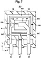
- the semiconductor device 201 is arranged with a first lead (collector lead) 21 which extends in a first direction (Y direction) having a die bonding region 21D in which a semiconductor element 1 is mounted, a second lead (gate lead) 22 which extends in the first direction and is adjacent to left side of the first lead 21, a third lead (emitter lead) 23 which extends in the first direction and is adjacent to the right side of the first lead, a bonding wire 31 which electrically connects the second lead and the bonding electrode 13G of the semiconductor element 1, a bonding wire 32 which electrically connects the third lead and a bonding area of the second electrode 13 of the semiconductor element 1, and a sealing body 4.
- the resistance and inductance component of a metal plate or an alloy plate is small compared to a wire.
- stress generated in a bonding part of the metal plate, allot plate and a bonding area is large.
- the mechanical strength in the bonding area of the second electrode 13 is high. Therefore, in the semiconductor device 201, the resistance and inductance component is reduced, and it is possible to prevent tears in the interlayer insulation film 12 and tears in the gate electrode 116.
- the first electrode on the back surface of the semiconductor element 1 is electrically and mechanically connected to the bonding region 21D of the first lead 21 via a conduction adhesive.
- the bonding wire 31 penetrates the aperture 142 which is formed on the protection film 14 of the semiconductor element 1 and is electrically connected to the bonding electrode 13G.
- the bonding wire 32 penetrates the aperture 141 which is formed on the protection film 14 above the substrate 10 and is electrically connected to the electrode 13.
- a wire of Au, Lu, Al for example can be practically used as the bonding wire 31 and 32 and it is possible to bond the wires using thermal compression and ultrasound vibration using a bonding device.
- An epoxy resin for example can be used as the sealing body 4.
- This epoxy resin is formed for example by a molding method.
- the bonding wires 31 and 32 and an inner part (one part) of each of the semiconductor 1, the first lead 21, the second lead 22 and the third lead 23 are air tight sealed within the sealing body 4.
- An outer part (one part) of each of the first lead 21, the second lead 22 and the third lead 23 projects out from the exterior of the sealing body 4.
- the planar structure of the interlayer insulation film 12 within the bonding area is formed in a mesh shape, and because the mechanical strength increases by the connection part 122, the extension part 121 adjacent in a second direction of the interlayer insulation film 12, bonding strength of the interlayer insulation film 12 when bonding is secured, and tears which occur in the interlayer insulation film 12 with bonding and breaks in an electrode (for example, the gate electrode 116 and the second electrode 13) are prevented.
- connection part 122 of the interlayer insulation film 12 is arranged at fixed intervals in the second direction, it is possible to sufficiently secure the planar area of the aperture 123. Therefore, because it is possible to sufficiently secure the contact area which is the original characteristic of the IGBT 11, it is possible to reduce an electric filed concentration, secure sufficient resistance and provide a semiconductor device 201 with the semiconductor element 1 which has good electrical characteristics.
- the planar shape of the interlayer insulation film 12 outside the bonding area is formed in a stripe shape, it is possible to secure the electrical characteristics of the semiconductor element 1 as stated previously.
- the semiconductor device 1 related to the first embodiment because it is possible to change the planar shape of the interlayer insulation film 12 for demonstrating these operation effects simply by changing the pattern of a manufacturing mask, there is no particular need to increase the number of manufacturing processes, and it is possible to reduce manufacturing costs. Furthermore, because it is not necessary to increase the thickness of the second electrode 13 and bonding electrode 13G for bonding, it is also possible to reduce manufacturing costs in this way.
- the planar shape particularly within the bonding area of the interlayer insulation film 12 of the IGBT 11, as is shown in Fig. 5 is formed by a mesh shape formed as needed so that an aperture 123 arranged at fixed intervals in the first direction and an aperture 123 which is adjacent in the second direction are on the same straight line. That is, the connection part 122 is formed in one straight line when seen in the second direction, and when seen in the first direction is formed repeatedly at fixed intervals, and the planar shape of the interlayer insulation film 12 related to the transformation example un offset the arrangement pitch of the connection part 122 and aperture 123.
- the planar shape of the interlayer insulation film 12 only within a bonding area of the semiconductor element 1 is formed in a mesh shape.
- the present invention is not limited to the type of structure and the planar shape of the interlayer insulation film within and outside the bonding area can be a mesh shape.
- the second embodiment of the present invention explains an example in which the present invention is applied to a power semiconductor device and manufacturing method of the semiconductor device mounted with a semiconductor element comprised of an IGBT having a planar structure.
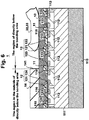
- the semiconductor element 1 mounted on the semiconductor device 201 related to the second embodiment, as shown in Fig. 6 is formed by an IGBT 11 having a planar structure. That is, the IGBT 11 is formed by arranging a collector region (p type second semiconductor region) 110, an n type base region (n type first semiconductor region or substrate) 111, a p type base region (p type first semiconductor region) 112, an emitter region (n type second semiconductor region) 113, a gate insulation film 115, a gate electrode 116, a collector electrode (first electrode) and an emitter electrode (second electrode) 13.
- a cross sectional structure of a basic semiconductor element 1 is the same as the cross sectional structure of the semiconductor element 1 of the semiconductor device 201 related to the first embodiment stated previously.
- the hole 114 shown in Fig. 1 is not arranged. That is, the semiconductor element 1, the gate electrode 116 is arranged with a planar structure via the gate insulation film 114 on the main surface of the base region 111, and a base region 112 and emitter region 113 are arranged by a double diffusion structure with the gate electrode 116 as a mask.
- the interlayer insulation film 12 is formed similar to the semiconductor device 201 related to the first embodiment shown in Fig. 1 to Fig. 4 stated previously, by a planar shaped extension part 121 having a stripe shape extending in the same direction as a first direction in which the gate electrode 118 extends, and arranged on the gate electrode at fixed intervals in a second direction the same as the arrangement intervals of the gate electrode 116, a planar shaped connection part 121 having a stripe shape, a connection part 122 which is connected with the extension part 121 adjacent in the second direction and formed as one unit, and an aperture 123 formed within a region surrounded by two extension parts 121 adjacent in the second direction and two connection parts 122 adjacent in the first direction. That is, the planar shape of the interlayer insulation 12 is formed in a mesh shape within at least the bonding area of the second electrode 13.
- the planar structure of the interlayer insulation film 12 within the bonding area of the second electrode 13 is formed in a mesh shape, and because the extension part 121 adjacent in the second direction of the interlayer insulation film 12 is connected with the connection part 122 and mechanical strength increases, the bonding strength of the interlayer insulation film 12 is secured when bonding and it is possible to prevent breaks in the interlayer insulation film 12 and breaks in an electrode (for example, gate electrode 116 or second electrode 13) that comes with bonding.
- an electrode for example, gate electrode 116 or second electrode 13
- connection part 122 of the interlayer insulation film 12 is arranged at fixed intervals in the second direction, it is possible to sufficiently secure the planar area (contact area) of the aperture 123. Therefore, because it is possible to sufficiently secure the contact area and current capacitance which is the original characteristic of the semiconductor element 1 having a stripe structure, it is possible to reduce an electric filed concentration, secure sufficient resistance and provide a semiconductor device 201 with the semiconductor element 1 which has good electrical characteristics.
- the semiconductor device 201 related to the second embodiment by forming the planar shape of the interlayer insulation film 12 outside the bonding area of the second electrode 13 in a stripe shape shown in Fig. 3 , it is possible to secure the electrical characteristics of the semiconductor element 1.
- the semiconductor device 201 related to the second embodiment because it is possible to change the planar shape of the interlayer insulation film 12 for demonstrating these operation effects simply by changing the pattern of a manufacturing mask, there is no particular need to increase the number of manufacturing processes, and it is possible to reduce manufacturing costs.
- the third embodiment of the present invention explains an example in which the connection method between the semiconductor element 1 with the second lead 22 and the third lead 23 is replaced in the semiconductor device 201 related to the first embodiment and the second embodiment stated previously.
- soldering paste 35 is used in each of the connections between the clip lead 22C and the bonding electrode 13G and the second clip lead 22, and each are electrically and mechanically connected.
- soldering paste 36 is used in each of the connections between the clip lead 23C and the second electrode 13 and the third clip lead 23, and each are electrically and mechanically connected.
- an alloy plate such as a Cu plate or an alloy plate such as a Fe ⁇ Ni plate for example for the clip lead 22C and the clip lead 23C.
- Pb ⁇ Sn solder or Pb free solder such as Sn- 3 wt % Ag ⁇ 0.5 wt % Cu for the soldering paste 35 and 36. Similar to the bonding of the bonding wire 31, a bonding method where thermal compression is combined with ultrasound vibrations is used in the connection of the clip lead 22 to the bonding electrode 13G via the soldering paste 35, and the connection of the clip lead 22C to the second lead 22 via the soldering paste 35.
- a bonding method which combines thermal compression with ultrasound vibrations similar to a heating method using a heater or bonding of the bonding wire 32, is used in the connection of the clip lead 23C to the second electrode 13 via the soldering paste 36, and the connection of the clip lead 23C to the third lead 23 via the soldering paste 36.
- a wetability improvement film can be formed on the surface of each of the bonding electrode 13G and the second electrode 13. It is possible to practically use a compound layer stacked with an Ni layer on a Ti layer for example as the wettability improvement film.
- the resistance and inductance component of a metal plate or alloy plate of the clip lead 22C and 23C is small compared to a wire. Reversely, stress generated at the bonding part between a metal plate or alloy plate and a bonding area is large.
- a connection part 122 is arranged on the interlayer insulation layer 12 in the bonding area of the second electrode 13 in the third embodiment, it is possible to increase mechanical strength in the bonding area of the second electrode 13. Therefore, in the semiconductor device 201 the resistance and inductance component can be reduced and it is possible to prevent tears in the interlayer insulation film and tears in the gate electrode 116.
- the fourth embodiment of the present invention explains an example in which the present invention is applied to a power semiconductor device and manufacturing method of the semiconductor device mounted with a semiconductor element comprised of an IGBT having a trench structure.
- the semiconductor element 1 (semiconductor chip) mounted in the semiconductor device related to the fourth embodiment includes a first edge 101 and a second edge 102 which face each other and extend in a second direction (X direction) and a third edge 103 and a fourth edge 104 which face each other and extend in a first direction (Y direction) which intersects the second direction, a first semiconductor region (substrate) 111 (specifically, refer to Fig. 11 and Fig.
- the aperture part 123 continues in order to pass through the third semiconductor region 113 with the interlayer insulation film 12 as a mask.
- a first width dimension 121W below the extension part 121 or in a second direction of the third semiconductor region 113 which contacts with the extension part 121 compared with a second width dimension 122W of the first direction of the third semiconductor region 113 which contacts with a connection part 122 below the connection part 122 is set large.
- Fig. 9 and Fig. 10 a first width dimension 121W below the extension part 121 or in a second direction of the third semiconductor region 113 which contacts with the extension part 121 compared with a second width dimension 122W of the first direction of the third semiconductor region 113 which contacts with a connection part 122 below the connection part 122 is set large.
- the first width dimension 121W of the third semiconductor region 113 is dimension from the end of the aperture part 123 side of the extension part 121 on the interlayer insulation film 12 to the gate electrode film 115.
- the second width dimension 122W of the third semiconductor region 113 is equivalent to the width dimension of the main surface side which contact with the third semiconductor region 113 of the connection part 112.
- the semiconductor element 1 is an IGBT 11 and this IGBT 11 is formed from an IGBT having a trench gate structure in the fourth embodiment as is shown in Fig. 11 and Fig. 2 . That is, the IGBT 11 is arranged with a p type fourth semiconductor region 110 which is a collector region (or drain region) (below called a collector region 110), a first semiconductor region 111 (below called base region 111) which is an n type base region and an n type first semiconductor region, a p type second semiconductor 112 which is a p type base region (called base region 112 below), an n type third semiconductor region 113 which is an emitter region (below called emitter region 113), a hole (trench) 114, a gate insulation film 115, a gate electrode 116, a collector electrode (first electrode) which is arranged on the entire bottom surface of the collector region 110, and an emitter electrode (second electrode) 13.
- gate electrode is used with the same meaning as the gate electrode explained in the first embodiment.
- the base region (substrate) 111 is formed with a planar shape having a first edge 101 and a second edge 102 opposing each other in the first direction and a third edge 104 and a fourth edge 104 opposing each other in second direction.
- the base region 111 in the manufacturing process of the semiconductor element 1, is cut out from a silicon single crystal wafer by a dicing process after manufacturing the IGBT (cell) 11, and is a semiconductor chip.
- the planar shape of the base region 111 is not always limited to this planar shape.
- the base region 111 may be formed by a planar rectangle in which the first edge 101 and the second edge 102 are long edges and the third edge 103 and the fourth edge 104 are short edges.
- first direction and second direction are used with the same meaning as the first direction and second direction explained in the first embodiment.
- the planar shape of the interlayer insulation layer 12 related to the fourth embodiment is a mesh shape which, within the bonding area of the first electrode 13, includes a plurality of extension parts 121 arranged at fixed intervals in the second direction and arranged between the second electrode 12 and gate electrode 116 which extend in the first direction, a connection part 122 which connects an adjacent connection part 121, and an aperture 123.
- the planar shape of the interlayer insulation film 12 outside of the bonding area of the first electrode 13 only the extension part 121 which is formed between the second electrode 13 and the gate electrode 116 has a stripe shape.
- the mesh shape of the interlayer insulation film 12 means a planar shaped extension part 121 having a stripe shape and arranged on the gate electrode 116 (hole 114), extending in the same direction as the first direction in which the gate electrode 116 extends and arranged at fixed intervals in the second direction the same as the gate electrode 116, a connecting part 122 formed as one part by linking with an adjacent extension part 121 in the second direction, and the aperture 123 formed in a region which is surrounded by two adjacent extension parts 121 in the second direction and two adjacent connecting parts 122 in the first direction.
- connection part 122 is connects adjacent extension parts 121 in the second direction at fixed intervals in the first direction, it is possible to improve the mechanical strength of the extension part 121 of the interlayer insulation film 12 and the gate electrode 116 directly below it within the bonding area of the second electrode 13. In particular, it is possible to prevent cracks and tears in the extension part 121 and the gate electrode 116 directly below it with respect to stress which is generated when bonding (for example, ultrasound vibration energy).
- the connecting part 122 of the interlayer insulation film 12 is arranged between adjacent extension parts 121 in the second direction, however, the connecting part 122 is arranged within the bonding area, and because aperture 123 is arranged as much as possible in a mesh shape also within the bonding area, it is possible to reduce contact area and current capacitance between the emitter 131 and the second electrode 13 and also prevent electrical field concentration.
- the manufacturing becomes easier and manufacturing costs do not increase.
- the fourth embodiment it is possible to practically use a silicon oxide film, specifically, a phosphosilicate glass (PSG) film as the interlayer insulation film 12, and the thickness of this phosphosilicate glass film is set at 0.5 ⁇ m to 3.0 ⁇ m for example.
- PSG phosphosilicate glass
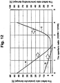
- Fig. 12 the causal relationship between the aperture ratio and the defect ratio of the aperture 123 of the interlayer insulation film 12 is shown in Fig. 12 .
- the horizontal axis shows the aperture ratio of the aperture 123 of the interlayer insulation film 12
- the left vertical axis shows the defect ratio (%) due to avalanche damage
- the right vertical axis shows the defect ratio (%) due to wire bonding damage.
- the aperture ratio of the aperture 123 of the interlayer insulation film 12 increases, that is, when the second width dimension 122W of the connection part 122 increases with respect to the first width dimension 121W of the extension part 121, it is possible to reduce the defect ratio caused by wire bonding damage.
- the defect ratio effectively becomes 0 (zero) when the aperture ratio is 2.2 in the curve A and the aperture ratio in the curve B is 2.0 shown in Fig. 12 . That is, it is possible to prevent cracks and tears in the extension part 121 of the interlayer insulation film 12 and the gate electrode 116 directly below it.
- the wire bonding conditions of curve A are the bonding load is 1200 g/cm 2 , ultrasound vibration energy (ultrasound power) is 145 Hz at a first side, and 190 Hz at a second side, and the ultrasound vibration time is 120 msec at the first side and 170 msec at the second side.
- the wire bonding conditions of curve B are the bonding load is 1200 glcm 2 , ultrasound vibration energy (ultrasound power) is 145 Hz at a first side, and 180 Hz at a second side, and the ultrasound vibration time is 120 msec at the first side and 170 msec at the second side.
- the aperture ratio of the aperture 123 of the interlayer insulation film 122 increases, that is when the second width dimension 122W of the connection part 122 increases with respect to the first width dimension 121W of the extension part 121 increases, the defect ratio caused by avalanche damage increases when the aperture ratio is 2.6 as a border as is shown in the curve C.
- a current path is shortest from a bonding wire on the region in which the third semiconductor region 113 is exposed.
- the current path becomes longer from the center (for example, shown by K in Fig. 10 ) of the connection part 122 to the third semiconductor 113 and the dynamic time lag of a current becomes larger.
- the amount of avalanche tolerance it is important that the energy which is applied is diffused over a larger area, the current concentration is relaxed and a parasitic transistor is not switched ON. Within this, lowering the resistance of the second semiconductor region 112 directly below the third semiconductor region 113 is effective. Because etching is performed until one part of the third semiconductor region 113 is passed through with the interlayer insulation film as a mask, the aperture 123 and the resistance of the second semiconductor region 112 directly below the third semiconductor region 113 has a close relationship. That is, based on the causal relationship shown in Fig.
- the planar shape of the interlayer insulation film 12 is adopted so that a mesh shape in which the aperture 123 arranged at fixed intervals in the first direction and an aperture 123 adjacent in a second direction are offset.
- the amount of offset is half an arrangement pitch for example.
- bonding area of the second electrode 12 in which the planar shape of the interlayer insulation film is set in a mesh shape means a region in which a bonding wire (32) which electrically connects the second electrode (emitter electrode) 13 and an emitter lead (external terminal) is bonded.
- a protection film 14 is arranged on the second electrode 13, an aperture 141 for electrically connecting the bonding wire (32) with the second electrode 13 is arranged on the protection film 14 as is shown in Fig. 11 , and the bonding area of the second electrode 13 is within a region of the aperture 141 set in the protection film 14.
- the planar shape of the interlayer insulation film 12 outside the bonding area of the second electrode 13 is a stripe shape.
- the interlayer insulation film 12 is arranged with a plurality of planar shaped extension part 121 having a stripe shape arranged above gate electrode 116 (or hole 114) extending in the same direction as the first direction in which the gate electrode 115 extends and arranged at fixed intervals in a second direction the same as the arrangement direction of the gate electrode 116, and a plurality of aperture parts 124 having a planar shape sandwiched between adjacent extension parts 121 in the second direction and arranged at firs intervals in the second direction.
- connection part 122 between adjacent extension parts 121 in the second direction.
- connection part 122 because it is possible to increase the aperture area of the aperture part 124, it is possible to secure contact area and current capacitance between the emitter region 113 and the second electrode 13 and prevent electric field concentration.
- the second electrode (emitter electrode) 13 is arranged on the interlayer insulation film 12 and within the bonding area of the second electrode 13, the second electrode 13 is connected to the IGBT 11 via the aperture 123 of the interlayer insulation film 12, Outside the bonding area of the second electrode 13, the second electrode is connected to the IGBT 11 via the aperture 124 of the interlayer insulation film 12.
- the second electrode 13 is used as an emitter electrode (or source electrode) and a aluminum alloy film for example can be used as the second electrode 13.
- the aluminum alloy film is an aluminum added with additives such as Si for preventing alloy spike, or Cu for preventing migration.
- the protection film 14 is arranged on the second electrode 13 in the entire region above the main surface of the substrate 10. In an element region, the aperture 141 is arranged in a bonding area of the second electrode 13. In addition, as is shown in Fig. 4 , in the protection film 14, in an element region, the bonding electrode 13G for connecting to the gate electrode 116 of the IGBT 11 is exposed by the aperture 142 of the protection film 14. The bonding electrode 13G of the gate electrode 116 is formed by the same conduction material in the same conduction layer as the second electrode 13. The aperture 141 of the protection film 14 is arranged at the center part of the base region (substrate) 111 as is shown in Fig.
- the aperture 142 is arranged near the third edge 103 of the base region 111.
- the planar area of the aperture 142 is small compared to the planar area of the aperture 141. It is possible to practically use a resin film such as PIF (polyimide ⁇ film) or PSG film for example as the protection film 14.
- the semiconductor device 201 related to the fourth embodiment is arranged with a semiconductor element 1, a first lead (collector external terminal) 21 which extends in a first direction (X direction) having a die bonding region 21D in which a semiconductor element 1 is mounted, a second lead (gate external terminal) 22 which extends in the first direction and is arranged to left side of the first lead 21, a third lead (emitter external terminal) 23 which extends in the first direction and is arranged to the right side of the first lead, a bonding wire 31 which electrically connects the second lead and the bonding electrode 13G of the semiconductor element 1, a bonding wire 32 which electrically connects the third lead and a bonding area of the second electrode 13 of the semiconductor element 1, and a sealing body 4.
- Ni plating may also be used on the surface of the Cu plate.
- the first electrode of the back surface of the semiconductor element 1 is electrically and mechanically connected to the die bonding region 21D of the first lead 21 via a conduction adhesive.
- the bonding wire 31 is electrically connected to the bonding region 13G via the aperture 142 which is formed on the protection film 14 of the semiconductor element 1.
- the bonding wire 32 is electrically connected to the electrode 13 via the aperture 141 which is formed on the protection film above the substrate 10.
- a wire of Au, Lu, Al can be practically used as the bonding wire 31, 32 and this wire is bonded by combining thermal compression with ultrasound vibrations used a bonding device.
- An epoxy resin for example can be used as the sealing body 4.
- This epoxy resin is formed for example by a molding method.
- An inner part (one part) of each of the semiconductor 1m the first lead 21, the second lead 22 and the third lead 23 and the bonding wires 31, 32 are air tight sealed within the sealing body 4.
- An outer part (one part) of each of the first lead 21, the second lead 22 and the third lead 23 projects out from the exterior of the sealing body 4.
- the assembly sequence of the semiconductor device 201 is as follows. First, the semiconductor element 1 is manufactured formed with the IGBT 11, interlayer insulation film 12, second electrode 13 and protection film 14 in this order. Next, the semiconductor element 1 is installed on the die bonding region 21D of the first lead 21. Next, the bonding wires 31 and 32 are bonded. Then, the semiconductor device 201 related to the fourth embodiment is completed by molding the semiconductor element 1 by the sealing body 4.
- the planar structure of the interlayer insulation film 12 within the bonding area is formed in a mesh shape, and because the mechanical strength increases by the connection part 122, the extension part 121 adjacent in a second direction of the interlayer insulation film 12, bonding strength of the interlayer insulation film 12 when bonding is secured, and tears which occur in the interlayer insulation film 12 with bonding and breaks in an electrode (for example, the gate electrode 116 and the second electrode 13) are prevented.
- connection part 122 of the interlayer insulation film 12 is arranged at fixed intervals in the second direction, it is possible to sufficiently secure the planar area of the aperture 123. Therefore, because it is possible to sufficiently secure the contact area which is the original characteristic of the IGBT 11, it is possible to reduce an electric filed concentration, secure sufficient resistance and provide a semiconductor device 201 with the semiconductor element 1 which has good electrical characteristics.
- the ratio between the first width dimension 121W below the extension part 121 (or the extension part 121) of the third semiconductor region 113, and the second width dimension 122W below the connection part (or the connection part 122) of the third semiconductor region 113 is set within an appropriate range, it is possible to secure the bonding strength of the interlayer insulation film 12 when bonding and secure sufficient resistance.
- the planar shape of the interlayer insulation film 12 outside the bonding area is formed in a stripe shape, it is possible to secure the electrical characteristics of the semiconductor element 1 as stated previously.
- the semiconductor device 1 related to the fourth embodiment because it is possible to change the planar shape of the interlayer insulation film 12 for demonstrating these operation effects simply by changing the pattern of a manufacturing mask, there is no particular need to increase the number of manufacturing processes, and it is possible to reduce manufacturing costs. Furthermore, because it is not necessary to increase the thickness of the second electrode 13 and bonding electrode 13G for bonding, it is also possible to reduce manufacturing costs in this way.
- the planar shape particularly within the bonding area of the interlayer insulation film 12 of the IGBT 11, similar to the semiconductor device 201 related to the first embodiment shown in Fig. 8 , is formed as needed by a mesh shape so that an aperture 123 arranged at fixed intervals in the first direction and an aperture 123 which is adjacent in the second direction are on the same straight line. That is, the connection part 122 is formed in one straight line when seen in the second direction, and when seen in the first direction is formed repeatedly at fixed intervals, and the planar shape of the interlayer insulation film 12 related to the transformation example un-offset the arrangement pitch of the connection part 122 and aperture 123.
- the planar shape of the interlayer insulation film 12 only within a bonding area of the semiconductor element 1 is formed in a mesh shape.
- the present invention is not limited to the type of structure and the planar shape of the interlayer insulation film within and outside the bonding area can be a mesh shape.
- the fifth embodiment of the present invention is a transformation example of a power semiconductor device and manufacturing method of the semiconductor device related to the fourth embodiment and explains an example in which the present invention is applied to a power semiconductor device and manufacturing method of the semiconductor device mounted with a semiconductor element comprised of an IGBT having a planar structure.
- the semiconductor element 1 mounted on the semiconductor device 201 related to the fifth embodiment, as shown in Fig. 13 is formed by an IGBT 11 having a planar structure. That is, the IGBT 11 is formed by arranging a collector region (p type fourth semiconductor region) 110, an n type base region (n type second semiconductor region or substrate) 111, a p type base region (p type second semiconductor region) 112, an emitter region (n type third semiconductor region) 113, a gate insulation film 115, a gate electrode 116, a collector electrode (first electrode) and an emitter electrode (second electrode) 13.
- a cross sectional structure of a basic semiconductor element 1 is the same as the cross sectional structure of the semiconductor element 1 of the semiconductor device 201 related to the fourth embodiment stated previously.
- the hole 114 shown in Fig. 9 and Fig. 10 is not arranged. That is, in the semiconductor element 1, the gate electrode 116 is arranged with a planar structure via the gate insulation film 114 on the main surface of the base region 111, and a base region 112 and emitter region 113 are arranged by a double diffusion structure with the gate electrode 116 as a mask.
- the sixth embodiment of the present invention explains an example in which the connection method between the semiconductor element 1 with the second lead 22 and the third lead 23 is replaced in the semiconductor device 201 related to the fourth embodiment and the fifth embodiment stated previously.
- soldering paste 35 is used in each of the connections between the clip lead 22C and the bonding electrode 13G and the second clip lead 22, and each are electrically and mechanically connected.
- soldering paste 35 is used in each of the connections between the clip lead 23C and the second electrode 13 and the third clip lead 23, and each are electrically and mechanically connected.
- an alloy plate such as a Cu plate or an alloy plate such as a Fe-Ni plate for example for the clip lead 22C and the clip lead 23C.
- Pb ⁇ Sn solder or Pb free solder such as Sn ⁇ 3 wt % Ag ⁇ 0.5 wt % Cu for the soldering paste 35 and 36. Similar to the bonding of the bonding wire 31, a bonding method where thermal compression is combined with ultrasound vibrations is used in the connection of the clip lead 22 to the bonding electrode 13G via the soldering paste 35, and the connection of the clip lead 22C to the second lead 22 via the soldering paste 35.
- a bonding method which combines thermal compression with ultrasound vibrations similar to a heating method using a heater or bonding of the bonding wire 32, is used in the connection of the clip lead 23C to the second electrode 13 via the soldering paste 36, and the connection of the clip lead 23C to the third lead 23 via the soldering paste 36.
- a wetability improvement film can be formed on the surface of each of the bonding electrode 13G and the second electrode 13. It is possible to practically use a compound layer stacked with an Ni layer on a Ti layer for example as the wettability improvement film.
- the resistance and inductance component of a metal plate or alloy plate of the clip lead 22C and 23C is small compared to a wire. Reversely, stress generated at the bonding part between a metal plate or alloy plate and a bonding area is large.
- a connection part 122 is arranged on the interlayer insulation layer 12 in the bonding area of the second electrode 13 in the sixth embodiment, it is possible to increase mechanical strength in the bonding area of the second electrode 13. Therefore, in the semiconductor device 201 the resistance and inductance component can be reduced and it is possible to prevent tears in the interlayer insulation film and tears in the gate electrode 116.
- the present invention can be applied to various alternative forms, embodiments and technologies.
- an example of the semiconductor device 201 mounted with the semiconductor element 1 comprised of the IGBT 11 the present invention is not limited to the IGBT 11.
- the present invention can also be applied to a semiconductor element comprised of a power transistor having not only a trench structure but also a planar structure and a semiconductor device mounted with this semiconductor element.
- the corner part of the aperture 123 of the interlayer insulation film 123 may be round.
- the present invention can be widely used in a semiconductor device and manufacturing method of the semiconductor device in which it is necessary to prevent damage of interlayer insulation film and damage of an electrode which is generated with bonding while securing bonding strength.
- the present invention can be widely used in a semiconductor device and manufacturing method of the semiconductor device in which it is necessary to prevent damage of interlayer insulation film and damage of an electrode which is generated with bonding while comparatively securing damage tolerance and bonding strength.
- the present invention can be widely used in a semiconductor device and manufacturing method of the semiconductor device in which it is necessary to improve the electrical characteristics of a semiconductor element.
- the present invention can be widely used in a semiconductor device and manufacturing method of the semiconductor device in which it is necessary to reduce manufacturing costs.
Landscapes
- Internal Circuitry In Semiconductor Integrated Circuit Devices (AREA)
- Bipolar Transistors (AREA)
Claims (4)
- Halbleitervorrichtung, die umfasst:ein Substrat (111) mit einer ersten Kante (101) und einer zweiten Kante (102), die einander in einer ersten Richtung gegenüberliegen, sowie einer dritten Kante (103) und einer vierten Kante (104), die einander in einer zweiten Richtung gegenüberliegen, die die erste Richtung schneidet;eine Vielzahl erster Halbleiterbereiche (112), die sich in der ersten Richtung erstrecken, auf dem Substrat (111) in der zweiten Richtung angeordnet sind und eine erste Leitfähigkeit aufweisen;eine Vielzahl zweiter Halbleiterbereiche (113), die sich in der ersten Richtung erstrecken, an den Rändern der ersten Halbleiterbereiche (112) in der zweiten Richtung innerhalb des ersten Halbleiterbereiches (112) angeordnet sind und eine zweite Leitfähigkeit aufweisen;eine Vielzahl von Steuerelektroden (116), die zwischen benachbarten zweiten Halbleiterbereichen (113) angeordnet sind, wobei sich die Steuerelektroden (116) in der ersten Richtung erstrecken und in Reihen angeordnet sind, die in der zweiten Richtung beabstandet sind;einen Zwischenschicht-Isolierfilm (12), der eine Vielzahl von Verlängerungsteilen (121), Verbindungsteilen (122) sowie Öffnungen (123) einschließt, wobei sich die Verlängerungsteile (121) in der ersten Richtung erstrecken und die unter ihnen angeordneten Steuerelektroden (116) abdecken; die Verbindungsteile (122) benachbarte Verlängerungsteile (121) verbinden und die Öffnungen (123) wenigstens einen Teil einer Oberfläche der ersten Halbleiterbereiche (112) sowie wenigstens einen Teil einer Oberfläche der zweiten Halbleiterbereiche (113) freilegen und eine Form haben, die durch die Verlängerungsteile (121) sowie die Verbindungsteile (122) bestimmt wird, und in Reihen in der ersten Richtung angeordnet sind;eine Elektrode (13), die auf dem Zwischenschicht-Isolierfilm (12) angeordnet ist und die ersten Halbleiterbereiche (112) und die zweiten Halbleiterbereiche (113) über die Öffnungen (123) des Zwischenschicht-Isolierfilms (12) elektrisch verbindet,wobei die Steuerelektroden (116) in einer Streifenform in der ersten Richtung ausgebildet sind und der Zwischenschicht-Isolierfilm (12) innerhalb eines Verbindungsbereiches der Elektrode (13) in einer Netzform ausgebildet ist.
- Halbleitervorrichtung nach Anspruch 1, die des Weiteren umfasst:Löcher (114), die sich jeweils in der ersten Richtung erstrecken und in Reihen angeordnet sind, die in der zweiten Richtung beabstandet sind; sowieIsolierfilme (115), die jeweils an einer Seitenfläche und einer Bodenfläche jedes der Löcher (114) angeordnet sind;wobei die Steuerelektroden (116) in den Löchern (114) eingebettet sind und der Isolierfilm (115) jeweils zwischen der Steuerelektrode (116) und der Seiten- sowie der Bodenfläche jedes der Löcher (114) angeordnet ist.
- Halbleitervorrichtung nach Anspruch 1, wobei sich außerhalb des Verbindungsbereiches die Zwischenschicht-Isolierfilme (12) in der ersten Richtung erstrecken, in festen Abständen in der zweiten Richtung angeordnet sind, frei von den Verbindungsteilen (122) sind und die Form von Streifen haben.
- Halbleitervorrichtung nach Anspruch 1, wobei eine externe Verdrahtung (22, 23) eines Leiters oder einer Klemmleitung (22C, 23C) elektrisch mit der Elektrode (13) verbunden ist.
Applications Claiming Priority (3)
| Application Number | Priority Date | Filing Date | Title |
|---|---|---|---|
| JP2007291892A JP4293272B2 (ja) | 2007-11-09 | 2007-11-09 | 半導体装置 |
| JP2007328672A JP5098630B2 (ja) | 2007-12-20 | 2007-12-20 | 半導体装置及びその製造方法 |
| PCT/JP2008/067009 WO2009060670A1 (ja) | 2007-11-09 | 2008-09-19 | 半導体装置及びその製造方法 |
Publications (3)
| Publication Number | Publication Date |
|---|---|
| EP2209142A1 EP2209142A1 (de) | 2010-07-21 |
| EP2209142A4 EP2209142A4 (de) | 2010-11-10 |
| EP2209142B1 true EP2209142B1 (de) | 2020-05-27 |
Family
ID=40625572
Family Applications (1)
| Application Number | Title | Priority Date | Filing Date |
|---|---|---|---|
| EP08847499.4A Active EP2209142B1 (de) | 2007-11-09 | 2008-09-19 | Halbleiterbauelement und herstellungsverfahren dafür |
Country Status (4)
| Country | Link |
|---|---|
| US (1) | US8207612B2 (de) |
| EP (1) | EP2209142B1 (de) |
| CN (1) | CN101821853B (de) |
| WO (1) | WO2009060670A1 (de) |
Families Citing this family (18)
| Publication number | Priority date | Publication date | Assignee | Title |
|---|---|---|---|---|
| WO2010125639A1 (ja) * | 2009-04-28 | 2010-11-04 | 三菱電機株式会社 | 電力用半導体装置 |
| JP6099302B2 (ja) * | 2011-10-28 | 2017-03-22 | 富士電機株式会社 | 半導体装置の製造方法 |
| WO2013067270A1 (en) * | 2011-11-04 | 2013-05-10 | Invensas Corporation | Bonding wedge |
| CN103151251B (zh) * | 2011-12-07 | 2016-06-01 | 无锡华润华晶微电子有限公司 | 沟槽型绝缘栅双极型晶体管及其制备方法 |
| US9306046B2 (en) * | 2012-02-22 | 2016-04-05 | Mitsubishi Electric Corporation | Semiconductor device having a semiconductor element and a terminal connected to the semiconductor element |
| CN104124271B (zh) * | 2013-04-28 | 2017-09-12 | 三垦电气株式会社 | 半导体装置 |
| JP5729497B1 (ja) * | 2014-02-04 | 2015-06-03 | トヨタ自動車株式会社 | 半導体装置及び半導体装置の製造方法 |
| DE102014107387A1 (de) * | 2014-05-26 | 2015-11-26 | Infineon Technologies Ag | Halbleiterchip mit verbesserter bondbarkeit und verfahren zur herstellung einer bondverbindung |
| US9722059B2 (en) * | 2015-08-21 | 2017-08-01 | Infineon Technologies Ag | Latch-up free power transistor |
| DE102016116273B4 (de) * | 2016-08-31 | 2024-07-18 | Infineon Technologies Austria Ag | Halbleiterbauelement und Verfahren zum Bilden eines Halbleiterbauelements |
| WO2018225571A1 (ja) * | 2017-06-09 | 2018-12-13 | 富士電機株式会社 | 半導体装置および半導体装置の製造方法 |
| WO2019049572A1 (ja) | 2017-09-05 | 2019-03-14 | 富士電機株式会社 | 炭化珪素半導体装置および炭化珪素半導体装置の製造方法 |
| US10354871B2 (en) * | 2017-09-11 | 2019-07-16 | General Electric Company | Sputtering system and method for forming a metal layer on a semiconductor device |
| JP7106981B2 (ja) * | 2018-05-18 | 2022-07-27 | 富士電機株式会社 | 逆導通型半導体装置 |
| JP7246287B2 (ja) * | 2019-09-13 | 2023-03-27 | 株式会社東芝 | 半導体装置およびその製造方法 |
| EP3907758A1 (de) * | 2020-05-08 | 2021-11-10 | Infineon Technologies AG | Halbleiterchip, halbleiterschaltungsanordnung und verfahren zur herstellung |
| JP7663029B2 (ja) * | 2021-06-11 | 2025-04-16 | 株式会社デンソー | 半導体装置 |
| JP7577623B2 (ja) * | 2021-07-12 | 2024-11-05 | ルネサスエレクトロニクス株式会社 | 半導体装置 |
Family Cites Families (9)
| Publication number | Priority date | Publication date | Assignee | Title |
|---|---|---|---|---|
| US4906588A (en) * | 1988-06-23 | 1990-03-06 | Dallas Semiconductor Corporation | Enclosed buried channel transistor |
| JP2944840B2 (ja) * | 1993-03-12 | 1999-09-06 | 株式会社日立製作所 | 電力用半導体装置 |
| JPH1022322A (ja) * | 1996-06-28 | 1998-01-23 | Denso Corp | 半導体装置 |
| US6472678B1 (en) * | 2000-06-16 | 2002-10-29 | General Semiconductor, Inc. | Trench MOSFET with double-diffused body profile |
| JP4221904B2 (ja) | 2001-01-29 | 2009-02-12 | 富士電機デバイステクノロジー株式会社 | 半導体装置およびその製造方法 |
| US6921699B2 (en) * | 2002-09-30 | 2005-07-26 | International Rectifier Corporation | Method for manufacturing a semiconductor device with a trench termination |
| JP2005303218A (ja) | 2004-04-16 | 2005-10-27 | Renesas Technology Corp | 半導体装置およびその製造方法 |
| JP2006140263A (ja) * | 2004-11-11 | 2006-06-01 | Sanken Electric Co Ltd | 半導体素子及び半導体素子の製造方法 |
| JP4609656B2 (ja) | 2005-12-14 | 2011-01-12 | サンケン電気株式会社 | トレンチ構造半導体装置 |
-
2008
- 2008-09-19 US US12/682,383 patent/US8207612B2/en active Active
- 2008-09-19 EP EP08847499.4A patent/EP2209142B1/de active Active
- 2008-09-19 WO PCT/JP2008/067009 patent/WO2009060670A1/ja not_active Ceased
- 2008-09-19 CN CN2008801110162A patent/CN101821853B/zh active Active
Non-Patent Citations (1)
| Title |
|---|
| None * |
Also Published As
| Publication number | Publication date |
|---|---|
| CN101821853B (zh) | 2012-06-27 |
| EP2209142A4 (de) | 2010-11-10 |
| WO2009060670A1 (ja) | 2009-05-14 |
| US8207612B2 (en) | 2012-06-26 |
| CN101821853A (zh) | 2010-09-01 |
| US20100264546A1 (en) | 2010-10-21 |
| EP2209142A1 (de) | 2010-07-21 |
Similar Documents
| Publication | Publication Date | Title |
|---|---|---|
| EP2209142B1 (de) | Halbleiterbauelement und herstellungsverfahren dafür | |
| CN102194806B (zh) | 堆栈式双晶片封装及其制备方法 | |
| US8154129B2 (en) | Electrode structure and semiconductor device | |
| KR20080096483A (ko) | 반도체 장치 | |
| US8754510B2 (en) | Conduction path, semiconductor device using the same, and method of manufacturing conduction path, and semiconductor device | |
| US9355953B2 (en) | Vertical semiconductor MOSFET device with double substrate-side multiple electrode connections and encapsulation | |
| TW200947651A (en) | Semiconductor device | |
| EP2546869B1 (de) | Halbleitervorrichtung mit als verbindungsmaterialfliesssperren wirkenden drahtelementen und entsprechendes herstellungsverfahren | |
| JP2008518445A (ja) | 炭化ケイ素デバイス用のはんだ付け可能上部金属 | |
| US20230238307A1 (en) | Dual-side cooling semiconductor packages and related methods | |
| KR100477568B1 (ko) | 반도체 패키지 및 그 제조방법 | |
| JP5098630B2 (ja) | 半導体装置及びその製造方法 | |
| US7847316B2 (en) | Semiconductor device and its manufacture | |
| US7253507B2 (en) | Semiconductor device | |
| JP4293272B2 (ja) | 半導体装置 | |
| KR20220044502A (ko) | 반도체 장치 | |
| US9601572B2 (en) | Semiconductor device for reducing gate wiring length | |
| JP7383881B2 (ja) | 半導体装置および半導体装置の製造方法 | |
| US11302612B2 (en) | Lead frame wiring structure and semiconductor module | |
| US20240297118A1 (en) | Semiconductor element and semiconductor device | |
| JP7665974B2 (ja) | 半導体装置および半導体装置の製造方法 | |
| US20240355738A1 (en) | Power Semiconductor Devices Including Beryllium Metallization | |
| US12191264B2 (en) | Thermal performance improvement and stress reduction in semiconductor device modules | |
| EP3907758A1 (de) | Halbleiterchip, halbleiterschaltungsanordnung und verfahren zur herstellung |
Legal Events
| Date | Code | Title | Description |
|---|---|---|---|
| PUAI | Public reference made under article 153(3) epc to a published international application that has entered the european phase |
Free format text: ORIGINAL CODE: 0009012 |
|
| 17P | Request for examination filed |
Effective date: 20100409 |
|
| AK | Designated contracting states |
Kind code of ref document: A1 Designated state(s): AT BE BG CH CY CZ DE DK EE ES FI FR GB GR HR HU IE IS IT LI LT LU LV MC MT NL NO PL PT RO SE SI SK TR |
|
| AX | Request for extension of the european patent |
Extension state: AL BA MK RS |
|
| A4 | Supplementary search report drawn up and despatched |
Effective date: 20101013 |
|
| DAX | Request for extension of the european patent (deleted) | ||
| 17Q | First examination report despatched |
Effective date: 20110727 |
|
| REG | Reference to a national code |
Ref country code: DE Ref legal event code: R079 Ref document number: 602008062776 Country of ref document: DE Free format text: PREVIOUS MAIN CLASS: H01L0029780000 Ipc: H01L0023000000 |
|
| RIC1 | Information provided on ipc code assigned before grant |
Ipc: H01L 29/739 20060101ALI20191127BHEP Ipc: H01L 21/60 20060101ALI20191127BHEP Ipc: H01L 23/52 20060101ALI20191127BHEP Ipc: H01L 23/00 20060101AFI20191127BHEP Ipc: H01L 29/78 20060101ALI20191127BHEP Ipc: H01L 29/417 20060101ALI20191127BHEP Ipc: H01L 23/495 20060101ALI20191127BHEP Ipc: H01L 21/336 20060101ALI20191127BHEP Ipc: H01L 29/06 20060101ALI20191127BHEP |
|
| GRAP | Despatch of communication of intention to grant a patent |
Free format text: ORIGINAL CODE: EPIDOSNIGR1 |
|
| STAA | Information on the status of an ep patent application or granted ep patent |
Free format text: STATUS: GRANT OF PATENT IS INTENDED |
|
| INTG | Intention to grant announced |
Effective date: 20200117 |
|
| GRAS | Grant fee paid |
Free format text: ORIGINAL CODE: EPIDOSNIGR3 |
|
| GRAA | (expected) grant |
Free format text: ORIGINAL CODE: 0009210 |
|
| STAA | Information on the status of an ep patent application or granted ep patent |
Free format text: STATUS: THE PATENT HAS BEEN GRANTED |
|
| AK | Designated contracting states |
Kind code of ref document: B1 Designated state(s): AT BE BG CH CY CZ DE DK EE ES FI FR GB GR HR HU IE IS IT LI LT LU LV MC MT NL NO PL PT RO SE SI SK TR |
|
| REG | Reference to a national code |
Ref country code: GB Ref legal event code: FG4D |
|
| REG | Reference to a national code |
Ref country code: CH Ref legal event code: EP |
|
| REG | Reference to a national code |
Ref country code: DE Ref legal event code: R096 Ref document number: 602008062776 Country of ref document: DE |
|
| REG | Reference to a national code |
Ref country code: AT Ref legal event code: REF Ref document number: 1275451 Country of ref document: AT Kind code of ref document: T Effective date: 20200615 |
|
| REG | Reference to a national code |
Ref country code: LT Ref legal event code: MG4D |
|
| PG25 | Lapsed in a contracting state [announced via postgrant information from national office to epo] |
Ref country code: SE Free format text: LAPSE BECAUSE OF FAILURE TO SUBMIT A TRANSLATION OF THE DESCRIPTION OR TO PAY THE FEE WITHIN THE PRESCRIBED TIME-LIMIT Effective date: 20200527 Ref country code: NO Free format text: LAPSE BECAUSE OF FAILURE TO SUBMIT A TRANSLATION OF THE DESCRIPTION OR TO PAY THE FEE WITHIN THE PRESCRIBED TIME-LIMIT Effective date: 20200827 Ref country code: IS Free format text: LAPSE BECAUSE OF FAILURE TO SUBMIT A TRANSLATION OF THE DESCRIPTION OR TO PAY THE FEE WITHIN THE PRESCRIBED TIME-LIMIT Effective date: 20200927 Ref country code: GR Free format text: LAPSE BECAUSE OF FAILURE TO SUBMIT A TRANSLATION OF THE DESCRIPTION OR TO PAY THE FEE WITHIN THE PRESCRIBED TIME-LIMIT Effective date: 20200828 Ref country code: FI Free format text: LAPSE BECAUSE OF FAILURE TO SUBMIT A TRANSLATION OF THE DESCRIPTION OR TO PAY THE FEE WITHIN THE PRESCRIBED TIME-LIMIT Effective date: 20200527 Ref country code: PT Free format text: LAPSE BECAUSE OF FAILURE TO SUBMIT A TRANSLATION OF THE DESCRIPTION OR TO PAY THE FEE WITHIN THE PRESCRIBED TIME-LIMIT Effective date: 20200928 Ref country code: LT Free format text: LAPSE BECAUSE OF FAILURE TO SUBMIT A TRANSLATION OF THE DESCRIPTION OR TO PAY THE FEE WITHIN THE PRESCRIBED TIME-LIMIT Effective date: 20200527 |
|
| REG | Reference to a national code |
Ref country code: NL Ref legal event code: MP Effective date: 20200527 |
|
| PG25 | Lapsed in a contracting state [announced via postgrant information from national office to epo] |
Ref country code: LV Free format text: LAPSE BECAUSE OF FAILURE TO SUBMIT A TRANSLATION OF THE DESCRIPTION OR TO PAY THE FEE WITHIN THE PRESCRIBED TIME-LIMIT Effective date: 20200527 Ref country code: BG Free format text: LAPSE BECAUSE OF FAILURE TO SUBMIT A TRANSLATION OF THE DESCRIPTION OR TO PAY THE FEE WITHIN THE PRESCRIBED TIME-LIMIT Effective date: 20200827 Ref country code: HR Free format text: LAPSE BECAUSE OF FAILURE TO SUBMIT A TRANSLATION OF THE DESCRIPTION OR TO PAY THE FEE WITHIN THE PRESCRIBED TIME-LIMIT Effective date: 20200527 |
|
| REG | Reference to a national code |
Ref country code: AT Ref legal event code: MK05 Ref document number: 1275451 Country of ref document: AT Kind code of ref document: T Effective date: 20200527 |
|
| PG25 | Lapsed in a contracting state [announced via postgrant information from national office to epo] |
Ref country code: NL Free format text: LAPSE BECAUSE OF FAILURE TO SUBMIT A TRANSLATION OF THE DESCRIPTION OR TO PAY THE FEE WITHIN THE PRESCRIBED TIME-LIMIT Effective date: 20200527 |
|
| PG25 | Lapsed in a contracting state [announced via postgrant information from national office to epo] |
Ref country code: AT Free format text: LAPSE BECAUSE OF FAILURE TO SUBMIT A TRANSLATION OF THE DESCRIPTION OR TO PAY THE FEE WITHIN THE PRESCRIBED TIME-LIMIT Effective date: 20200527 Ref country code: EE Free format text: LAPSE BECAUSE OF FAILURE TO SUBMIT A TRANSLATION OF THE DESCRIPTION OR TO PAY THE FEE WITHIN THE PRESCRIBED TIME-LIMIT Effective date: 20200527 Ref country code: DK Free format text: LAPSE BECAUSE OF FAILURE TO SUBMIT A TRANSLATION OF THE DESCRIPTION OR TO PAY THE FEE WITHIN THE PRESCRIBED TIME-LIMIT Effective date: 20200527 Ref country code: CZ Free format text: LAPSE BECAUSE OF FAILURE TO SUBMIT A TRANSLATION OF THE DESCRIPTION OR TO PAY THE FEE WITHIN THE PRESCRIBED TIME-LIMIT Effective date: 20200527 Ref country code: RO Free format text: LAPSE BECAUSE OF FAILURE TO SUBMIT A TRANSLATION OF THE DESCRIPTION OR TO PAY THE FEE WITHIN THE PRESCRIBED TIME-LIMIT Effective date: 20200527 Ref country code: ES Free format text: LAPSE BECAUSE OF FAILURE TO SUBMIT A TRANSLATION OF THE DESCRIPTION OR TO PAY THE FEE WITHIN THE PRESCRIBED TIME-LIMIT Effective date: 20200527 Ref country code: IT Free format text: LAPSE BECAUSE OF FAILURE TO SUBMIT A TRANSLATION OF THE DESCRIPTION OR TO PAY THE FEE WITHIN THE PRESCRIBED TIME-LIMIT Effective date: 20200527 |
|
| PG25 | Lapsed in a contracting state [announced via postgrant information from national office to epo] |
Ref country code: PL Free format text: LAPSE BECAUSE OF FAILURE TO SUBMIT A TRANSLATION OF THE DESCRIPTION OR TO PAY THE FEE WITHIN THE PRESCRIBED TIME-LIMIT Effective date: 20200527 Ref country code: SK Free format text: LAPSE BECAUSE OF FAILURE TO SUBMIT A TRANSLATION OF THE DESCRIPTION OR TO PAY THE FEE WITHIN THE PRESCRIBED TIME-LIMIT Effective date: 20200527 |
|
| REG | Reference to a national code |
Ref country code: DE Ref legal event code: R097 Ref document number: 602008062776 Country of ref document: DE |
|
| PLBE | No opposition filed within time limit |
Free format text: ORIGINAL CODE: 0009261 |
|
| STAA | Information on the status of an ep patent application or granted ep patent |
Free format text: STATUS: NO OPPOSITION FILED WITHIN TIME LIMIT |
|
| PG25 | Lapsed in a contracting state [announced via postgrant information from national office to epo] |
Ref country code: MC Free format text: LAPSE BECAUSE OF FAILURE TO SUBMIT A TRANSLATION OF THE DESCRIPTION OR TO PAY THE FEE WITHIN THE PRESCRIBED TIME-LIMIT Effective date: 20200527 |
|
| REG | Reference to a national code |
Ref country code: CH Ref legal event code: PL |
|
| 26N | No opposition filed |
Effective date: 20210302 |
|
| GBPC | Gb: european patent ceased through non-payment of renewal fee |
Effective date: 20200919 |
|
| PG25 | Lapsed in a contracting state [announced via postgrant information from national office to epo] |
Ref country code: SI Free format text: LAPSE BECAUSE OF FAILURE TO SUBMIT A TRANSLATION OF THE DESCRIPTION OR TO PAY THE FEE WITHIN THE PRESCRIBED TIME-LIMIT Effective date: 20200527 |
|
| REG | Reference to a national code |
Ref country code: BE Ref legal event code: MM Effective date: 20200930 |
|
| PG25 | Lapsed in a contracting state [announced via postgrant information from national office to epo] |
Ref country code: LU Free format text: LAPSE BECAUSE OF NON-PAYMENT OF DUE FEES Effective date: 20200919 |
|
| PG25 | Lapsed in a contracting state [announced via postgrant information from national office to epo] |
Ref country code: LI Free format text: LAPSE BECAUSE OF NON-PAYMENT OF DUE FEES Effective date: 20200930 Ref country code: IE Free format text: LAPSE BECAUSE OF NON-PAYMENT OF DUE FEES Effective date: 20200919 Ref country code: GB Free format text: LAPSE BECAUSE OF NON-PAYMENT OF DUE FEES Effective date: 20200919 Ref country code: BE Free format text: LAPSE BECAUSE OF NON-PAYMENT OF DUE FEES Effective date: 20200930 Ref country code: CH Free format text: LAPSE BECAUSE OF NON-PAYMENT OF DUE FEES Effective date: 20200930 |
|
| PG25 | Lapsed in a contracting state [announced via postgrant information from national office to epo] |
Ref country code: TR Free format text: LAPSE BECAUSE OF FAILURE TO SUBMIT A TRANSLATION OF THE DESCRIPTION OR TO PAY THE FEE WITHIN THE PRESCRIBED TIME-LIMIT Effective date: 20200527 Ref country code: MT Free format text: LAPSE BECAUSE OF FAILURE TO SUBMIT A TRANSLATION OF THE DESCRIPTION OR TO PAY THE FEE WITHIN THE PRESCRIBED TIME-LIMIT Effective date: 20200527 Ref country code: CY Free format text: LAPSE BECAUSE OF FAILURE TO SUBMIT A TRANSLATION OF THE DESCRIPTION OR TO PAY THE FEE WITHIN THE PRESCRIBED TIME-LIMIT Effective date: 20200527 |
|
| P01 | Opt-out of the competence of the unified patent court (upc) registered |
Effective date: 20230503 |
|
| PGFP | Annual fee paid to national office [announced via postgrant information from national office to epo] |
Ref country code: DE Payment date: 20250730 Year of fee payment: 18 |
|
| PGFP | Annual fee paid to national office [announced via postgrant information from national office to epo] |
Ref country code: FR Payment date: 20250808 Year of fee payment: 18 |
|
| REG | Reference to a national code |
Ref country code: DE Ref legal event code: R079 Ref document number: 602008062776 Country of ref document: DE Free format text: PREVIOUS MAIN CLASS: H01L0023000000 Ipc: H10W0099000000 |