EP2211376A1 - Dispositif électronique à nitrure iii et substrat épitaxial semi-conducteur à nitrure iii - Google Patents
Dispositif électronique à nitrure iii et substrat épitaxial semi-conducteur à nitrure iii Download PDFInfo
- Publication number
- EP2211376A1 EP2211376A1 EP08845789A EP08845789A EP2211376A1 EP 2211376 A1 EP2211376 A1 EP 2211376A1 EP 08845789 A EP08845789 A EP 08845789A EP 08845789 A EP08845789 A EP 08845789A EP 2211376 A1 EP2211376 A1 EP 2211376A1
- Authority
- EP
- European Patent Office
- Prior art keywords
- layer
- iii nitride
- group iii
- substrate
- electronic device
- Prior art date
- Legal status (The legal status is an assumption and is not a legal conclusion. Google has not performed a legal analysis and makes no representation as to the accuracy of the status listed.)
- Withdrawn
Links
Images



Classifications
-
- H—ELECTRICITY
- H10—SEMICONDUCTOR DEVICES; ELECTRIC SOLID-STATE DEVICES NOT OTHERWISE PROVIDED FOR
- H10D—INORGANIC ELECTRIC SEMICONDUCTOR DEVICES
- H10D62/00—Semiconductor bodies, or regions thereof, of devices having potential barriers
- H10D62/80—Semiconductor bodies, or regions thereof, of devices having potential barriers characterised by the materials
- H10D62/82—Heterojunctions
- H10D62/824—Heterojunctions comprising only Group III-V materials heterojunctions, e.g. GaN/AlGaN heterojunctions
-
- H—ELECTRICITY
- H10—SEMICONDUCTOR DEVICES; ELECTRIC SOLID-STATE DEVICES NOT OTHERWISE PROVIDED FOR
- H10D—INORGANIC ELECTRIC SEMICONDUCTOR DEVICES
- H10D30/00—Field-effect transistors [FET]
- H10D30/40—FETs having zero-dimensional [0D], one-dimensional [1D] or two-dimensional [2D] charge carrier gas channels
- H10D30/47—FETs having zero-dimensional [0D], one-dimensional [1D] or two-dimensional [2D] charge carrier gas channels having two-dimensional [2D] charge carrier gas channels, e.g. nanoribbon FETs or high electron mobility transistors [HEMT]
- H10D30/471—High electron mobility transistors [HEMT] or high hole mobility transistors [HHMT]
- H10D30/475—High electron mobility transistors [HEMT] or high hole mobility transistors [HHMT] having wider bandgap layer formed on top of lower bandgap active layer, e.g. undoped barrier HEMTs such as i-AlGaN/GaN HEMTs
- H10D30/4755—High electron mobility transistors [HEMT] or high hole mobility transistors [HHMT] having wider bandgap layer formed on top of lower bandgap active layer, e.g. undoped barrier HEMTs such as i-AlGaN/GaN HEMTs having wide bandgap charge-carrier supplying layers, e.g. modulation doped HEMTs such as n-AlGaAs/GaAs HEMTs
-
- H—ELECTRICITY
- H10—SEMICONDUCTOR DEVICES; ELECTRIC SOLID-STATE DEVICES NOT OTHERWISE PROVIDED FOR
- H10D—INORGANIC ELECTRIC SEMICONDUCTOR DEVICES
- H10D62/00—Semiconductor bodies, or regions thereof, of devices having potential barriers
- H10D62/80—Semiconductor bodies, or regions thereof, of devices having potential barriers characterised by the materials
- H10D62/85—Semiconductor bodies, or regions thereof, of devices having potential barriers characterised by the materials being Group III-V materials, e.g. GaAs
- H10D62/8503—Nitride Group III-V materials, e.g. AlN or GaN
-
- H—ELECTRICITY
- H10—SEMICONDUCTOR DEVICES; ELECTRIC SOLID-STATE DEVICES NOT OTHERWISE PROVIDED FOR
- H10D—INORGANIC ELECTRIC SEMICONDUCTOR DEVICES
- H10D62/00—Semiconductor bodies, or regions thereof, of devices having potential barriers
- H10D62/80—Semiconductor bodies, or regions thereof, of devices having potential barriers characterised by the materials
- H10D62/85—Semiconductor bodies, or regions thereof, of devices having potential barriers characterised by the materials being Group III-V materials, e.g. GaAs
- H10D62/854—Semiconductor bodies, or regions thereof, of devices having potential barriers characterised by the materials being Group III-V materials, e.g. GaAs further characterised by the dopants
-
- H—ELECTRICITY
- H10—SEMICONDUCTOR DEVICES; ELECTRIC SOLID-STATE DEVICES NOT OTHERWISE PROVIDED FOR
- H10D—INORGANIC ELECTRIC SEMICONDUCTOR DEVICES
- H10D8/00—Diodes
- H10D8/60—Schottky-barrier diodes
-
- H—ELECTRICITY
- H10—SEMICONDUCTOR DEVICES; ELECTRIC SOLID-STATE DEVICES NOT OTHERWISE PROVIDED FOR
- H10P—GENERIC PROCESSES OR APPARATUS FOR THE MANUFACTURE OR TREATMENT OF DEVICES COVERED BY CLASS H10
- H10P14/00—Formation of materials, e.g. in the shape of layers or pillars
- H10P14/20—Formation of materials, e.g. in the shape of layers or pillars of semiconductor materials
- H10P14/24—Formation of materials, e.g. in the shape of layers or pillars of semiconductor materials using chemical vapour deposition [CVD]
-
- H—ELECTRICITY
- H10—SEMICONDUCTOR DEVICES; ELECTRIC SOLID-STATE DEVICES NOT OTHERWISE PROVIDED FOR
- H10P—GENERIC PROCESSES OR APPARATUS FOR THE MANUFACTURE OR TREATMENT OF DEVICES COVERED BY CLASS H10
- H10P14/00—Formation of materials, e.g. in the shape of layers or pillars
- H10P14/20—Formation of materials, e.g. in the shape of layers or pillars of semiconductor materials
- H10P14/29—Formation of materials, e.g. in the shape of layers or pillars of semiconductor materials characterised by the substrates
- H10P14/2901—Materials
- H10P14/2902—Materials being Group IVA materials
- H10P14/2904—Silicon carbide
-
- H—ELECTRICITY
- H10—SEMICONDUCTOR DEVICES; ELECTRIC SOLID-STATE DEVICES NOT OTHERWISE PROVIDED FOR
- H10P—GENERIC PROCESSES OR APPARATUS FOR THE MANUFACTURE OR TREATMENT OF DEVICES COVERED BY CLASS H10
- H10P14/00—Formation of materials, e.g. in the shape of layers or pillars
- H10P14/20—Formation of materials, e.g. in the shape of layers or pillars of semiconductor materials
- H10P14/29—Formation of materials, e.g. in the shape of layers or pillars of semiconductor materials characterised by the substrates
- H10P14/2901—Materials
- H10P14/2907—Materials being Group IIIA-VA materials
- H10P14/2908—Nitrides
-
- H—ELECTRICITY
- H10—SEMICONDUCTOR DEVICES; ELECTRIC SOLID-STATE DEVICES NOT OTHERWISE PROVIDED FOR
- H10P—GENERIC PROCESSES OR APPARATUS FOR THE MANUFACTURE OR TREATMENT OF DEVICES COVERED BY CLASS H10
- H10P14/00—Formation of materials, e.g. in the shape of layers or pillars
- H10P14/20—Formation of materials, e.g. in the shape of layers or pillars of semiconductor materials
- H10P14/29—Formation of materials, e.g. in the shape of layers or pillars of semiconductor materials characterised by the substrates
- H10P14/2901—Materials
- H10P14/2921—Materials being crystalline insulating materials
-
- H—ELECTRICITY
- H10—SEMICONDUCTOR DEVICES; ELECTRIC SOLID-STATE DEVICES NOT OTHERWISE PROVIDED FOR
- H10P—GENERIC PROCESSES OR APPARATUS FOR THE MANUFACTURE OR TREATMENT OF DEVICES COVERED BY CLASS H10
- H10P14/00—Formation of materials, e.g. in the shape of layers or pillars
- H10P14/20—Formation of materials, e.g. in the shape of layers or pillars of semiconductor materials
- H10P14/32—Formation of materials, e.g. in the shape of layers or pillars of semiconductor materials characterised by intermediate layers between substrates and deposited layers
- H10P14/3202—Materials thereof
- H10P14/3214—Materials thereof being Group IIIA-VA semiconductors
- H10P14/3216—Nitrides
-
- H—ELECTRICITY
- H10—SEMICONDUCTOR DEVICES; ELECTRIC SOLID-STATE DEVICES NOT OTHERWISE PROVIDED FOR
- H10P—GENERIC PROCESSES OR APPARATUS FOR THE MANUFACTURE OR TREATMENT OF DEVICES COVERED BY CLASS H10
- H10P14/00—Formation of materials, e.g. in the shape of layers or pillars
- H10P14/20—Formation of materials, e.g. in the shape of layers or pillars of semiconductor materials
- H10P14/34—Deposited materials, e.g. layers
- H10P14/3402—Deposited materials, e.g. layers characterised by the chemical composition
- H10P14/3414—Deposited materials, e.g. layers characterised by the chemical composition being group IIIA-VIA materials
- H10P14/3416—Nitrides
Definitions
- the present invention relates to a group III nitride electronic device and a group III nitride semiconductor epitaxial wafer.
- Non-Patent Literature 1 discloses a hetero-junction field-effect transistor (HFET).
- HFET hetero-junction field-effect transistor
- a cause of current collapse occurring in a gallium nitride based HFET driven with high frequency and large current is that electrons are trapped in the AlGaN region near the drain due to the effect of the electric field from the edge of the gate electrode.
- the captured electrons decrease the density of two-dimensional electron gas, which decreases output power.
- Non-Patent Literature 1 discloses an electric potential distribution measurements obtained by feeding voltage in the range of +100 V to - 100 V to the device. The results of the measurement reveal the distribution of the electric potential in small areas of the device, where the application of stress voltage generates a negative potential in a region of the device due to the trapping of electrons in the AlGaN surface. The probability of electron emission from a trap level is associated with reverse leakage current of a Schottky electrode, and reducing this leakage current further enhances the current collapse.
- Non-Patent Literature 2 shows that, in an AlGaN/GaN heterostructure field-effect transistor, charging in its surface region is associated with current collapse.
- Non-Patent Literatures 1 and 2 the occurrence of the current collapse relates to the trapping of charges. As shown in non-Patent Literature 1, there is a trade-off relationship between the leakage current and the current collapse.
- fabricating a low-loss gallium nitride based electronic device requires a reduction in leakage current under the application of a reverse bias as well as suppression of current collapse under the application of a forward bias to reduce series resistance.
- Using process recipes for reducing the leakage current leads to increases in current collapse and thus series resistance.
- using process recipes for reducing the current collapse leads to increases in leakage current. That is, they are in a trade-off relationship.
- GaN based crystal fabrication technology has enabled the production of GaN wafers with low dislocation density.
- Progress in crystal growth technology has also enabled the fabrication of GaN templates with low dislocation density.
- GaN based crystal with low dislocation density can be grown under substantially the same growth recipes as those for GaN based crystals grown on sapphire or silicon carbide substrates.
- the GaN based crystal with a low dislocation density also enables low leakage current in a gallium nitride based electronic device, but results in increase in the current collapse therein.
- a group III nitride electronic device comprises: (a) a first Al X1 In X2 Ga 1-X1-X2 N (0 ⁇ X1 ⁇ 1, 0 ⁇ X2 ⁇ 1, 0 ⁇ X1+X2 ⁇ 1) layer; (b) a second Al Y1 In Y2 Ga 1-Y1-Y2 N (0 ⁇ Y1 ⁇ 1, 0 ⁇ Y2 ⁇ 1, 0 ⁇ Y1+Y2 ⁇ 1) layer forming a hetero-junction with the first Al X1 In X2 Ga 1-X1-X2 N layer; (c) a first electrode provided on the first Al X1 In X2 Ga 1-X1-X2 N layer; and (d) a second electrode provided on the first Al X1 In X2 Ga 1-X1-X2 N layer.
- the first Al X1 In X2 Ga 1-X1-X2 N layer is provided on the second Al X1 In X2 Ga 1-X1-X2 N layer.
- a band gap of the first Al X1 In X2 Ga 1-X1-X2 N layer is greater than that of the second Al Y1 In Y2 Ga 1-Y1-Y2 N layer.
- a carbon concentration in the first Al X1 In X2 Ga 1-X1-X2 N layer is less than 1 ⁇ 10 17 cm -3 .
- a dislocation density of the second Al Y1 In Y2 Ga 1-Y1-Y2 N layer is less than 1 ⁇ 10 8 cm -2 , and the first electrode forms a Schottky junction with the first Al X1 In X2 Ga 1-X1-X2 N layer.
- Another aspect of the present invention is a group III nitride semiconductor epitaxial substrate for a group III nitride electronic device having a Schottky electrode
- the group III nitride semiconductor epitaxial substrate comprises: (a) a substrate; (b) a first Al X1 In X2 Ga 1-X1-X2 N (0 ⁇ X1 ⁇ 1, 0 ⁇ X2 ⁇ 1, 0 ⁇ X1+X2 ⁇ 1) layer provided on the substrate; and (c) a second Al Y1 In Y2 Ga 1-Y1-Y2 N (0 ⁇ Y1 ⁇ 1, 0 ⁇ Y2 ⁇ 1, 0 ⁇ Y1+Y2 ⁇ 1) layer provided on the substrate.
- the second Al Y1 In Y2 Ga 1-Y1-Y2 N layer forms a hetero-junction with the first Al X1 In X2 Ga 1-X1-X2 N layer.
- the second Al Y1 In Y2 Ga 1-Y1-Y2 N layer is provided between the first Al X1 In X2 Ga 1-X1-X2 N layer and the substrate.
- a band gap of the first Al X1 In X2 Ga 1-X1-X2 N layer is greater than that of the second Al Y1 In Y2 Ga 1-Y1-Y2 N layer.
- a carbon concentration in the first Al X1 In X2 Ga 1-X1-X2 N layer is less than 1 ⁇ 10 17 cm -3
- a dislocation density of the second Al Y1 In Y2 Ga 1-Y1-Y2 N layer is less than 1 ⁇ 10 8 cm -2 .
- Carbon in a gallium nitride based semiconductor works as traps that capture carriers, so that a gallium nitride based semiconductor with carbon impurity has a reduced leakage current.
- the incorporation of carbon has been used to reduce the leakage current.
- the second Al Y1 In Y2 Ga 1-Y1-Y2 N layer in the group III nitride electronic device and the group III nitride semiconductor epitaxial substrate has a dislocation density of less than 1 ⁇ 10 8 cm -2 , the amount of leakage current due to the dislocation is sufficiently low.
- the first Al X1 In X2 Ga 1-X1-X2 N layer having a carbon concentration of less than 1 ⁇ 10 17 cm -3 is grown on the second Al Y1 In Y2 Ga 1-Y1-Y2 N layer, a increase in the leakage current is still made small.
- the number of electron trap levels is reduced in the first Al X1 In X2 Ga 1-X1-X2 N layer.
- the trap levels capture electrons in response to the application of voltage across the first and second electrodes.
- the carbon impurity concentration in the first Al X1 In X2 Ga 1-X1-X2 N layer is less than 1 ⁇ 10 17 cm -3 , the number of electrons captured therein is also small, which lessens the effects of current collapse.
- a group III nitride electronic device comprises: (a) a first Al X1 In X2 Ga 1-X1-X2 N (0 ⁇ X1 ⁇ 1, 0 ⁇ X2 ⁇ 1, 0 ⁇ X1+X2 ⁇ 1) layer; (b) a second Al Y1 In Y2 Ga 1-Y1-Y2 N (0 ⁇ Y1 ⁇ 1, 0 ⁇ Y2 ⁇ 1, 0 ⁇ Y1+Y2 ⁇ 1) layer forming a hetero-junction with the first Al X1 In X2 Ga 1-X1-X2 N layer; (c) a first electrode provided on the first Al X1 In X2 Ga 1-X1-X2 N layer; and (d) second electrode provided on the first Al X1 In X2 Ga 1-X1-X2 N layer.
- the first Al X1 In X2 Ga 1-X1-X2 N layer is provided on the second Al Y1 In Y2 Ga 1-Y1-Y2 N layer.
- a band gap of the first Al X1 In X2 Ga 1-X1-X2 N layer is greater than that of the second Al Y1 In Y2 Ga 1-Y1-Y2 N layer.
- a silicon concentration in the first Al X1 In X2 Ga 1-X1-X2 N layer is 1 ⁇ 10 17 cm -3 or higher.
- a dislocation density of the second Al Y1 In Y2 Ga 1-Y1-Y2 N layer is less than 1 ⁇ 10 8 cm -2 , and the first electrode forms a Schottky junction with the first Al X1 In X2 Ga 1-X1-X2 N layer.
- Another aspect of the present invention is a group III nitride semiconductor epitaxial substrate for a group III nitride electronic device containing a Schottky electrode
- the group III nitride semiconductor epitaxial substrate comprises: (a) a substrate; (b) a first Al X1 In X2 Ga 1-X1-X2 N (0 ⁇ X1 ⁇ 1, 0 ⁇ X2 ⁇ 1, 0 ⁇ X1+X2 ⁇ 1) layer provided on the substrate; and (c) a second Al Y1 In Y2 Ga 1-Y1-Y2 N (0 ⁇ Y1 ⁇ 1, 0 ⁇ Y2 ⁇ 1, 0 ⁇ Y1+Y2 ⁇ 1) layer provided on the substrate.
- the second Al Y1 In Y2 Ga 1-Y1-Y2 N layer forms a hetero-junction with the first Al X1 In X2 Ga 1-X1-X2 N layer.
- the second Al Y1 In Y2 Ga 1-Y1-Y2 N layer is provided between the first Al X1 In X2 Ga 1-X1-X2 N layer and the substrate.
- a band gap of the first Al X1 In X2 Ga 1-X1-X2 N layer is greater than that of the second Al Y1 In Y2 Ga 1-Y1-Y2 N layer.
- a silicon concentration in the first Al X1 In X2 Ga 1-X1-X2 N layer is 1 ⁇ 10 17 cm -3 or higher; and a dislocation density of the second AI Y1 In Y2 Ga 1-Y1-Y2 N is less than 1 ⁇ 10 8 cm -2 .
- Silicon in a gallium nitride based semiconductor works as donors that provide carriers, so that a silicon-doped gallium nitride based semiconductor has a reduced electrical resistivity.
- a gallium nitride based semiconductor has a large dislocation density and is doped with silicon that provides carriers, an amount of leakage current is made large therein.
- the group III nitride electronic device and the group III nitride semiconductor epitaxial substrate have a dislocation density of less than 1 ⁇ 10 8 cm -2 in the second Al Y1 In Y2 Ga 1-Y1 - Y2 N layer, leakage current due to the dislocation is sufficiently low.
- the leakage current shows only a slight increase.
- the relaxation time of electrons that the trap levels capture is small in the first Al X1 In X2 Ga 1-X1-X2 N layer.
- the trap levels capture electrons in response to the application of voltage across the first and second electrodes.
- the silicon concentration in the first Al X1 In X2 Ga 1-X1-X2 N layer is 1 ⁇ 10 17 cm -3 or higher, the trapped electrons are released within a short period of time after the applied voltage has been removed. This lessens the effects of current collapse.
- a group III nitride electronic device comprises: (a) a first Al X1 In X2 Ga 1-X1-X2 N (0 ⁇ X1 ⁇ 1, 0 ⁇ X2 ⁇ 1, 0 ⁇ X1+X2 ⁇ 1) layer; (b) a second Al Y1 In Y2 Ga 1-Y1 - Y2 N (0 ⁇ Y1 ⁇ 1, 0 ⁇ Y2 ⁇ 1, 0 ⁇ Y1+Y2 ⁇ 1) layer forming a hetero-junction with the first Al X1 In X2 Ga 1-X1-X2 N layer; (c) a first electrode provided on the first Al X1 In X2 Ga 1-X1-X2 N layer; and (d) a second electrode provided on the first Al X1 In X2 Ga 1-X1-X2 N layer.
- the first Al X1 In X2 Ga 1-X1-X2 N layer is provided on the second Al Y1 In Y2 Ga 1-Y1-Y2 N layer.
- a band gap of the first Al X1 In X2 Ga 1-X1-X2 N layer is greater than that of the second Al Y1 In Y2 Ga 1-Y1-Y2 N layer.
- a silicon concentration in the first Al X1 In X2 Ga 1-X1-X2 N layer is higher than a carbon concentration in the first Al X1 In X2 Ga 1-X1-X2 N layer.
- a dislocation density of the second Al Y1 In Y2 Ga 1-Y1-Y2 N is less than 1 ⁇ 10 8 cm -2 ; and the first electrode forms a Schottky junction with the first Al X1 In X2 Ga 1-X1-X2 N layer.
- Another aspect of the present invention is a group III nitride semiconductor epitaxial substrate for a group III nitride electronic device with a Schottky electrode
- the group III nitride semiconductor epitaxial substrate comprises: (a) a substrate; (b) a first Al X1 In X2 Ga 1-X1-X2 N (0 ⁇ X1 ⁇ 1, 0 ⁇ X2 ⁇ 1, 0 ⁇ X1+X2 ⁇ 1) layer provided on the substrate; and (c) a second Al Y1 In Y2 Ga 1-Y1-Y2 N (0 ⁇ Y1 ⁇ 1, 0 ⁇ Y2 ⁇ 1, 0 ⁇ Y1+Y2 ⁇ 1) layer provided over the substrate.
- the second Al Y1 In Y2 Ga 1-Y1-Y2 N layer forms a hetero-junction with the first Al X1 In X2 Ga 1-X1-X2 N layer.
- the second Al Y1 In Y2 Ga 1-Y1-Y2 N layer is provided between the first Al X1 In X2 Ga 1-X1-X2 N layer and the substrate.
- a band gap of the first Al X1 In X2 Ga 1-X1-X2 N layer is greater than that of the second Al Y1 In Y2 Ga 1-Y1-Y2 N layer.
- a silicon concentration in the first Al X1 In X2 Ga 1-X1-X2 N layer being higher than a carbon concentration in the first Al X1 In X2 Ga 1-X1-X2 N layer, and a dislocation density of the second Al Y1 In Y2 Ga 1-Y1-Y2 N layer is less than 1 ⁇ 10 8 cm -2 .
- Carbon in a gallium nitride based semiconductor works as traps that carriers capture, so that a gallium nitride based semiconductor with carbon impurity can reduce leakage current. Thus, the incorporation of carbon has been used to reduce the leakage current.
- Silicon in a gallium nitride based semiconductor works as donors that provide carriers, so that doping a gallium nitride based semiconductor with silicon can lower its resistivity. Thus, when a gallium nitride based semiconductor has a large dislocation density and is doped with silicon that provides carriers, the leakage current is made large therein.
- the leakage current due to the dislocation is sufficiently low. Accordingly, even when the silicon concentration in the first Al X1 In X2 Ga 1-X1-X2 N layer is enriched so as to be higher than the carbon concentration, the leakage current shows only a slight increase. Current collapse due to the trapping of electrons by the addition of carbon is also reduced by silicon of the concentration higher than the concentration of carbon therein.
- the carbon concentration in the first Al X1 In X2 Ga 1-X1-X2 N layer is preferably 1 ⁇ l0 17 cm -3 or higher.
- the first Al X1 In X2 Ga 1-X1-X2 N layer with a carbon concentration of 1 ⁇ 10 17 cm -3 or higher has low leakage current due to a large number of electron trap levels that originate from carbon atoms therein. Adjusting the silicon concentration to a level higher than the carbon concentration enables the control of properties such as leakage current of the first Al X1 In X2 Ga 1-X1-X2 N layer. Consequently, the occurrence of current collapse due to the trapping of electron is reduced by silicon of the concentration higher than the concentration of carbon.
- the first Al X1 In X2 Ga 1-X1-X2 N layer includes an AlGaN barrier layer;
- the group III nitride electronic device includes a hetero-junction transistor;
- the first electrode includes a gate electrode of the hetero-junction transistor;
- the second electrode includes a drain electrode of the transistor;
- the group III nitride electronic device further includes a source electrode provided on the first Al X1 In X2 Ga 1-X1-X2 N layer.
- the group III nitride electronic device can reduce the occurrence of current collapse in the hetero-junction transistor without a large increase in leakage current.
- the first Al X1 In X2 Ga 1-X1-X2 N layer includes an AlGaN barrier layer;
- the group III nitride electronic device includes a transistor containing a hetero-junction; and
- the Schottky electrode includes a gate electrode of the transistor.
- the hetero-junction transistor can be provided which exhibits reduced current collapse without a large increase in leakage current.
- the first Al X1 In X2 Ga 1-X1-X2 N layer includes an AlGaN layer;
- the group III nitride electronic device includes a Schottky barrier diode;
- the first electrode includes an anode of the Schottky barrier diode;
- the second electrode includes a cathode of the Schottky barrier diode.
- the group III nitride electronic device the group III nitride semiconductor epitaxial substrate and the group III nitride semiconductor substrate product, the occurrence of current collapse in a Schottky barrier diode can be reduced without a large increase in leakage current.
- the Schottky barrier diode is provided which lessens the occurrence of current collapse without a large increase in leakage current.
- the second Al Y1 In Y2 Ga 1-Y1-Y2 N layer is preferably composed of GaN.
- the group III nitride electronic device and the group III nitride semiconductor substrate product can comprise a high-quality GaN crystal and thus reduce leakage current.
- the group III nitride electronic device, the group III nitride semiconductor epitaxial substrate, and the group III nitride semiconductor substrate product according to the above aspects of the invention may further include a GaN substrate having a dislocation density of 1 ⁇ 10 8 cm -2 or less. It is preferable that the second Al Y1 In Y2 Ga 1-Y1-Y2 N layer be provided on the GaN substrate and that the first Al X1 In X2 Ga 1-X1-X2 N layer be provided on the second Al Y1 In Y2 Ga 1-Y1-Y2 N layer.
- the dislocation density of the GaN substrate is low, so that the GaN substrate with a low dislocation density makes the leakage current due to the dislocation small. Regardless of the low leakage current, the current collapse can be reduced.
- the GaN substrate may be composed of semi-insulating material.
- the group III nitride electronic device, the group III nitride semiconductor epitaxial substrate and the group III nitride semiconductor substrate product can provide an electronic device with excellent high-frequency performances.
- the group III nitride electronic device, the group III nitride semiconductor epitaxial substrate and the group III nitride semiconductor substrate product according to the above aspects of the invention may further include a GaN template having a dislocation density of 1 ⁇ 10 8 cm -2 or less.
- the second Al Y1 In Y2 Ga 1-Y1-Y2 N layer is provided on the GaN template; and the first Al X1 In X2 Ga 1-X1-X2 N layer is provided on the second Al Y1 In Y2 Ga 1-Y1-Y2 N layer.
- the dislocation density of the GaN template is low, so that the GaN template with a low dislocation density makes the leakage current due to the dislocation small. Regardless of the low leakage current, the current collapse can be reduced.
- the present invention provides a low-loss group III nitride electronic device with reduced current collapse, and also provides a group III nitride semiconductor epitaxial substrate suitable for a low-loss group III nitride electronic device.
- Part (a) of Fig. 1 illustrates the structure of a group III nitride electronic device, a group III nitride semiconductor epitaxial substrate, and a group III nitride semiconductor substrate product according to an embodiment.
- the group III nitride electronic device 11 includes a first Al X1 In X2 Ga 1-X1-X2 N (0 ⁇ X1 ⁇ 1, 0 ⁇ X2 ⁇ 1, 0 ⁇ X1+X2 ⁇ 1) layer 13 (13a, 13b, 13c), a second Al Y1 In Y2 Ga 1-Y1-Y2 N (0 ⁇ Y1 ⁇ 1, 0 ⁇ Y2 ⁇ 1, 0 ⁇ Y1+Y2 ⁇ 1) layer 15, a first electrode 17 and a second electrode 19.
- the second Al Y1 In Y2 Ga 1-Y1-Y2 N layer 15 and the first Al X1 In X2 Ga 1-X1-X2 N layer 13 constitute a hetero-junction 21.
- the first electrode 17 is provided on the first Al X1 In X2 Ga 1-X1-X2 N layer 13 and is in contact with the first Al X1 In X2 Ga 1-X1-X2 N layer 13 to form a junction.
- the second electrode 19 is provided on the first Al X1 In X2 Ga 1-X1-X2 N layer and is in contact with the first Al X1 In X2 Ga 1-X1-X2 N layer 13 to form a junction.
- the band gap of the first Al X1 In X2 Ga 1-X1-X2 N layer 13 is greater than that of the second Al Y1 In Y2 Ga 1-Y1-Y2 N layer 15.
- the first electrode 17 forms a Schottky junction with the first Al X1 In X2 Ga 1-X1-X2 N layer 13.
- the first electrode 17 is provided on the first Al X1 In X2 Ga 1-X1-X2 N layer 13 and the second Al Y1 In Y2 Ga 1-Y1-Y2 N layer 15, and is also provided on the substrate 23.
- Part (a) of Fig. 1 illustrates a part of a group III nitride semiconductor epitaxial substrate for a group III nitride electronic device that includes a Schottky electrode, and the electrodes 17 and 19 for the group III nitride electronic device 11 are provided on the primary surface of the group III nitride semiconductor epitaxial substrate E1.
- the group III nitride semiconductor substrate product includes this group III nitride semiconductor epitaxial substrate, and the electrodes 17 and 19 provided thereon.
- the group III nitride based electronic device 11 includes, for example, a hetero-junction transistor or a Schottky barrier diode.
- a reverse bias is applied to the first electrode 17 in a certain period of time during the operation of the group III nitride electronic device 11, whereas, in a period of time in which a forward bias is applied to the first electrode 17 during the operation of the group III nitride electronic device 11, the second electrode 19 supplies carriers that pass through the group III nitride electronic device 11.
- the second electrode 19 preferably forms an ohmic contact with the first Al X1 In X2 Ga 1-X1-X2 N layer 13.
- Examples of combinations of materials used for the first Al X1 In X2 Ga 1-X1-X2 N layer 13 and the second Al Y1 In Y2 Ga 1- Y1-Y2 N layer 15 encompass as follows: AlGaN/GaN; AlGaN/InGaN; Al X1 Ga 1-X1-X2 N/Al Y1 Ga 1-Y1 N (X1>Y1>0); and InAlN/GaN.
- the first Al X1 In X2 Ga 1-X1-X2 N layer 13 and the second Al Y1 In Y2 Ga 1-Y1 - Y2 N layer 15 are grown, for example, by metal organic chemical vapor deposition.
- the group III nitride electronic device 11 When the group III nitride electronic device 11 operates as a hetero-junction transistor, the first electrode 17 functions as a gate electrode and the second electrode 19 functions as a source electrode and a drain electrode. When the group III nitride electronic device 11 operates as a Schottky barrier diode, the first electrode 17 functions as an anode and the second electrode 19 functions as a cathode. Both of these electronic devices are lateral electronic devices in which the current flows in the surface regions of the gallium nitride based semiconductor layers. Therefore, electric characteristics of the group III nitride electronic device 11 are sensitive to charges trapped in the surface region of the gallium nitride based semiconductor layers.
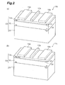
- a hetero-junction transistor will now be described with reference to Part (b) of Fig. 1 , Part (a) of Fig. 2 , and Part (b) of Fig. 2 .
- Fig. 1 Part (b) of Fig. 1 is a drawing schematically illustrating the structure of a group III nitride hetero-junction transistor according to an embodiment.
- the group III nitride hetero-junction transistor (referred to as "transistor” hereafter) 11a includes a first Al X1 In X2 Ga 1-X1-X2 N layer 13a, a second Al Y1 In Y2 Ga 1-Y1-Y2 N layer 15 and electrodes 17a, 18a and 19a.
- the transistor 11a includes the first Al X1 In X2 Ga 1-X1-X2 N layer 13a instead of the first Al X1 In X2 Ga 1-X1-X2 N layer 13.
- the carbon concentration N C 13 in the first Al X1 In X2 Ga 1-X1-X2 N layer 13a is less than 1 ⁇ 10 17 cm -3 .
- the dislocation density D of the second Al Y1 In Y2 Ga 1-Y1-Y2 N layer 15 can be 1 ⁇ 10 8 cm -2 .
- the hetero-junction 21 generates a two-dimensional electron gas layer 25.
- the electrodes 17a, 18a, and 19a correspond to a gate electrode, a source electrode, and a drain electrode, respectively.
- the arrangement of the electrodes 17a, 18a, and 19a is formed on the group III nitride semiconductor epitaxial substrate E2, and the group III nitride semiconductor epitaxial substrate E2 also includes components that correspond to the first Al X1 In X2 Ga 1-X1-X2 N layer 13a, the second Al Y1 In Y2 Ga 1-Y1-Y2 N layer 15, and the substrate 23.
- Carbon atoms in a gallium nitride based semiconductor create levels that capture carriers, so that the gallium nitride based semiconductor with carbon impurity has a reduced leakage current.
- the carbon doping has been used to reduce the leakage current.
- the transistor 11 a and the group III nitride semiconductor epitaxial substrate E2 have a dislocation density of less than 1 ⁇ 10 8 cm -2 in the second Al Y1 In Y2 Ga 1-Y1-Y2 N layer 15, so that leakage current due to the dislocation is sufficiently low.
- the carbon concentration in the first Al X1 In X2 Ga 1-X1-X2 N layer 13a grown thereon is reduced to a level of less than approximately 1 ⁇ 10 17 cm -3 , a increase in the leakage current is made small to be within an acceptable range. Since the carbon concentration N C13 in the first Al X1 In X2 Ga 1-X1-X2 N layer 13a is less than 1 ⁇ 10 17 cm -3 , the number of electron trap levels formed by incorporation of carbon is reduced. Although the application of voltage through the second electrode 18a traps electrons in the trap levels in the Al X1 In X2 Ga 1-X1-X2 N layer 13a near the gate electrode, reducing the carbon concentration makes the number of electron traps small. This reduces the effects of current collapse.
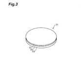
- the substrate 23 has a threading dislocation density Tdd. It is preferred that the dislocation density Tdd be, for example, less than 1 ⁇ 10 8 cm -2 .
- Examples of materials for the substrate 23 encompass GaN, AlN, AlGaN, and InGaN.
- the group III nitride hetero-junction transistor 11b (referred to as "transistor 11b" hereafter) includes a first Al X1 In X2 Ga 1-X1-X2 N layer 13b, a second Al Y1 In Y2 Ga 1-Y1-Y2 N layer 15 and electrodes 17a, 18a and 19a.
- the transistor 11b includes the first Al X1 In X2 Ga 1-X1-X2 N layer 13b instead of the first Al X1 In X2 Ga 1-X1-X2 N layer 13.
- the group III nitride semiconductor epitaxial substrate E3 includes components that correspond to the first Al X1 In X2 Ga 1-X1-X2 N layer 13b, the second Al Y1 In Y2 Ga 1-Y1-Y2 N layer 15 and the substrate 23, and the arrangement of the electrodes 17a, 18a, and 19a is formed on the primary surface of the group III nitride semiconductor epitaxial substrate E3.
- the silicon concentration N Si13 in the first Al X1 In X2 Ga 1-X1-X2 N layer 13b is 1 ⁇ 10 17 cm -3 or higher.
- Silicon in a gallium nitride based semiconductor provides carriers, so that a silicon-doped gallium nitride based semiconductor has a reduced resistivity.
- a gallium nitride based semiconductor has a large dislocation density, carriers provided by silicon therein leads to a large amount of leakage current.
- the group III nitride electronic device 11b and the group III nitride semiconductor epitaxial substrate E3 have a dislocation density D of less than 1 ⁇ 10 8 cm -2 in the second Al Y1 In Y2 Ga 1-Y1-Y2 N layer 15, so that leakage current due to the dislocation is made sufficiently low.
- the leakage current exhibits only a slight increase.
- the relaxation time of the electrons captured in the trap levels is small in the first Al X1 In X2 Ga 1-X1-X2 N layer 13b.
- the trap levels capture electrons in the first Al X1 In X2 Ga 1-X1-X2 N layer 13b near the gate electrode in response to the application of voltage through the first and second electrodes 17a and 19a
- the trapped electrons are released within a short period of time after the applied voltage has been removed because the silicon concentration in the first Al X1 In X2 Ga 1-X1-X2 N layer 13b is 1 ⁇ 10 17 cm -3 or higher. Therefore, the effects of current collapse are moderated.
- the silicon concentration N Si13 is preferably 1 ⁇ 10 19 cm -3 or less.
- Part (b) of Fig. 2 is a schematic view illustrating the structure of a group III nitride hetero-junction transistor according to an embodiment.
- the group III nitride hetero-junction transistor 11c (referred to as "transistor 11c" hereafter) includes a first Al X1 In X2 Ga 1-X1-X2 N layer 13c, a second Al Y1 In Y2 Ga 1-Y1-Y2 N layer 15 and electrodes 17a, 18a and 19a.
- the transistor 11c includes the first Al X1 In X2 Ga 1-X1-X2 N layer 13c instead of the first Al X1 In X2 Ga 1-X1-X2 N layer 13.
- the group III nitride semiconductor epitaxial substrate E4 includes components that correspond to the first Al X1 In X2 Ga 1-X1-X2 N layer 13c, the second Al Y1 In Y2 Ga 1-Y1-Y2 N layer 15, and the substrate 23.
- the arrangement of the electrodes 17a, 18a, and 19a is formed on the primary surface of the group III nitride semiconductor epitaxial substrate E4.
- carbon in a gallium nitride based semiconductor works as traps that carriers capture
- silicon in a gallium nitride based semiconductor works as donors that provide carriers.
- Carbon is incorporated in a gallium nitride based semiconductor, and trap levels formed by the incorporated carbon can capture carriers, leading to worsening current collapse.
- the gallium nitride based semiconductor is doped with silicon at a concentration higher than that of carbon, so that the number of carriers is greater than the number of trap levels, leading to a reduced resistivity. Therefore, after the applied voltage is removed, the trapped electrons are released in a short period of time. This moderates the effects of current collapse.
- the transistor 11c and the group III nitride semiconductor epitaxial substrate E4 have a dislocation density of less than 1 ⁇ 10 8 cm -2 in the second Al Y1 In Y2 Ga 1-Y1-Y2 N layer 15, so that leakage current due to the dislocation is sufficiently low. Accordingly, in the first Al X1 In X2 Ga 1-X1-X2 N layer 13c having the silicon concentration higher than its carbon concentration, increase in the leakage current is made slight.
- AlGaN layers were grown under various growth pressures as in the experiments described above.
- Epitaxial wafers A-2 through E-2 were fabricated under a growth pressure of 75 torr.
- Epitaxial wafers A-3 through E-3 were fabricated under a growth pressure of 100 torr.
- Epitaxial wafers A-4 through E-4 were fabricated under a growth pressure of 150 torr.
- Epitaxial wafers A-5 through E-5 were fabricated under a growth pressure of 200 torr.
- electrodes were formed on each epitaxial substrate to fabricate a transistor of a HEMT structure.
- the gate electrode had a ring shape with a gate width Wg of 0.5 mm and a drain-gate distance Lgd of 10 ⁇ m, and the drain electrode is located inside the ring whereas the source electrode is located outside the ring to surround it.
- the first measurement of on-resistance was carried out before applying a reverse bias and the second measurement of on-resistance was carried out after a voltage Vds of 100 V had been applied for 5 minutes.
- the current collapse was defined as the ratio of the above two on-resistance values (on-resistance after biasing/on-resistance before biasing). If the current collapse does not occur, this on-resistance ratio is equal to one. If the current collapse occurs, the on-resistance ratio is greater than one.
- the leakage current is defmed by Igs (current between the gate and the source) measured at an applied voltage Vds of 100 V.
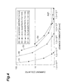
- Fig. 4 shows the experimental results.
- Fig. 4 indicates characteristic curves: C1, C2, C3, and C4.
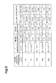
- Fig. 5 summarizes the experimental results shown in Fig. 4 .
- Fig. 5 shows the carbon concentration of AlGaNs grown on the GaN substrate.
- the carbon concentration of AlGaN on the Sap substrate is 3.2 ⁇ 10 18 cm -3 ;
- the leakage current is 2.2 ⁇ 10 -9 A/mm; and the current collapse is 10.41.
- the term "Sap substrate” stands for sapphire substrate.
- the trade-off relationship between the leakage current and the current collapse holds regardless of the type of the substrate.
- the carbon concentration is, for example, 9.7 ⁇ 10 16 cm -3 , which is less than 1.0 ⁇ 10 17 cm -3 .
- the HEMT structure on the GaN substrate with low dislocation density has excellent characteristics of both the leakage current and the current collapse.
- the leakage current of the epitaxial substrate prepared with the sapphire substrate and the SiC substrate used in the experiment is greater than that of the epitaxial substrate prepared with the GaN substrate, and the current collapse also increases as the carbon concentration increases.
- the leakage current of the epitaxial substrate prepared with the GaN substrate in the experiment is small. Even when the carbon concentration is reduced to suppress current collapse, the increase in leakage current is within an acceptable range. In other words, this reveals that an epitaxial substrate using a GaN substrate with low dislocation density can partially improve the trade-off relationship.
- a GaN substrate with low dislocation density is suitable for growing a buffer layer with low dislocation density.
- This buffer layer is used as an underlying layer of low dislocation density for growing the AlGaN barrier layer thereon.
- an AlN substrate or an AlN/sapphire template that have a low dislocation density can also weaken the trade-off relationship (the trade-off relationship between leakage current and current collapse) if its dislocation density is 1 ⁇ 10 8 cm -2 or less.
- the leakage current slightly increases as the carbon concentration is reduced by use of an increased growth pressure.
- Such an increase in the leakage current is sufficiently small, which is acceptable, and the growth recipes can reduce the current collapse to a practical level.
- the practical level of current collapse is marked by "Ref1" in Fig. 4 .
- the level “Ref1” is, for example, approximately 1.3 in terms of on-resistance ratio.
- Fig. 6 is a graph showing the relationship between the carbon concentration and the current collapse.
- Fig. 6 shows characteristic curves I1 to I4.
- a device exhibiting large current collapse has a large increase in the on-resistance. Accordingly, it is preferred that the current collapse be approximately 1.3 or less.
- the value of "Ref2" in Fig. 6 indicates 1.3.
- the dislocation density range from 2 ⁇ 10 9 cm -3 to 5 ⁇ 10 6 cm -3 permits a practical level of current collapse.
- Fig. 7 is a graph indicating the relationship between the dislocation density and the leakage current density.
- Fig. 7 shows characteristic curves, J1 to J5.
- a practical level of leakage current is 1 ⁇ 10 -7 A/cm 2 or less. In Fig. 7 , this value is referred to as "Ref3."
- the leakage current decreases as the carbon concentration decreases. But, taking the value of the current collapse into consideration, the carbon concentration is preferably less than 1 ⁇ 10 17 cm -3 . When the carbon concentration is less than 1 ⁇ 10 17 cm -3 and the dislocation density is less than 1 ⁇ 10 8 cm -2 , the leakage current and the current collapse both fall in the practical ranges.
- the growth pressure was varied to modify the carbon concentration.
- the carbon concentration can be reduced by modifying other parameters, such as growth temperature, flow rate of ammonia, V/III molar ratio, and deposition rate. According to experiments conducted by the inventors, varying these parameters produced similar results.
- An increase in the growth temperature reduces the carbon concentration.
- An increase in the flow rate of ammonia reduces the carbon concentration.
- An increase in the V/III ratio reduces the carbon concentration.
- a decrease in the growth rate reduces the carbon concentration.
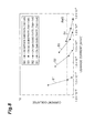
- Epitaxial substrates were fabricated with various silicon concentrations.
- the fabrication conditions used were the same as those for the epitaxial substrates A-3, B-3, C-3, and D-3 (under a growth pressure of 100 torr for AlGaNs), and AlGaN layers for the present epitaxial substrates were doped with silicon at 3.1 ⁇ 10 6 cm -3 , 1.1 ⁇ 10 17 cm -3 , or 3.7 ⁇ 10 17 cm -3 .
- the index of current collapse and the leakage current were evaluated in these epitaxial substrates.
- Fig. 8 shows the experimental results.
- Fig. 8 indicates characteristic curves, S1, S2, S3, and S4.
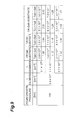
- Fig. 9 summarizes the results shown in Fig. 8 .
- Fig. 9 shows a table of the silicon concentrations of AlGaNs over the GaN substrates.
- the carbon concentration in AlGaN over the Sap substrate is 3.4 ⁇ 10 17 cm -3 ;
- the silicon concentration is 3.1 ⁇ 10 16 cm -3 ;
- the leakage current is 3.9 ⁇ 10 -6 A/mm; and the index of current collapse is 1.36.
- the carbon concentration was set to 3.4 ⁇ 10 17 cm -3 regardless of the silicon concentration.
- the silicon concentration is, for example, 1.1 ⁇ 10 17 cm -3 , which is not smaller than 1.0 ⁇ 10 17 cm -3 .
- the silicon concentration is, for example, 1.1 ⁇ 10 17 cm -3 , which is not smaller than 1.0 ⁇ 10 17 cm -3 .
- a silicon concentration equal to or higher than the carbon concentration can provide satisfactory characteristics of both the leakage current and the current collapse in the HEMT structure on the GaN substrate with low dislocation density.
- AlGaN with high dislocation density such as in AlGaN grown over the sapphire substrate or the SiC substrate
- doping AlGaN with silicon significantly increases the leakage current but decreases the current collapse.
- AlGaN with low dislocation density such as in AlGaN grown on the GaN substrate with low dislocation density
- the increase in the leakage current by addition of Si is sufficiently low while the current collapse can be significantly reduced.
- their suitable concentration ranges are as follows.
- the carbon concentration is preferably 3 ⁇ 10 16 cm -3 or higher because it is difficult to reduce carbon to a concentration lower than the above value.
- the carbon concentration is preferably 1 ⁇ 10 19 cm -3 or less because otherwise a satisfactory epitaxial film cannot be obtained.
- the silicon concentration is preferably 3 ⁇ 10 16 cm -3 or higher because it is difficult to reduce the carbon concentration to 3 ⁇ 10 16 cm -3 or less.
- the silicon concentration is preferably 1 ⁇ 10 19 cm -3 or less because the leakage current increases if the silicon concentration is too high.
- a reduction in the carbon concentration in the buffer layer can produce the same effects as those according to this embodiment. Specifically, it is effective in reducing the current collapse.
- the present invention is not limited to the embodiments described in the embodiments. It also achieves equivalent effects in lateral electronic devices such as a lateral Schottky barrier diode.
- reducing the carbon concentration to less than 1 ⁇ 10 17 cm -3 in AlGaN can simultaneously improve the current collapse and the leakage current.
- Increasing the silicon concentration to 1 ⁇ 10 17 cm -3 or higher in AlGaN can also simultaneously improve the current collapse and the leakage current.
- using a silicon concentration greater than the carbon concentration in AlGaN can simultaneously improve the current collapse and the leakage current.
- an underlying semiconductor region with low dislocation density makes it possible to use deposition recipes that increase the leakage current. This partially breaks through the trade-off relationship between the leakage current and the current collapse, and can mostly suppress the current collapse while achieving low leakage current.
Landscapes
- Junction Field-Effect Transistors (AREA)
- Electrodes Of Semiconductors (AREA)
Applications Claiming Priority (2)
| Application Number | Priority Date | Filing Date | Title |
|---|---|---|---|
| JP2007286534A JP4462330B2 (ja) | 2007-11-02 | 2007-11-02 | Iii族窒化物電子デバイス |
| PCT/JP2008/069564 WO2009057601A1 (fr) | 2007-11-02 | 2008-10-28 | Dispositif électronique à nitrure iii et substrat épitaxial semi-conducteur à nitrure iii |
Publications (2)
| Publication Number | Publication Date |
|---|---|
| EP2211376A1 true EP2211376A1 (fr) | 2010-07-28 |
| EP2211376A4 EP2211376A4 (fr) | 2012-04-04 |
Family
ID=40590991
Family Applications (1)
| Application Number | Title | Priority Date | Filing Date |
|---|---|---|---|
| EP08845789A Withdrawn EP2211376A4 (fr) | 2007-11-02 | 2008-10-28 | Dispositif électronique à nitrure iii et substrat épitaxial semi-conducteur à nitrure iii |
Country Status (7)
| Country | Link |
|---|---|
| US (1) | US8541816B2 (fr) |
| EP (1) | EP2211376A4 (fr) |
| JP (1) | JP4462330B2 (fr) |
| KR (1) | KR20100074187A (fr) |
| CN (1) | CN101842884B (fr) |
| TW (1) | TW200937634A (fr) |
| WO (1) | WO2009057601A1 (fr) |
Families Citing this family (17)
| Publication number | Priority date | Publication date | Assignee | Title |
|---|---|---|---|---|
| JP4462330B2 (ja) | 2007-11-02 | 2010-05-12 | 住友電気工業株式会社 | Iii族窒化物電子デバイス |
| JP2011035066A (ja) * | 2009-07-30 | 2011-02-17 | Sumitomo Electric Ind Ltd | 窒化物半導体素子、及び窒化物半導体素子を作製する方法 |
| JP2010045416A (ja) * | 2009-11-25 | 2010-02-25 | Sumitomo Electric Ind Ltd | Iii族窒化物電子デバイス |
| JP2012033575A (ja) * | 2010-07-28 | 2012-02-16 | Sumitomo Electric Ind Ltd | 半導体装置 |
| JP2013033930A (ja) * | 2011-06-29 | 2013-02-14 | Sumitomo Electric Ind Ltd | Iii族窒化物半導体素子、及び、iii族窒化物半導体素子の製造方法 |
| JP6015053B2 (ja) * | 2012-03-26 | 2016-10-26 | 富士通株式会社 | 半導体装置の製造方法及び窒化物半導体結晶の製造方法 |
| JP5656930B2 (ja) * | 2012-07-05 | 2015-01-21 | 古河電気工業株式会社 | 窒化物系化合物半導体素子 |
| CN103828030B (zh) * | 2012-08-10 | 2017-11-10 | 日本碍子株式会社 | 半导体元件、hemt元件、以及半导体元件的制造方法 |
| EP2888390A1 (fr) | 2012-08-24 | 2015-07-01 | Sixpoint Materials Inc. | Tranche de semi-isolant à base de nitrure du groupe iii dopé au bismuth et son procédé de production |
| JP5787417B2 (ja) * | 2013-05-14 | 2015-09-30 | コバレントマテリアル株式会社 | 窒化物半導体基板 |
| JP6175009B2 (ja) * | 2014-02-06 | 2017-08-02 | 住友化学株式会社 | 高耐圧窒化ガリウム系半導体デバイス及びその製造方法 |
| JP2015176936A (ja) * | 2014-03-13 | 2015-10-05 | 株式会社東芝 | 半導体装置 |
| JP6305137B2 (ja) * | 2014-03-18 | 2018-04-04 | 住友化学株式会社 | 窒化物半導体積層物および半導体装置 |
| JP6249868B2 (ja) * | 2014-04-18 | 2017-12-20 | サンケン電気株式会社 | 半導体基板及び半導体素子 |
| US9419125B1 (en) | 2015-06-16 | 2016-08-16 | Raytheon Company | Doped barrier layers in epitaxial group III nitrides |
| JP6682391B2 (ja) | 2016-07-22 | 2020-04-15 | 株式会社東芝 | 半導体装置、電源回路、及び、コンピュータ |
| CN117542887B (zh) * | 2024-01-10 | 2024-04-30 | 英诺赛科(珠海)科技有限公司 | 一种氮化镓射频器件以及制备方法 |
Family Cites Families (17)
| Publication number | Priority date | Publication date | Assignee | Title |
|---|---|---|---|---|
| JP2001015437A (ja) | 1999-06-29 | 2001-01-19 | Nec Corp | Iii族窒化物結晶成長法 |
| US6787814B2 (en) * | 2000-06-22 | 2004-09-07 | Showa Denko Kabushiki Kaisha | Group-III nitride semiconductor light-emitting device and production method thereof |
| JP4554803B2 (ja) | 2000-12-04 | 2010-09-29 | 独立行政法人理化学研究所 | 低転位バッファーおよびその製造方法ならびに低転位バッファーを備えた素子 |
| JP3569807B2 (ja) | 2002-01-21 | 2004-09-29 | 松下電器産業株式会社 | 窒化物半導体素子の製造方法 |
| JP2003282929A (ja) | 2002-03-22 | 2003-10-03 | Osaka Gas Co Ltd | 受光素子の作製方法 |
| JP4179539B2 (ja) * | 2003-01-15 | 2008-11-12 | 富士通株式会社 | 化合物半導体装置及びその製造方法 |
| JP2006114655A (ja) * | 2004-10-14 | 2006-04-27 | Hitachi Cable Ltd | 半導体エピタキシャルウェハ及び電界効果トランジスタ |
| US7456443B2 (en) * | 2004-11-23 | 2008-11-25 | Cree, Inc. | Transistors having buried n-type and p-type regions beneath the source region |
| JP2006295126A (ja) | 2005-03-15 | 2006-10-26 | Sumitomo Electric Ind Ltd | Iii族窒化物半導体素子およびエピタキシャル基板 |
| JP2006261474A (ja) | 2005-03-18 | 2006-09-28 | Furukawa Electric Co Ltd:The | 窒化物系半導体デバイス |
| JP4895520B2 (ja) | 2005-03-28 | 2012-03-14 | 日本電信電話株式会社 | ショットキーダイオードおよびその製造方法 |
| JP4792814B2 (ja) | 2005-05-26 | 2011-10-12 | 住友電気工業株式会社 | 高電子移動度トランジスタ、電界効果トランジスタ、エピタキシャル基板、エピタキシャル基板を作製する方法およびiii族窒化物系トランジスタを作製する方法 |
| WO2007007589A1 (fr) | 2005-07-08 | 2007-01-18 | Nec Corporation | Transistor à effet de champ et son procédé de fabrication |
| JP2007027276A (ja) | 2005-07-13 | 2007-02-01 | Oki Electric Ind Co Ltd | 半導体素子の製造方法及び半導体素子 |
| US20070018198A1 (en) | 2005-07-20 | 2007-01-25 | Brandes George R | High electron mobility electronic device structures comprising native substrates and methods for making the same |
| WO2007013257A1 (fr) | 2005-07-29 | 2007-02-01 | Matsushita Electric Industrial Co., Ltd. | Dispositif semi-conducteur au nitrure |
| JP4462330B2 (ja) | 2007-11-02 | 2010-05-12 | 住友電気工業株式会社 | Iii族窒化物電子デバイス |
-
2007
- 2007-11-02 JP JP2007286534A patent/JP4462330B2/ja not_active Expired - Fee Related
-
2008
- 2008-10-28 WO PCT/JP2008/069564 patent/WO2009057601A1/fr not_active Ceased
- 2008-10-28 EP EP08845789A patent/EP2211376A4/fr not_active Withdrawn
- 2008-10-28 CN CN2008801142642A patent/CN101842884B/zh not_active Expired - Fee Related
- 2008-10-28 KR KR1020107008135A patent/KR20100074187A/ko not_active Withdrawn
- 2008-10-28 US US12/740,770 patent/US8541816B2/en not_active Expired - Fee Related
- 2008-10-31 TW TW097142286A patent/TW200937634A/zh unknown
Also Published As
| Publication number | Publication date |
|---|---|
| US8541816B2 (en) | 2013-09-24 |
| JP4462330B2 (ja) | 2010-05-12 |
| US20100230687A1 (en) | 2010-09-16 |
| EP2211376A4 (fr) | 2012-04-04 |
| KR20100074187A (ko) | 2010-07-01 |
| TW200937634A (en) | 2009-09-01 |
| JP2009117482A (ja) | 2009-05-28 |
| WO2009057601A1 (fr) | 2009-05-07 |
| CN101842884A (zh) | 2010-09-22 |
| CN101842884B (zh) | 2012-05-16 |
Similar Documents
| Publication | Publication Date | Title |
|---|---|---|
| US8541816B2 (en) | III nitride electronic device and III nitride semiconductor epitaxial substrate | |
| Saitoh et al. | Extremely low on-resistance and high breakdown voltage observed in vertical GaN Schottky barrier diodes with high-mobility drift layers on low-dislocation-density GaN substrates | |
| US8653561B2 (en) | III-nitride semiconductor electronic device, and method of fabricating III-nitride semiconductor electronic device | |
| US8969920B2 (en) | Vertical GaN-based semiconductor device | |
| TWI663635B (zh) | 使用離子植入之使高電阻率氮化物緩衝層的半導體材料生長 | |
| US8134181B2 (en) | Semiconductor device | |
| CN113380623A (zh) | 通过p型钝化实现增强型HEMT的方法 | |
| TW202109890A (zh) | 具有高耐壓能力的高電子遷移率電晶體及其製備方法 | |
| US20220157980A1 (en) | Nitride semiconductor device | |
| US10777654B2 (en) | Method for manufacturing nitrogen-face polarity gallium nitride epitaxial structure | |
| US20110254055A1 (en) | Field effect transistor and manufacturing method thereof | |
| US7750351B2 (en) | Epitaxial substrate for field effect transistor | |
| Zhao et al. | AlGaN/GaN HEMTs with a magnetron-sputtered AlN buffer layer | |
| CN210272373U (zh) | 一种具有高耐压能力的高电子迁移率晶体管 | |
| TWI572036B (zh) | Nitride crystal structure | |
| US9331169B2 (en) | Nitride semiconductor Schottky diode and method for manufacturing same | |
| Ahmad et al. | GaN: Be I-layer-based high-power pin diodes achieving large quasi-vertical MBE breakdown performance | |
| US12100759B2 (en) | Semiconductor device, manufacturing method and electronic equipment | |
| CN113838935B (zh) | 一种半导体器件、制造方法及其应用 | |
| JP2010045416A (ja) | Iii族窒化物電子デバイス | |
| WO2012140915A1 (fr) | Dispositif semi-conducteur | |
| KR20230032751A (ko) | 반도체 소자 및 이의 제조방법 | |
| CN119545836B (zh) | 一种氮化镓器件结构及其制备方法 | |
| Tang et al. | Growth and characterization of InGaN back barrier HEMTs structure with a compositionally step-graded AlGaN layer | |
| Ni et al. | Breakdown Mechanism of AlGaN/GaN-based HFET With Carbon-doped GaN Buffer Layer grown on Si substrate |
Legal Events
| Date | Code | Title | Description |
|---|---|---|---|
| PUAI | Public reference made under article 153(3) epc to a published international application that has entered the european phase |
Free format text: ORIGINAL CODE: 0009012 |
|
| 17P | Request for examination filed |
Effective date: 20100521 |
|
| AK | Designated contracting states |
Kind code of ref document: A1 Designated state(s): AT BE BG CH CY CZ DE DK EE ES FI FR GB GR HR HU IE IS IT LI LT LU LV MC MT NL NO PL PT RO SE SI SK TR |
|
| AX | Request for extension of the european patent |
Extension state: AL BA MK RS |
|
| DAX | Request for extension of the european patent (deleted) | ||
| A4 | Supplementary search report drawn up and despatched |
Effective date: 20120305 |
|
| RIC1 | Information provided on ipc code assigned before grant |
Ipc: H01L 29/205 20060101ALI20120228BHEP Ipc: H01L 29/207 20060101ALI20120228BHEP Ipc: H01L 29/872 20060101ALI20120228BHEP Ipc: H01L 29/778 20060101AFI20120228BHEP |
|
| 17Q | First examination report despatched |
Effective date: 20130403 |
|
| STAA | Information on the status of an ep patent application or granted ep patent |
Free format text: STATUS: THE APPLICATION IS DEEMED TO BE WITHDRAWN |
|
| 18D | Application deemed to be withdrawn |
Effective date: 20130814 |